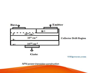
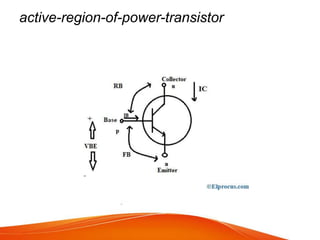
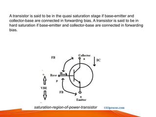
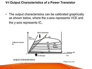
What is a Power
Transistor?
The three-terminal device which is designed
specifically to control high current – voltage
rating and handle a large number of power
levels in a device or a circuit is a power
transistor.
The classification of power
transistor include the following.
1. Bipolar junction transistor (BJTs)
2. Metal oxide semiconductor field-effect
transistor (MOSFETs)
3. Static induction transistor (SITs)
4. Insulated-gate bipolar transistor (IGBTs).
Bipolar Junction Transistor
A BJT is a bipolar junction transistor, which is capable of
handling two polarities (holes and electrons), it can be used as a
switch or as an amplifier and also known as a current control
device. The following are the characteristics of a Power BJT,
they are
• It has a larger size, so that maximum current can flow through
it
• The breakdown voltage is high
• It has higher current carrying and high-power handling
capability
• It has a higher on-state voltage drop
• High power application.
•
Structure of Power Transistor
The Power Transistor BJT is a vertically oriented device having a large
area of cross-sectional with alternate P and N-type layers are
connected together. It can be designed using P-N-P or an N-P-
N transistor.
pnp-and-npn-transistor
• The following construction shows a P-N-P type,
which consists of three terminals emitter, base,
and collector. Where the emitter terminal is
connected to highly doped n-type layer, below
which a moderately doped p-layer of 1016 cm-3
concentration is present, and a lightly doped n-
layer of 1014 cm-3 concentration, which is also
named as collector drift region, where the
collector drift region decides the break-over
voltage of the device and at the bottom, it has an
n+ layer which is highly doped n-type layer of
1019 cm-3 concentration, where the collector is
etched away for user interface
NPN-power-transistor-construction
Operation of Power Transistor
Power Transistor BJT works in four regions of
operation they are
• Cut off region
• Active region
• Quasi saturation region
• Hard saturation region.
A power transistor is said to be in a cut off
mode if the n-p-n power transistor is connected
in reverse bias where
case(i): The base terminal of the transistor is connected to negative and emitter terminals of
the transistor is connected to positive, and
case(ii): The collector terminal of the transistor is connected to the negative and base
terminal of the transistor is connected to positive that is base-emitter and collector-emitter is in
reverse bias
cutoff-region-of-power-transistor
• Hence there will be no flow of output current to the base
of the transistor where IBE = 0, and also there will be no
output current flowing through the collector to emitter
since IC = IB = 0 which indicates transistor is in off state
that is a cut off region. But a small fraction of leakage
current flows throw the transistor from collector to emitter
i.e, ICEO.
• A transistor is said to be inactive state only when the
base-emitter region is forward bias and collector-base
region reverse bias. Hence there will be a flow of current
IB in the base of transistor and flow of current IC through
the collector to emitter of the transistor. When IB
increases IC also increases.
active-region-of-power-transistor
A transistor is said to be in the quasi saturation stage if base-emitter and
collector-base are connected in forwarding bias. A transistor is said to be in
hard saturation if base-emitter and collector-base are connected in forwarding
bias.
saturation-region-of-power-transistor
V-I Output Characteristics of a Power Transistor
• The output characteristics can be calibrated graphically
as shown below, where the x-axis represents VCE and
the y-axis represents IC.
output-characteristics
• The below graph represents various regions like the
cut-off region, active region, hard saturation region,
quasi saturation region.
• For different values of VBE, there are different current
values IB0, IB1, IB2, IB3, IB4, IB5, IB6.
• Whenever there is no current flow, it means the
transistor is off. But few current flows which are ICEO.
• .
• For increased value of IB = 0, 1,2, 3, 4, 5. Where
IB0 is the minimum value and IB6 is the
maximum value. When VCE increases ICE also
increases slightly. Where IC = ßIB, hence the
device is known as a current control device.
Which means the device is in active region,
which exists for a particular period.
• Once the IC has reached to maximum the
transistor switches to the saturation region
• Where it has two saturation regions quasi
saturation region and hard saturation region.
• A transistor is said to be in a quasi saturation
region if and only if the switching speed from on
to off or off to on is fast. This type of saturation is
observed in the medium-frequency application.
• Whereas in a hard saturation region the
transistor requires a certain amount of time to
switch from on to off or off to on state. This type
of saturation is observed in the low-frequency
applications.
• Advantages
• The advantages of power BJT are,
• Voltage gain is high
• The density of the current is high
• The forward voltage is low
• The gain of bandwidth is large.
Disadvantages
• The disadvantages of power BJT are,
• Thermal stability is low
• It is noisier
• Controlling is a bit complex.
• Applications
• The applications of power BJT are,
• Switch-mode power supplies (SMPS)
• Relays
• Power amplifiers
• DC to AC converters
• Power control circuits.
FAQs
1). Difference between transistor and power transistor?
• A transistor is a three or four-terminal electronic device,
where on applying an input current to a pair of the
terminals of the transistor, one can observe a change in
current in another terminal of that transistor. A transistor
acts like a switch or an amplifier. Whereas a power
transistor acts like a heat sink, which protects the circuit
from damage. It is larger in size than a normal transistor.
2). Which region of transistor makes it switch faster
from on to off or off to on?
• The power transistor when it is in quasi saturation
switches faster from on to off or off to on.
3) What does N in NPN or PNP transistor mean?
• N in NPN and PNP type transistor represents the
type of charge carriers used, which is in an N-type
the majority charge carriers are electrons. Hence in
NPN two N-type charge carriers are sandwiched
with a P-type, and in PNP single N-type charge
carrier is sandwiched between two P-type charge
carriers.
4) What is the unit of the transistor?
• The standard units of a transistor for electrical
measurement are Ampere (A), Volt (V), and Ohm
(Ω) respectively.
5) Does transistor work on ac or dc?
• A transistor is a variable resistor that can work on
both AC and DC but cannot convert from AC to DC
or DC to AC.
• The transistor a basic component of a digital
system, they are of two types based on their
structure and based on their functionality.
• The transistor which is used for controlling large
voltage and current is a power BJT (bipolar
transistor) is a power transistor.
• It is also known as a voltage-current control device
that operates in 4 regions cut-off, active, quasi
saturation, and hard saturation based on the
supplies given to the transistor.
• The main advantage of a power transistor is it acts
as a current control device.

What is a Power Transistor.pptx

  • 1.
    What is aPower Transistor? The three-terminal device which is designed specifically to control high current – voltage rating and handle a large number of power levels in a device or a circuit is a power transistor. The classification of power transistor include the following. 1. Bipolar junction transistor (BJTs) 2. Metal oxide semiconductor field-effect transistor (MOSFETs) 3. Static induction transistor (SITs) 4. Insulated-gate bipolar transistor (IGBTs).
  • 2.
    Bipolar Junction Transistor ABJT is a bipolar junction transistor, which is capable of handling two polarities (holes and electrons), it can be used as a switch or as an amplifier and also known as a current control device. The following are the characteristics of a Power BJT, they are • It has a larger size, so that maximum current can flow through it • The breakdown voltage is high • It has higher current carrying and high-power handling capability • It has a higher on-state voltage drop • High power application. •
  • 3.
    Structure of PowerTransistor The Power Transistor BJT is a vertically oriented device having a large area of cross-sectional with alternate P and N-type layers are connected together. It can be designed using P-N-P or an N-P- N transistor. pnp-and-npn-transistor
  • 4.
    • The followingconstruction shows a P-N-P type, which consists of three terminals emitter, base, and collector. Where the emitter terminal is connected to highly doped n-type layer, below which a moderately doped p-layer of 1016 cm-3 concentration is present, and a lightly doped n- layer of 1014 cm-3 concentration, which is also named as collector drift region, where the collector drift region decides the break-over voltage of the device and at the bottom, it has an n+ layer which is highly doped n-type layer of 1019 cm-3 concentration, where the collector is etched away for user interface
  • 5.
  • 6.
    Operation of PowerTransistor Power Transistor BJT works in four regions of operation they are • Cut off region • Active region • Quasi saturation region • Hard saturation region. A power transistor is said to be in a cut off mode if the n-p-n power transistor is connected in reverse bias where
  • 7.
    case(i): The baseterminal of the transistor is connected to negative and emitter terminals of the transistor is connected to positive, and case(ii): The collector terminal of the transistor is connected to the negative and base terminal of the transistor is connected to positive that is base-emitter and collector-emitter is in reverse bias cutoff-region-of-power-transistor
  • 8.
    • Hence therewill be no flow of output current to the base of the transistor where IBE = 0, and also there will be no output current flowing through the collector to emitter since IC = IB = 0 which indicates transistor is in off state that is a cut off region. But a small fraction of leakage current flows throw the transistor from collector to emitter i.e, ICEO. • A transistor is said to be inactive state only when the base-emitter region is forward bias and collector-base region reverse bias. Hence there will be a flow of current IB in the base of transistor and flow of current IC through the collector to emitter of the transistor. When IB increases IC also increases.
  • 9.
  • 10.
    A transistor issaid to be in the quasi saturation stage if base-emitter and collector-base are connected in forwarding bias. A transistor is said to be in hard saturation if base-emitter and collector-base are connected in forwarding bias. saturation-region-of-power-transistor
  • 11.
    V-I Output Characteristicsof a Power Transistor • The output characteristics can be calibrated graphically as shown below, where the x-axis represents VCE and the y-axis represents IC. output-characteristics
  • 12.
    • The belowgraph represents various regions like the cut-off region, active region, hard saturation region, quasi saturation region. • For different values of VBE, there are different current values IB0, IB1, IB2, IB3, IB4, IB5, IB6. • Whenever there is no current flow, it means the transistor is off. But few current flows which are ICEO. • .
  • 13.
    • For increasedvalue of IB = 0, 1,2, 3, 4, 5. Where IB0 is the minimum value and IB6 is the maximum value. When VCE increases ICE also increases slightly. Where IC = ßIB, hence the device is known as a current control device. Which means the device is in active region, which exists for a particular period. • Once the IC has reached to maximum the transistor switches to the saturation region
  • 14.
    • Where ithas two saturation regions quasi saturation region and hard saturation region. • A transistor is said to be in a quasi saturation region if and only if the switching speed from on to off or off to on is fast. This type of saturation is observed in the medium-frequency application. • Whereas in a hard saturation region the transistor requires a certain amount of time to switch from on to off or off to on state. This type of saturation is observed in the low-frequency applications.
  • 15.
    • Advantages • Theadvantages of power BJT are, • Voltage gain is high • The density of the current is high • The forward voltage is low • The gain of bandwidth is large. Disadvantages • The disadvantages of power BJT are, • Thermal stability is low • It is noisier • Controlling is a bit complex. • Applications • The applications of power BJT are, • Switch-mode power supplies (SMPS) • Relays • Power amplifiers • DC to AC converters • Power control circuits.
  • 16.
    FAQs 1). Difference betweentransistor and power transistor? • A transistor is a three or four-terminal electronic device, where on applying an input current to a pair of the terminals of the transistor, one can observe a change in current in another terminal of that transistor. A transistor acts like a switch or an amplifier. Whereas a power transistor acts like a heat sink, which protects the circuit from damage. It is larger in size than a normal transistor. 2). Which region of transistor makes it switch faster from on to off or off to on? • The power transistor when it is in quasi saturation switches faster from on to off or off to on.
  • 17.
    3) What doesN in NPN or PNP transistor mean? • N in NPN and PNP type transistor represents the type of charge carriers used, which is in an N-type the majority charge carriers are electrons. Hence in NPN two N-type charge carriers are sandwiched with a P-type, and in PNP single N-type charge carrier is sandwiched between two P-type charge carriers. 4) What is the unit of the transistor? • The standard units of a transistor for electrical measurement are Ampere (A), Volt (V), and Ohm (Ω) respectively. 5) Does transistor work on ac or dc? • A transistor is a variable resistor that can work on both AC and DC but cannot convert from AC to DC or DC to AC.
  • 18.
    • The transistora basic component of a digital system, they are of two types based on their structure and based on their functionality. • The transistor which is used for controlling large voltage and current is a power BJT (bipolar transistor) is a power transistor. • It is also known as a voltage-current control device that operates in 4 regions cut-off, active, quasi saturation, and hard saturation based on the supplies given to the transistor. • The main advantage of a power transistor is it acts as a current control device.