Downloaded 106 times

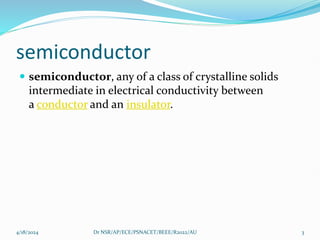
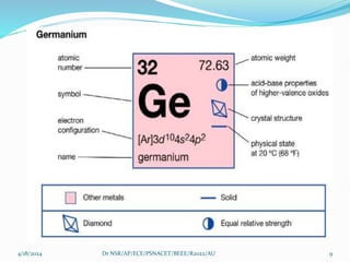
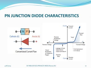
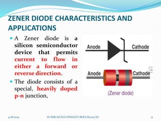


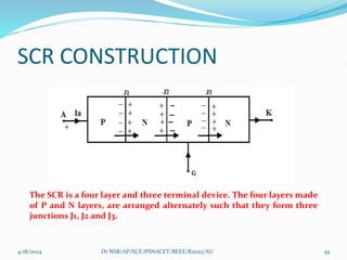
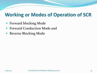
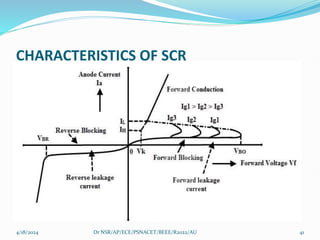

The document provides an overview of semiconductor materials, specifically comparing conductors, semiconductors, and insulators based on their electrical properties and applications. It describes various semiconductor devices such as PN junction diodes, Zener diodes, bipolar junction transistors (BJTs), junction field effect transistors (JFETs), silicon-controlled rectifiers (SCRs), and metal-oxide-semiconductor field-effect transistors (MOSFETs), detailing their structure, operation, and uses in electronics. Additionally, it covers the importance of biasing in transistors and the characteristics of each type of semiconductor device.


