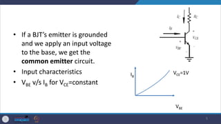
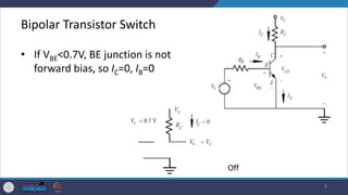
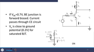
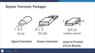
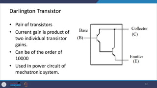
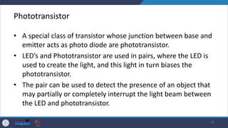
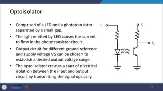
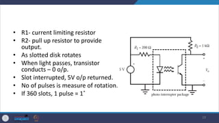
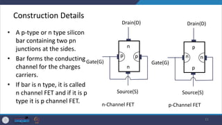
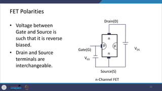
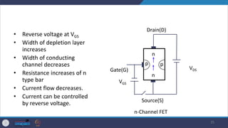
MECHATRONICS
APPLICATION OF TRANSISTORS
PUSHPARAJ MANI PATHAK
MECHANICAL & INDUSTRIAL ENGINEEING, IIT ROORKEE
1
Introduction
• Because of the Bipolar Junction Transistor (BJT) base-collector
current characteristics, it can be used to
– amplify current
– simply switch current on and off.
• Transistor as a switch is basis for most digital computers
because it allows easy implementation of a two state binary
representation.
• We focus on switch design in our mechatronic applications
2
Transistor Connections
• Common base connection
• Common emitter connection
• Common collector connection
3
Common Emitter Connection
• Input current IB
• Output current IC
• Base current amplification
factor =
∆𝐼𝐶
∆𝐼𝐵
= 𝛽
• ∆𝐼𝐵 < 5% ∆𝐼𝐸
• 𝛽 > 20 (IC ≈ IE)
• 𝛽 ≈ 100
4
• If a BJT’s emitter is grounded
and we apply an input voltage
to the base, we get the
common emitter circuit.
• Input characteristics
• VBE v/s IB for VCE=constant
5
VBE
IB
VCE=1V
Output Characteristic
• VCE v/s IC for constant base
current (IB)
• As IB increases, base to emitter
conducts when VBE = 0.6V,
IC= 𝛽IB
• As IB is further increased, VBE
slowly increases to 0.7V, IC
rises exponentially.
6
• As IC increases, voltage
drop across RC increases,
so VCE drops towards
ground.
• Transistor is said to go to
saturation i.e., collector
current is determined by
RC and linear relation
between IC and IB no
longer holds.
7
• When designing a transistor switch, we need to guarantee
that the transistor is in fully saturation condition.
• VCE minimum is about 0.2 V for BJT.
• Power dissipated is smallest= IC VCE for given collector current
when it is fully saturated.
• If transistor is not fully saturated it gets hot faster and can fail.
8
Bipolar Transistor Switch
• If VBE<0.7V, BE junction is not
forward bias, so IC=0, IB=0
9
Off
• If VBE=0.7V, BE junction is
forward biased. Current
passes through CE circuit
• Vo is close to ground
potential (0.2V) for
saturated BJT.
10
ON
• RB required to limit base current
𝐼𝐵 =
𝑉𝑖 − 𝑉𝐵𝐸
𝑅𝐵
• When Vi < 0.7 V, IB = 0 and VBE=Vi
• Transistors used for power application are called power
transistor.
11
Bipolar Transistor Packages
12
Signal transistor Power transistor Used in Printed
Circuit Boards
13
Darlington Transistor
• Pair of transistors
• Current gain is product of
two individual transistor
gains.
• Can be of the order of
10000
• Used in power circuit of
mechatronic system.
14
Phototransistor
• A special class of transistor whose junction between base and
emitter acts as photo diode are phototransistor.
• LED’s and Phototransistor are used in pairs, where the LED is
used to create the light, and this light in turn biases the
phototransistor.
• The pair can be used to detect the presence of an object that
may partially or completely interrupt the light beam between
the LED and phototransistor.
15
Optoisolator
• Comprised of a LED and a phototransistor
separated by a small gap.
• The light emitted by LED causes the current
to flow in the phototransistor circuit.
• Output circuit for different ground reference
and supply voltage VS can be chosen to
establish a desired output voltage range.
• The opto isolator creates a start of electrical
isolation between the input and output
circuit by transmitting the signal optically.
16
Angular Position of a Robotic Scanner
• Problem statement
• In design of autonomous robot,
include a laser scanning device to
sweep the environment to detect the
obstacles. Head of the scanner is
rotated through 360˚ by a DC motor.
Find
– Angular position of scan head.
– What should be done, if on board
computer to use this scanned
value.
17
• Solution
• Design a sensor that provides digital output.
• Use LED-photo transistor pair called photo-interrupter.
• The device produce a light that can be broken or
interrupted.
• Provide a disk attached to motor passing through slot.
• Each slot will provide digital pulse as it interrupts the
light beam during rotation.
18
• R1- current limiting resistor
• R2- pull up resistor to provide
output.
• As slotted disk rotates
• When light passes, transistor
conducts – 0 o/p.
• Slot interrupted, 5V o/p returned.
• No of pulses is measure of rotation.
• If 360 slots, 1 pulse = 1˚
19
Field Effect Transistors
• Drawback of bipolar transistors
– Low input impedance due to forward bias emitter junction.
– Considerable noise level.
• In FET: current conduction is by one type of carrier i.e, electrons or
holes.
• With a FET, the electric field produced by a voltage on one electrode
controls the availability of charge carriers in a narrow region, called a
channel, through which a current can be made to flow.
• Therefore, a FET the output current is controlled by an input voltage.
20
Construction Details
• A p-type or n type silicon
bar containing two pn
junctions at the sides.
• Bar forms the conducting
channel for the charges
carriers.
• If bar is n type, it is called
n channel FET and if it is p
type it is p channel FET.
21
Source(S)
Gate(G)
n
Drain(D)
n
p
p
Source(S)
Gate(G)
p
Drain(D)
p
n
n
n-Channel FET p-Channel FET
• The two pn junctions forming
diodes are connected internally
and common terminal is called
Gate.
• Thus FET has three terminals
i.e., Gate (G), Source (S) and
Drain (D).
22
Source(S)
Gate(G)
n
Drain(D)
n
p
p
n-Channel FET
FET Polarities
• Voltage between
Gate and Source is
such that it is reverse
biased.
• Drain and Source
terminals are
interchangeable.
23
Source(S)
Gate(G)
n
Drain(D)
n
p
p
VDS
VGS
n-Channel FET
Working principle of FET
• (i) As VDS>0, VGS=0
• pn junction establishes
depletion layer.
• Electrons flow from
source to drain through
channel between
depletion layer.
• Size of layer determines
width of channel and
current through the bar.
24
Source(S)
Gate(G)
n
Drain(D)
n
p
p
VDS
VGS
n-Channel FET
• Reverse voltage at VGS
• Width of depletion layer
increases
• Width of conducting
channel decreases
• Resistance increases of n
type bar
• Current flow decreases.
• Current can be controlled
by reverse voltage.
25
Source(S)
Gate(G)
n
Drain(D)
n
p
p
VDS
VGS
n-Channel FET
Schematic Symbol
26
S
G
D
n-Channel FET
S
G
D
p-Channel FET
Difference between FET and Bipolar Transistor
Bipolar
• Both n and p type carrier
• Low input impedance
• Current driven device
• Characterise by current
gain
27
FET
• Unipolar(either n or p type carrier)
• High input impedance (isolation
possible)
• Voltage driven device
• Characterise by transconductance
(ratio of change in o/p current to
i/p (gate) voltage.
Output Characteristic of FET
• Keep VGS at some
constant value
• ID rapidly increases, as
VDB increases.
• After pinch off voltage,
channel width becomes
narrow so constant
current is obtained.
28
𝑉𝐷𝑆
O A
𝐼𝐷
𝑉𝐺𝑆 = 1𝑉
𝑉𝐺𝑆 = 2𝑉
𝑉𝐺𝑆 = 3𝑉
Metal Oxide Semiconductor FET (MOSFET)
• The input impedance of MOSFET is much more than that of a
FET because of very small gate leakage current.
• The same equations apply as used for FET
29
MOSFET Construction Details
• Only a single p region
• A thin layer of metal oxide
(usually silicon dioxide) is
deposited over the left side
of the channel.
• A metallic gate is deposited
over the oxide layer.
• As silicon dioxide is an
insulator , so gate is
insulated from channel
30
Source(S)
Gate(G)
n
Drain(D)
n
p
Oxide layer
Subtrate
S
G
D
n-Channel FET
Subtrate
Working of MOSFET
• Here gate is formed as capacitor
• One plate of capacitor is gate, other is channel
and metal oxide is dielectric.
• When negative voltage is applied at gate,
electrons accumulated on it.
• These electrons repel the conduction band
electrons in the n channel.
• So less no of electrons are available for
conduction through channel.
• If gate is given positive voltage , more electrons
are made available in the n channel. So current
from source to drain increases.
31
Source(S)
Gate(G)
n
Drain(D)
n
p
Oxide layer
Subtrate
References
• W. Bolton, Mechatronics: Electronic Control Systems in
Mechanical and Electrical Engineering (6th Edition), Pearson,
2015
• D.G. Alciatore and Michael B. Histand, Introduction to
Mechatronics, Tata Mc Graw Hill, 2012.
32
33
Thank You

5 transistor applications

  • 1.
    MECHATRONICS APPLICATION OF TRANSISTORS PUSHPARAJMANI PATHAK MECHANICAL & INDUSTRIAL ENGINEEING, IIT ROORKEE 1
  • 2.
    Introduction • Because ofthe Bipolar Junction Transistor (BJT) base-collector current characteristics, it can be used to – amplify current – simply switch current on and off. • Transistor as a switch is basis for most digital computers because it allows easy implementation of a two state binary representation. • We focus on switch design in our mechatronic applications 2
  • 3.
    Transistor Connections • Commonbase connection • Common emitter connection • Common collector connection 3
  • 4.
    Common Emitter Connection •Input current IB • Output current IC • Base current amplification factor = ∆𝐼𝐶 ∆𝐼𝐵 = 𝛽 • ∆𝐼𝐵 < 5% ∆𝐼𝐸 • 𝛽 > 20 (IC ≈ IE) • 𝛽 ≈ 100 4
  • 5.
    • If aBJT’s emitter is grounded and we apply an input voltage to the base, we get the common emitter circuit. • Input characteristics • VBE v/s IB for VCE=constant 5 VBE IB VCE=1V
  • 6.
    Output Characteristic • VCEv/s IC for constant base current (IB) • As IB increases, base to emitter conducts when VBE = 0.6V, IC= 𝛽IB • As IB is further increased, VBE slowly increases to 0.7V, IC rises exponentially. 6
  • 7.
    • As ICincreases, voltage drop across RC increases, so VCE drops towards ground. • Transistor is said to go to saturation i.e., collector current is determined by RC and linear relation between IC and IB no longer holds. 7
  • 8.
    • When designinga transistor switch, we need to guarantee that the transistor is in fully saturation condition. • VCE minimum is about 0.2 V for BJT. • Power dissipated is smallest= IC VCE for given collector current when it is fully saturated. • If transistor is not fully saturated it gets hot faster and can fail. 8
  • 9.
    Bipolar Transistor Switch •If VBE<0.7V, BE junction is not forward bias, so IC=0, IB=0 9 Off
  • 10.
    • If VBE=0.7V,BE junction is forward biased. Current passes through CE circuit • Vo is close to ground potential (0.2V) for saturated BJT. 10 ON
  • 11.
    • RB requiredto limit base current 𝐼𝐵 = 𝑉𝑖 − 𝑉𝐵𝐸 𝑅𝐵 • When Vi < 0.7 V, IB = 0 and VBE=Vi • Transistors used for power application are called power transistor. 11
  • 12.
    Bipolar Transistor Packages 12 Signaltransistor Power transistor Used in Printed Circuit Boards
  • 13.
  • 14.
    Darlington Transistor • Pairof transistors • Current gain is product of two individual transistor gains. • Can be of the order of 10000 • Used in power circuit of mechatronic system. 14
  • 15.
    Phototransistor • A specialclass of transistor whose junction between base and emitter acts as photo diode are phototransistor. • LED’s and Phototransistor are used in pairs, where the LED is used to create the light, and this light in turn biases the phototransistor. • The pair can be used to detect the presence of an object that may partially or completely interrupt the light beam between the LED and phototransistor. 15
  • 16.
    Optoisolator • Comprised ofa LED and a phototransistor separated by a small gap. • The light emitted by LED causes the current to flow in the phototransistor circuit. • Output circuit for different ground reference and supply voltage VS can be chosen to establish a desired output voltage range. • The opto isolator creates a start of electrical isolation between the input and output circuit by transmitting the signal optically. 16
  • 17.
    Angular Position ofa Robotic Scanner • Problem statement • In design of autonomous robot, include a laser scanning device to sweep the environment to detect the obstacles. Head of the scanner is rotated through 360˚ by a DC motor. Find – Angular position of scan head. – What should be done, if on board computer to use this scanned value. 17
  • 18.
    • Solution • Designa sensor that provides digital output. • Use LED-photo transistor pair called photo-interrupter. • The device produce a light that can be broken or interrupted. • Provide a disk attached to motor passing through slot. • Each slot will provide digital pulse as it interrupts the light beam during rotation. 18
  • 19.
    • R1- currentlimiting resistor • R2- pull up resistor to provide output. • As slotted disk rotates • When light passes, transistor conducts – 0 o/p. • Slot interrupted, 5V o/p returned. • No of pulses is measure of rotation. • If 360 slots, 1 pulse = 1˚ 19
  • 20.
    Field Effect Transistors •Drawback of bipolar transistors – Low input impedance due to forward bias emitter junction. – Considerable noise level. • In FET: current conduction is by one type of carrier i.e, electrons or holes. • With a FET, the electric field produced by a voltage on one electrode controls the availability of charge carriers in a narrow region, called a channel, through which a current can be made to flow. • Therefore, a FET the output current is controlled by an input voltage. 20
  • 21.
    Construction Details • Ap-type or n type silicon bar containing two pn junctions at the sides. • Bar forms the conducting channel for the charges carriers. • If bar is n type, it is called n channel FET and if it is p type it is p channel FET. 21 Source(S) Gate(G) n Drain(D) n p p Source(S) Gate(G) p Drain(D) p n n n-Channel FET p-Channel FET
  • 22.
    • The twopn junctions forming diodes are connected internally and common terminal is called Gate. • Thus FET has three terminals i.e., Gate (G), Source (S) and Drain (D). 22 Source(S) Gate(G) n Drain(D) n p p n-Channel FET
  • 23.
    FET Polarities • Voltagebetween Gate and Source is such that it is reverse biased. • Drain and Source terminals are interchangeable. 23 Source(S) Gate(G) n Drain(D) n p p VDS VGS n-Channel FET
  • 24.
    Working principle ofFET • (i) As VDS>0, VGS=0 • pn junction establishes depletion layer. • Electrons flow from source to drain through channel between depletion layer. • Size of layer determines width of channel and current through the bar. 24 Source(S) Gate(G) n Drain(D) n p p VDS VGS n-Channel FET
  • 25.
    • Reverse voltageat VGS • Width of depletion layer increases • Width of conducting channel decreases • Resistance increases of n type bar • Current flow decreases. • Current can be controlled by reverse voltage. 25 Source(S) Gate(G) n Drain(D) n p p VDS VGS n-Channel FET
  • 26.
  • 27.
    Difference between FETand Bipolar Transistor Bipolar • Both n and p type carrier • Low input impedance • Current driven device • Characterise by current gain 27 FET • Unipolar(either n or p type carrier) • High input impedance (isolation possible) • Voltage driven device • Characterise by transconductance (ratio of change in o/p current to i/p (gate) voltage.
  • 28.
    Output Characteristic ofFET • Keep VGS at some constant value • ID rapidly increases, as VDB increases. • After pinch off voltage, channel width becomes narrow so constant current is obtained. 28 𝑉𝐷𝑆 O A 𝐼𝐷 𝑉𝐺𝑆 = 1𝑉 𝑉𝐺𝑆 = 2𝑉 𝑉𝐺𝑆 = 3𝑉
  • 29.
    Metal Oxide SemiconductorFET (MOSFET) • The input impedance of MOSFET is much more than that of a FET because of very small gate leakage current. • The same equations apply as used for FET 29
  • 30.
    MOSFET Construction Details •Only a single p region • A thin layer of metal oxide (usually silicon dioxide) is deposited over the left side of the channel. • A metallic gate is deposited over the oxide layer. • As silicon dioxide is an insulator , so gate is insulated from channel 30 Source(S) Gate(G) n Drain(D) n p Oxide layer Subtrate S G D n-Channel FET Subtrate
  • 31.
    Working of MOSFET •Here gate is formed as capacitor • One plate of capacitor is gate, other is channel and metal oxide is dielectric. • When negative voltage is applied at gate, electrons accumulated on it. • These electrons repel the conduction band electrons in the n channel. • So less no of electrons are available for conduction through channel. • If gate is given positive voltage , more electrons are made available in the n channel. So current from source to drain increases. 31 Source(S) Gate(G) n Drain(D) n p Oxide layer Subtrate
  • 32.
    References • W. Bolton,Mechatronics: Electronic Control Systems in Mechanical and Electrical Engineering (6th Edition), Pearson, 2015 • D.G. Alciatore and Michael B. Histand, Introduction to Mechatronics, Tata Mc Graw Hill, 2012. 32
  • 33.