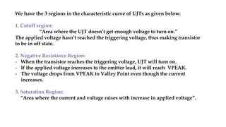
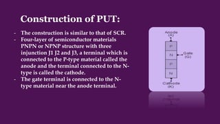
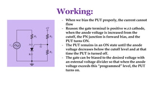
This document provides information about unijunction transistors (UJTs) and programmable unijunction transistors (PUTs). It discusses the construction, working principles, characteristics, and applications of both UJTs and PUTs. Some key points include:
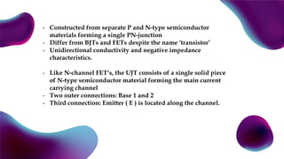
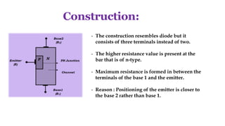
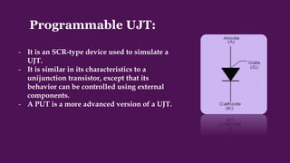
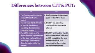
- UJTs and PUTs are three-terminal semiconductor devices that act as electrically controlled switches. UJTs have one PN junction while PUTs have a four-layer PNPN structure.
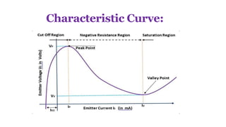
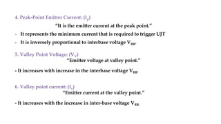
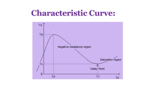
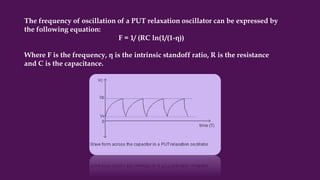
- The characteristic curve of UJTs and PUTs shows different regions including cutoff, negative resistance, and saturation based on the applied voltage. PUTs allow the peak voltage to be programmed using external resistors.
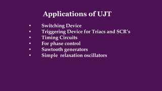
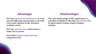
- Common applications of UJ