Transparent Technology By Kiran Sapkale
•Download as PPTX, PDF•
6 likes•1,965 views

This document discusses the development of transparent cellphone technology. It provides details on Polytron Technologies' prototype of a transparent multi-touch display phone using switchable glass technology. The phone appears white and cloudy when powered off but displays images when turned on as liquid crystal molecules realign. Challenges remain around fully integrating batteries and other components. Transparent electronics could enable new applications like see-through displays and help consolidate devices in small spaces. Significant research continues toward developing high-performance transparent materials and improving device performance.

Recommended
More Related Content
What's hot
What's hot (20)
Viewers also liked
Viewers also liked (19)
Similar to Transparent Technology By Kiran Sapkale
Similar to Transparent Technology By Kiran Sapkale (20)
Recently uploaded
Recently uploaded (20)
Transparent Technology By Kiran Sapkale
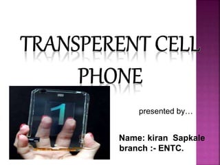
- 1. presented by… Name: kiran Sapkale branch :- ENTC. 1
- 2. The first Transparent transistors were reported in 2003 and display Conventional wisdoms dictates that we will have to wait until between 2013 and 2023 to purchase transparent related merchandise. We contend that transparent technology is technology-in-a-hurry......!!!!
- 3. Its a question that’s been circulating for years, thanks to film like Minority Report and Iron Man 2 that sparks dream of diaphanous mobile future, and more than decade later,its one that’s still without an answer. Sony Ericsson’s Xperia pureness fell that when it hit in the market in 2009.
- 5. Now , Taiwan based Polytron technologies is trying to revive the dream , with a transparent multi touch display that its begun marketing to OEMs . As mobile Geeks reports, the key to polytrons prototype is its so called Switchable Glass technology-a conductive OLED that uses liquid crystal molecules to display images. When the phone is powered off, these molecules from a white cloudy composition , but once activated with electric current , they realign to form texts , icons , or other imagery .
- 7. “IT WILL HAPPEN NEAR THE END OF 2013.TRUST ME.” In its current form , the device still is not totally transparent. Most glaring is the SD card , inserted on the bottom left side of the phone , along side the SIM card. The microphone , camera , and batteries are also visible though polytron plans to hide this with a darker glass cover once it goes to production.
- 9. In an interview with The Verge , Polytron general manager Sam yu acknowledged that the company still working on integrating a smaller , less conspicuous lithium-ion battery . Transparent lithium technology has been in development for some time now , but for the movement , yu’s prototype runs on two small (and very visible) batteries.
- 10. Sam yu told “ It will happen near the end of 2013 “. The looming question , though , is whether or not the market even wants a translucent device. Companies like Samsung , LG , and others have been touting larger transparent displays for years now .
- 11. In its finished state , the phone will feature dual sided multiple displays (Front and back), raising new possibilities for OS and UI design. At this time , however , the display still very much in development . The prototype features no software or operating system , which makes it difficult to visualize in practice .
- 13. The material used in transparent cellphone:- The semiconductor, the electric contacts, and the dielectric layers, must now be invisible – Touch display panels, solar cells, flat panel displays, heaters , ‘smart windows’ .
- 14. Researchers at Oregon State University and Hewlett Packard have reported their first example of an entirely new class of materials which could be used to make transparent transistors that are inexpensive, stable, and environmentally benign. 14 Significant advances in the emerging science of transparent electronics, creating transparent "p-type" semiconductors that have more than 200 times the conductivity of the best materials available for that purpose a few years ago. This basic research is opening the door to new types of electronic circuits that, when deposited onto glass, are literally invisible.
- 16. OLED is nothing but organic light-emitting diode emissive electroluminescent layer is film of organic compound which emits light in response to electric current. This layer of organic is semiconductor is situated between two electrode typically one of this is transperent. OLED’s are used to create digital displays in various devices like mobiles, television, monitors of computer
- 17. OLED’s based on small molecules and those employing polymers. Adding mobile ions to an OLED’s creates light emitting electrochemical cell which is different mode of operation.
- 18. TOUCH PANELS
- 20. **CLEAR ELECTRONICS MAKE YOUR ROOM APPEAR MORE SPACIOUS BY ALLOWING ELECTRONIC DEVICES TO BE CONSOLIDATED AND STACKED IN SMALL SPACES. **THIS TECHNOLOGY COULD ENABLE THE WINDOWS OR MIRRORS IN OUR HOMES TO BE USED AS COMPUTER MONITORS AND TELEVISION SCREENS.
- 21. 3 GOALS TO MOVE AHEAD the first scientific goal of this technology must be to discover, understa and implement transparent high-performance electronic materials. The second goal is their implementation and evaluation in transistor and circuit structures. The third goal relates to achieving application-specific properties since transistor performance and materials property requirements vary, depending on the final product device specifications.
- 23. A NEW REVOLUTION
- 24. 24 APPLICATIONS OF TRANSPARENT CELLPHONE Transparent circuits will have unprecedented applications in flat panel displays and other electronic devices, such as see through display or novel display structures. They have been widely used in a variety of applications like: 1. Antistatic coatings 2. Touch display panels 3. Solar cells, 4. Flat panel displays 5. Heaters 6. Defrosters 7. Optical coatings. and many more….
- 25. 25 MARKET OF TRANSPARENT technology There are four critical aspects of “transparency” that the design and marketing of transparent electronics products needs to focus on for it to become a serious revenue earner. These factors are: • Aesthetics • Integration • Improved economics • Aspects of transparent materials that are not directly related to transparency. .The transparent devices in the market have two challenges to overcome in order to capture the market. They are: • Too cool to succeed • Current apps for transparent electronics are quite primitive. These are the major distraction in the path of these invisible devices…!!!
- 26. 26 Future Scope In the field of solar cells, although much progress has been made in developing new materials and devices for high performance transparent solar cells, there is still plenty of opportunity to study and improve device performance and fabrication techniques compared with the nontransparent solar cell devices. It is likely that new scientific discoveries and technological advances will continue to cross fertilize each other for the foreseeable future.
- 27. The team are also exploring using the resistance properties of their material not just for use in memory but also as a computer processor . This versatility will someday replace memory and central processing units(CPUs)with a single chip that can perform both functions. FUTURE SCOPE much progress has been made in developing new materials and devices for high performance transparent solar cells, there is still plenty of opportunity to study and improve device performance and fabrication techniques compared with the nontransparent solar cell devices.
- 28. 28 CONCLUSION Oxides represent a relatively new class of semiconductor materials applied to active devices, such as TFTs, SWNT transistors. The combination of high field effect mobility and low processing temperature for oxide semiconductors makes them attractive for high performance electronics on flexible plastic substrates. Let us hope that we are soon going to see transparent technology being implemented in our lives…!!!
- 29. FUTURE GADGETS
- 30. What we see in science fiction movies are going to be a real working technology and it is not very far , Competition in the world of technology brings us suprising stuffs that we once dreamed of.
- 32. Boom in electronic gadgets
- 33. That’s all about Transparent Cellphone…!!! Thank you and