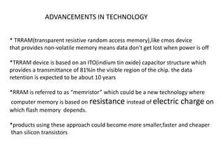
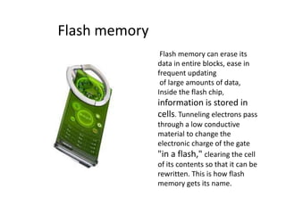
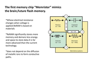
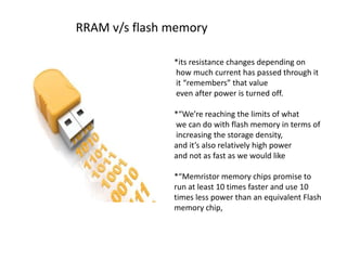
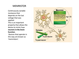
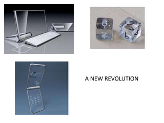
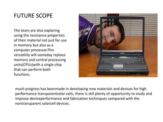
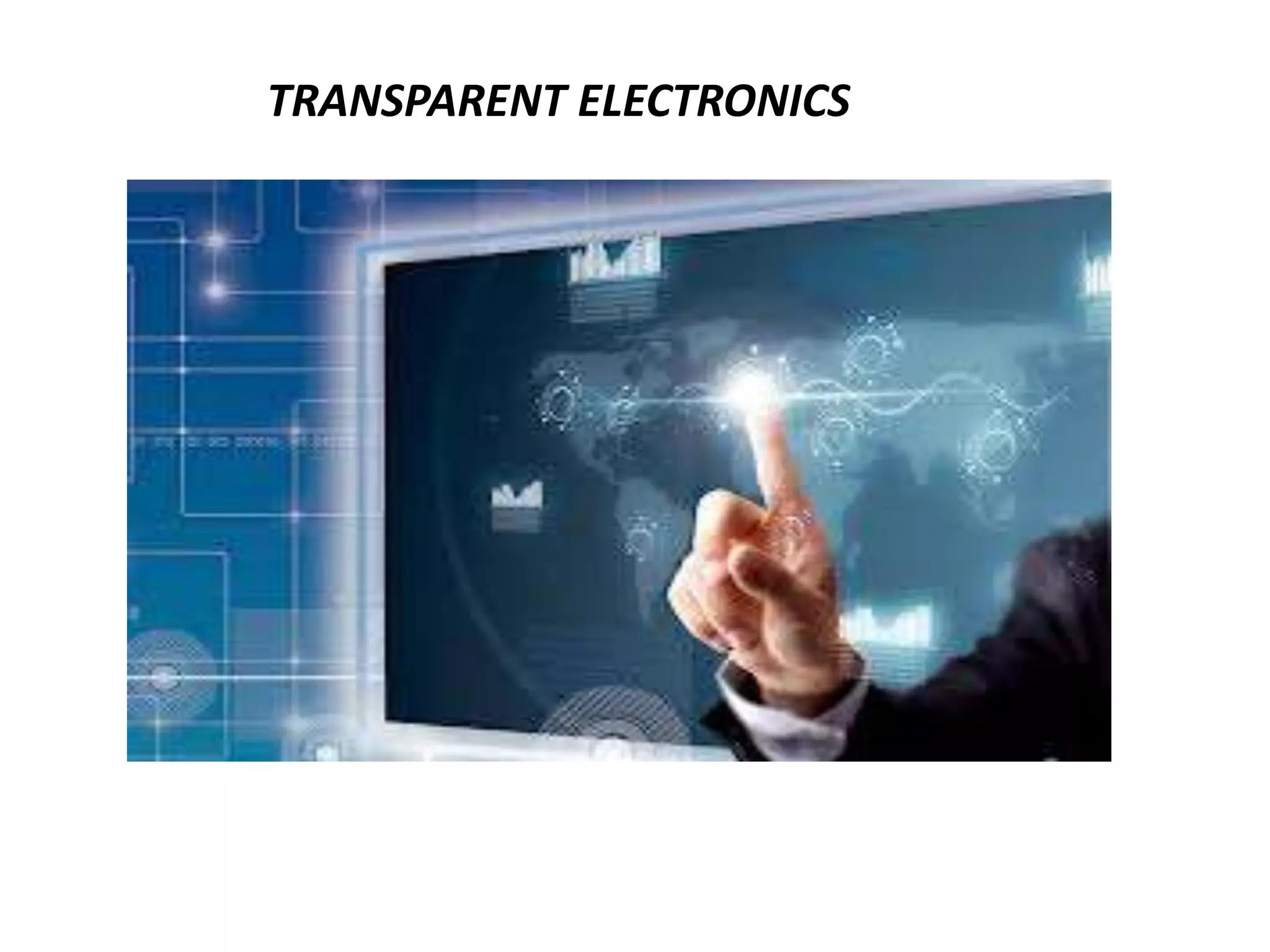
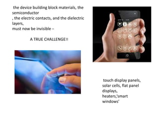
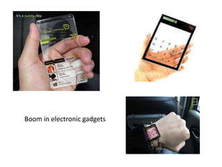
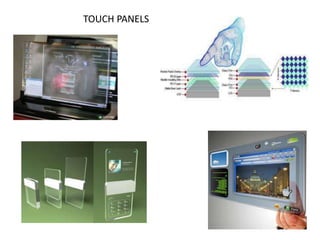
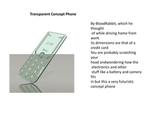
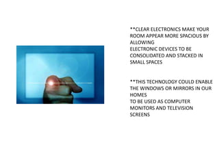
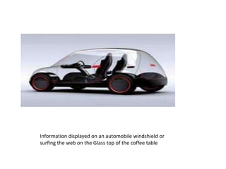
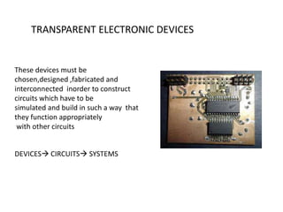
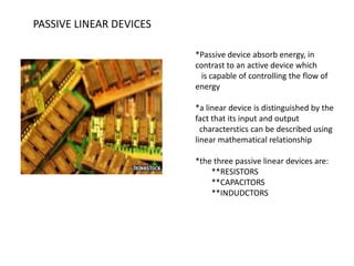
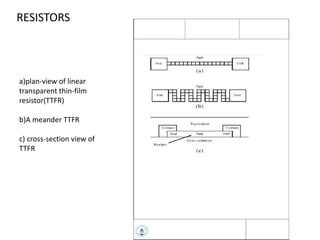
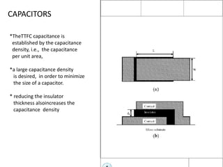
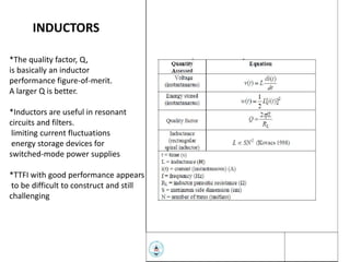
This document discusses the emerging field of transparent electronics. The key goals are to discover transparent, high-performance electronic materials and implement them in transistors, circuits and systems. This would enable applications like touchscreens, solar cells, displays, and smart windows that are transparent. Technologies like transparent thin-film transistors, resistors, capacitors and indutors are discussed. Recent advances include transparent memory devices that could replace flash memory and memristors that mimic the brain's neurons. Future applications may include electronic devices integrated into car windshields, windows, and other transparent surfaces.

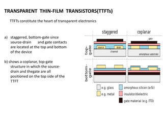
![Ideal n-channel transparent thin
-film transistor (TTFT) operation
(a) Cut- off. Zero drain current
(I D =0)
which is defined by V GS <V ON
(b) Linear, pre-pinch-off.
I D is described by Ohm’s law
[I D =V DS / R C (V GS )] at
low V DS [V DS <<V GS -V ON ]
(c) Nonlinear, pre-pinch-off and,
post- pinch-off, saturation
V DS =V GS -V ON because of the
depletion or ‘pinch- off’](https://image.slidesharecdn.com/transparentelectronicsbykirtikansal-131120105907-phpapp02/85/Transparent-electronics-by-kirti-kansal-20-320.jpg)