Downloaded 1,411 times


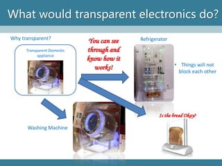


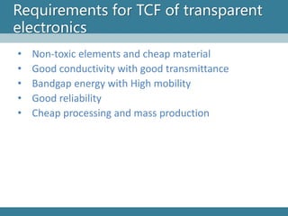


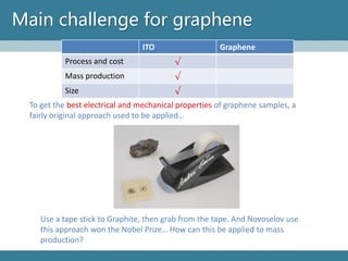
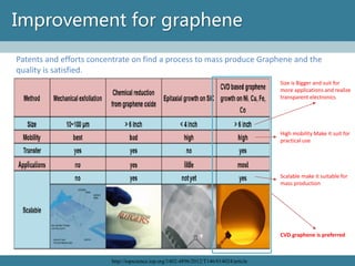


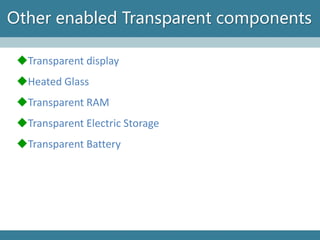


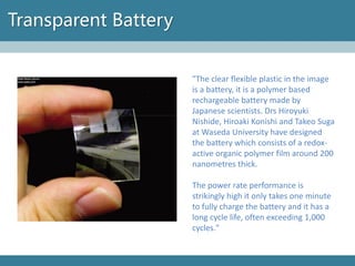

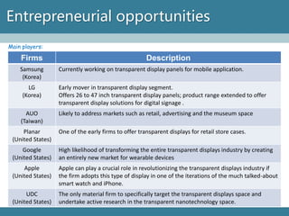


The document discusses the potential and technological advancements of transparent electronics enabled by nanotechnology, highlighting applications in various sectors including domestic appliances, entertainment, architecture, and healthcare. It emphasizes the advantages of materials like graphene and aligned carbon nanotubes in creating efficient transparent electronic components such as displays, batteries, and solar cells. Furthermore, the document identifies entrepreneurial opportunities and key players in the transparent electronics market.


