Downloaded 2,716 times
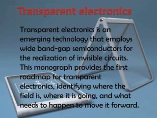


The document discusses transparent electronics and transparent conducting materials. It explains that transparent conductors are neither 100% optically transparent nor metallically conductive due to the contradictory nature of these properties from a band structure perspective. Transparent conducting oxides (TCOs) are commonly used by degenerately doping the material to displace the Fermi level into the conduction band, providing high carrier mobility and low optical absorption. The document also discusses applications of transparent amorphous oxide semiconductors (TAOSs) in displays and chemical detection.


