Download to read offline

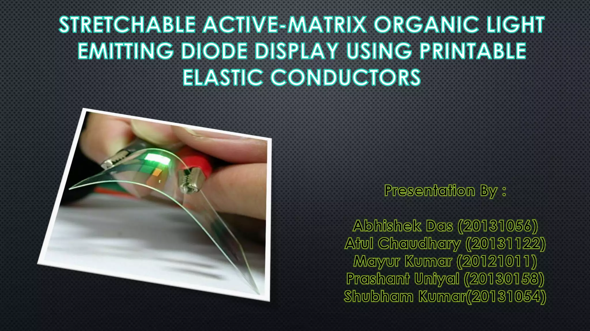
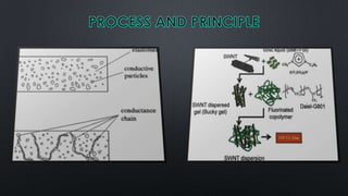


This document summarizes a research article that introduces printable elastic conductors and describes how they can be used to create a stretchable active-matrix organic light emitting diode (OLED) display. The key points are: 1) Printable elastic conductors are produced using a technique that prints conductive inks made of highly elastic fluorinated rubber and dispersed single-walled carbon nanotubes, which allows the conductors to be highly conductive yet stretch over 118%. 2) Using these printable elastic conductors, the authors constructed a stretchable active-matrix OLED display by printing transistors and LEDs on rubber sheets and connecting them via the elastic conductors. 3) This stretchable display technology could enable


