Downloaded 1,899 times
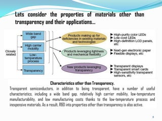
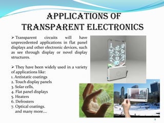
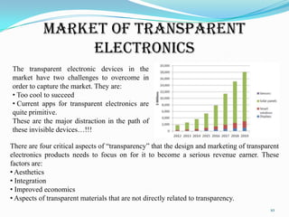
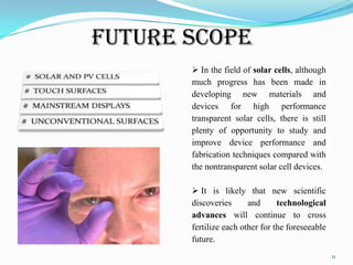


Transparent electronics is an emerging technology that uses wide band-gap semiconductors to create invisible circuits and optoelectronic devices. The goal is to develop transparent materials with high performance and electrical conductivity that can be implemented in transistors and circuits. Transparent oxide semiconductors like zinc oxide and amorphous indium gallium zinc oxide are being researched for use in transparent transistors and devices. Potential applications include see-through displays, touchscreens, solar cells, and other electronic devices that are transparent when deposited on glass. While progress is being made, transparent electronics still face challenges in fully capturing markets due to limitations in current applications and high manufacturing costs.


