Downloaded 222 times


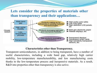
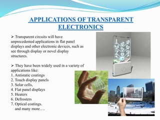


The document discusses transparent electronics, which uses wide bandgap semiconductors to create invisible circuits and optoelectronic devices. It describes how transparent oxide semiconductors like indium oxide, tin oxide, and zinc oxide combine high conductivity with high visual transparency. Transparent thin-film transistors and recent advances in "p-type" semiconductors are enabling new types of electronic circuits that can be deposited on glass and are literally invisible. Potential applications of transparent electronics include see-through displays, touchscreens, solar cells, and heaters. Continued research aims to improve performance and fabrication techniques to bring this emerging technology into more widespread use.


