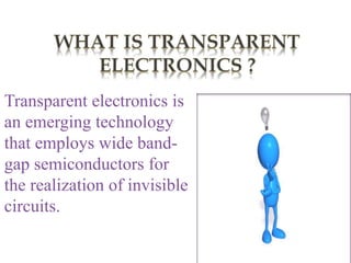
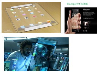
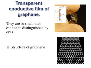
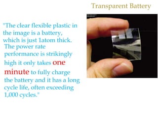
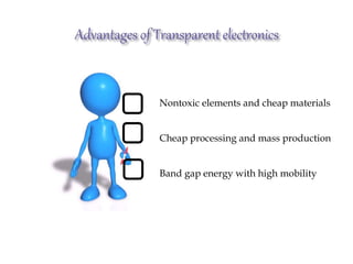
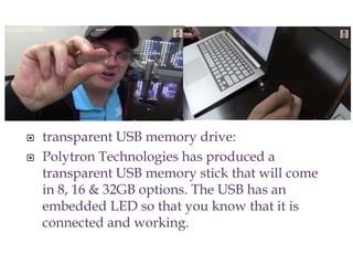
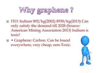
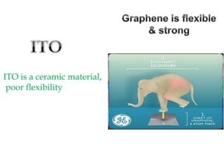
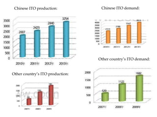
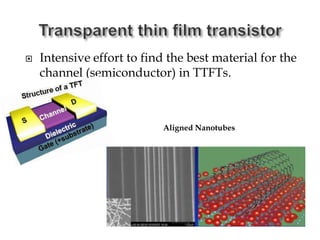
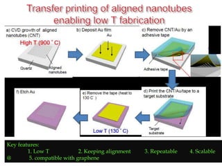
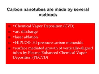
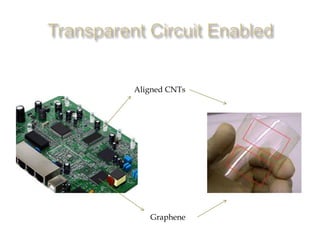
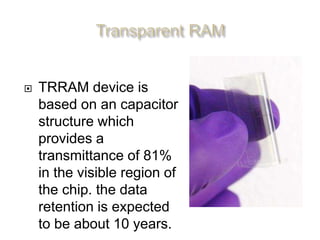
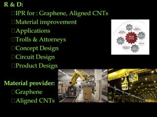
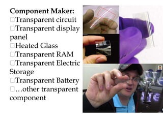
This are the slides about transparent electronics explaining the importance of graphene and enabling the possibility of all electronics devices as transparent.
Transparent electronics uses transparent materials to replace opaque semiconductor materials typically used in electronic device fabrication. This document discusses the basic principles and materials used for transparent electronics, including transparent conducting oxides and thin film transistors. A key enabling technology is graphene, which conducts heat and electricity efficiently while being nearly transparent. Transparent electronic devices have applications in domestic appliances, entertainment, communication, architecture, healthcare, and industry due to advantages like invisibility and flexibility.
TRANSPARENT ELECTRONICS
Abstract: Transparent electronics is an emerging science and technology field focused on producing ‘invisible’ electronic circuitry and opto-electronic devices.
Applications include consumer electronics, new energy sources, and transportation; for example, automobilewindshields could transmit visual information to the driver. Glass in almost any setting could also double as an electronic device, possibly improving security systems or offering transparent displays. In a similar vein, windows could be used to produce electrical power. Other civilian and military applications in this research field include realtime wearable displays.
As for conventional Si/III–V-based electronics, the basic device structure is based on semiconductor junctions and transistors. However, the device building block materials, the semiconductor, the electric contacts, and the ielectric/passivation layers, must now be transparent in the visible –a true challenge! Therefore, the first scientific goal of this technology must be to discover,understand, and implement transparent high-performance electronic materials. The second goal is their implementation and evaluation in transistor and circuit structures.
The electronics during the past 10 years, the classes of materials available for transparent electronics applications have grown dramatically. Historically, this area was dominated by transparent conducting oxides (oxide materials that are both electrically conductive and optically transparent) because of their wide use in antistatic coatings, touch display panels, solar cells, flat panel displays, heaters, defrosters, ‘smart windows’ and optical coatings. All these applications use transparent conductive oxides as passive electrical or optical coatings. The field of transparent conducting oxide (TCO) materials has been reviewed and many treatises on the topic are available. However, more recently there have been tremendous efforts to develop new active materials for functional transparent electronics. These new technologies will require new materials sets, in addition to the TCO component, including conducting, dielectric and semiconducting materials, as well as passive components for full device fabrication.
COMBINING OPTICAL TRANSPARENCY WITH ELECTRICAL CONDUCTIVITY
Transparent conductors are neither 100% optically transparent nor metallically conductive. From the band structure point of view, the combination of the two properties in the same material is contradictory: a transparent material is an insulator which possesses completely filled valence and empty conduction bands; whereas metallic conductivity appears when the Fermi level lies within a band with a large density of states to provide high carrier concentration. Efficient transparent conductors find their niche in a compromise between a sufficient transmission within the visible spectral range and a moderate but useful in practice electrical conductivity.
Transparent electronics is an emerging science and technology field concentrates on producing ‘invisible’ electronics circuit and optoelectronics devices. The application contains consumer electronics such as automobile windshield, transparent solar panel, transparent display and real time wearable display. In the conventional Si/III-V based electronics, the structure is based on semiconductor junction & transistor. However, the basic building material for transparent electronic devices which is to be transparent and in visible range is a true challenge. Therefore, to understand and implement such technology there are two scientific goals, to have a material which are optically transparent and electrically conductive and to implement an invisible circuitry. Development of such invisible transparent electronic devices needs expertise together from pure and applied science, material science, chemistry, physics &electronic science.
Transparent electronics is an emerging technology that employs wide band-gap semiconductors for the realization of invisible electronics circuits and optoelectronics devices.
The document discusses transparent electronics, which uses wide bandgap semiconductors to create invisible circuits and optoelectronic devices. It describes how transparent oxide semiconductors like indium oxide, tin oxide, and zinc oxide combine high conductivity with high visual transparency. Transparent thin-film transistors and recent advances in "p-type" semiconductors are enabling new types of electronic circuits that can be deposited on glass and are literally invisible. Potential applications of transparent electronics include see-through displays, touchscreens, solar cells, and heaters. Continued research aims to improve performance and fabrication techniques to bring this emerging technology into more widespread use.
This document provides an overview of transparent electronics as presented in a student's seminar report. It includes an introduction to transparent electronics, a brief history covering transparent conductive oxides and thin-film transistors, and how transparent electronic devices work utilizing oxide semiconductors. The document consists of the student's seminar report covering topics such as advancements, applications, markets, and future scope of transparent electronics. It is presented to fulfill the requirements for a Bachelor of Technology degree.
this a presentation on transparent electronics. check out a really wonderful technology evolved in...............
Presented by :
1. ISLAM MD RAISUL 13-23674-1
2. HASAN,RAKIB-UL 13-23538-1
3. AZAM MD. AKIBUL 13-23680-1
4. RAHMAN MD. RIFAT 13-23747-1
5. RAHMAN ASHIKUR 13-23293-1
AIUB (EEE)
Course Name : POWER STATION
Transparent electronics use wide band gap semiconductors like oxide semiconductors that are both highly conductive and transparent. Researchers at Oregon State University pioneered the use of zinc tin oxide, an inexpensive and environmentally friendly material, for resistive random access memory (RRAM) or "memristors." Memristors can store data through electrical resistance instead of electron charge and could replace flash memory. Transparent electronics open up possibilities for innovative new products like information displayed on windshields or web browsing on coffee tables.
The document discusses transparent electronics, which uses invisible electronic circuitry and optoelectronic devices. It describes applications like smart car windshields and solar panel embedded windows. Transparent conducting oxides are key materials that are engineered to be both transparent and conductive through doping and modifying the band gap. Circuits can be made through transparent thin film resistors, capacitors, and transistors. Further research is still needed to improve the accuracy of transparent thin film resistors.
This document discusses transparent electronics, which employs wide band-gap semiconductors like zinc oxide and amorphous indium gallium zinc oxide to create invisible electronic circuits and optoelectronic devices. These oxide semiconductors combine high visual transparency with high or low conductivity. Transparent oxide transistors have been made using zinc oxide channels. Key applications of transparent electronics include transparent passive devices, transparent active devices, security, entertainment, and more efficient energy utilization. The technology holds promise for impacting human-machine interaction and reducing environmental pollution from traditional techniques.
This document discusses the development of transparent cellphone technology. It provides details on Polytron Technologies' prototype of a transparent multi-touch display phone using switchable glass technology. The phone appears white and cloudy when powered off but displays images when turned on as liquid crystal molecules realign. Challenges remain around fully integrating batteries and other components. Transparent electronics could enable new applications like see-through displays and help consolidate devices in small spaces. Significant research continues toward developing high-performance transparent materials and improving device performance.
The document discusses transparent electronics and their potential applications. It explains that new technologies enable optoelectronic devices and wide band-gap semiconductors to realize invisible circuits. Key materials like zinc oxide and amorphous oxides allow for transparent thin-film transistors, resistors, capacitors and inductors. The transparent circuits can be made very small, light, and integrated into touch surfaces, displays, solar cells, and other unconventional surfaces. The document provides references for further information on transparent electronics.
The document discusses transparent electronics and transparent conducting materials. It explains that transparent conductors are neither 100% optically transparent nor metallically conductive due to the contradictory nature of these properties from a band structure perspective. Transparent conducting oxides (TCOs) are commonly used by degenerately doping the material to displace the Fermi level into the conduction band, providing high carrier mobility and low optical absorption. The document also discusses applications of transparent amorphous oxide semiconductors (TAOSs) in displays and chemical detection.
This document outlines research on transparent conducting oxides (TCOs). It discusses how combining optical transparency with electrical conductivity is achieved through degenerate doping and the Burstein-Moss shift. TCOs made of materials like indium oxide, tin oxide, cadmium oxide and zinc oxide are used to create transparent electronic devices through carrier generation via substitutional doping or oxygen reduction. Applications include use in mobile phones, laptops, solar panels, and potential future uses like solar windows.
This document discusses transparent electronics. Transparent electronics are materials that are both optically transparent and electrically conductive. Common transparent conducting oxides used include indium oxide, zinc oxide, and cadmium oxide. These materials can be fabricated using methods like sputtering, evaporation, chemical vapor deposition, and pulsed laser deposition. Transparent electronics have applications in devices like transparent thin-film transistors and UV detectors. Additional applications discussed include uses in OLED displays, transparent solar panels, and other domestic, entertainment, communication, architecture, healthcare, and industrial applications.
Transparent electronics is an emerging technology that uses wide band-gap semiconductors to create invisible circuits and optoelectronic devices. The goal is to develop transparent materials with high performance and electrical conductivity that can be implemented in transistors and circuits. Transparent oxide semiconductors like zinc oxide and amorphous indium gallium zinc oxide are being researched for use in transparent transistors and devices. Potential applications include see-through displays, touchscreens, solar cells, and other electronic devices that are transparent when deposited on glass. While progress is being made, transparent electronics still face challenges in fully capturing markets due to limitations in current applications and high manufacturing costs.
Transparent electronics is an emerging field focused on producing transparent electronic devices using transparent materials instead of opaque semiconductors. Transparent conducting oxides (TCOs) like indium tin oxide are materials that have both optical transparency and electrical conductivity properties that are key for transparent electronics. Transparent electronics devices include transparent thin-film transistors and can be used for applications like see-through displays, solar windows, and invisible cameras and RFIDs.
This document discusses transparent electronics using transparent conducting oxides (TCOs). It introduces TCOs such as indium tin oxide which allow for both optical transparency and electrical conductivity. This is achieved through degenerate doping and the Burstein-Moss shift. TCOs find applications in transparent thin-film transistors, resistors, capacitors and indutors which could enable see-through laptops, phones and solar panels. Further advances could lead to solar windows but also environmental challenges.
Transparent electronics allow electronic devices like phones, windows, and displays to function while maintaining transparency. This is achieved using materials like zinc oxide and amorphous indium gallium zinc oxide that conduct electricity yet transmit visible light. Potential applications include see-through displays, touchscreens, solar cells, and heaters that are optically clear. Advancements continue to be made in improving device performance and expanding uses of transparent electronics in areas like displays, photovoltaics, and unconventional surfaces.
Transparent Electronic PPT
Transparent electronics is an emerging science and technology field focused on producing ‘invisible’ electronic circuitry and opto-electronic devices. Applications include consumer electronics, new energy sources, and transportation; for example, automobile windshields could transmit visual information to the driver. Glass in almost any setting could also double as an electronic device, possibly improving security systems or offering transparent displays. In a similar vein, windows could be used to produce electrical power. Other civilian and military applications in this research field include realtime wearable displays. As for conventional Si/III–V-based electronics, the basic device structure is based on semiconductor junctions and transistors. However, the device building block materials, the semiconductor, the electric contacts, and the dielectric/passivation layers, must now be transparent in the visible –a true challenge! Therefore, the first scientific goal of this technology must be to discover, understand, and implement transparent high-performance electronic materials. The second goal is their implementation and evaluation in transistor and circuit structures. The third goal relates to achieving application-specific properties since transistor performance and materials property requirements vary, depending on the final product device specifications. Consequently, to enable this revolutionary technology requires bringing together expertise from various pure and applied sciences, including materials science, chemistry, physics, electrical/electronic/circuit engineering, and display science.
This document provides an introduction to transparent electronics. It discusses how transparent electronics allows for invisible electronic circuitry and devices with applications in consumer electronics, energy, and transportation. The basic device structure is similar to conventional electronics, but the materials must be transparent in the visible spectrum. The goals of transparent electronics are to discover and implement transparent electronic materials, incorporate these materials into transistor and circuit designs, and achieve application-specific performance requirements. Realizing this technology requires expertise from various fields including materials science, chemistry, physics, and engineering. In the past decade, the available materials for transparent electronics have expanded beyond transparent conducting oxides to include other conducting, dielectric, and semiconducting materials needed for full device fabrication.
These slides use concepts from my (Jeff Funk) course entitled analyzing hi-tech opportunities to analyze how transparent electronics are becoming economic feasible. Transparent electronics can turn windows into displays and solar cells and enable more aesthetically pleasing designs. Home, car, and office windows can be used to display information or absorb solar energy. The former is also applicable to contact lenses and glasses. Transparent electronics can also enable new forms of designs such as transparent phones, appliances, and monitors. Improvements in transparent conductive films such as indium tin oxides, other forms of oxides, and graphene enable these transparent displays.
Special optical fibers and fiber capillaries coated with Indium-Tin-OxideVoloda
This document discusses the preparation and characterization of Indium-Tin-Oxide (ITO) thin films deposited on planar substrates and optical fibers using a dip-coating method. ITO films were prepared from a colloidal solution and characterized electrically and optically. The resistivity of ITO films on planar substrates was 0.11 ohm-mm but increased to 150 megohms on optical fibers. The ITO films had a high porosity of 54% and refractive index of 1.457. ITO coatings were deposited successfully inside capillaries and on optical fibers using this simple dip-coating preparation method.
This document discusses transparent electronics and transparent conducting oxides (TCOs). It introduces TCOs like indium oxide and zinc oxide, which enable invisible electronics by combining optical transparency with electrical conductivity. It explains how doping and oxygen reduction can generate carriers in TCOs to produce this unique combination of properties. Potential applications mentioned include mobile phones, laptops, solar panels, and transparent displays. The document concludes that transparent electronics will have a great impact on human-machine interaction and lead to new applications, while also potentially posing environmental challenges.
The document provides an overview of organic light emitting diodes (OLEDs). It discusses the history and development of OLEDs, including key discoveries and commercialization milestones. The structure, working principle, materials, fabrication processes, and types of OLED displays are described. Characteristics such as contrast ratio, color gamut, response time and viewing angle are compared between OLED and LCD displays. Advantages of OLEDs include being self-luminous, thin, flexible and having high brightness and contrast, while limitations include short lifetimes and degradation from oxygen and water.
Transparent electronics by kirti kansalTechnocratz
This document discusses the emerging field of transparent electronics. The key goals are to discover transparent, high-performance electronic materials and implement them in transistors, circuits and systems. This would enable applications like touchscreens, solar cells, displays, and smart windows that are transparent. Technologies like transparent thin-film transistors, resistors, capacitors and indutors are discussed. Recent advances include transparent memory devices that could replace flash memory and memristors that mimic the brain's neurons. Future applications may include electronic devices integrated into car windshields, windows, and other transparent surfaces.
This document provides an overview of nanotechnology and discusses several applications of nanotechnology including graphene, carbon nanotubes, transparent and flexible electronics, printed electronics, batteries, solar energy and more. It defines nanotechnology as engineering at a very small scale, below 100 nanometers. Carbon nanotubes are described as tubular cylinders of carbon atoms that have extraordinary electrical, mechanical and thermal properties. Graphene is a one atom thick sheet of carbon atoms arranged in a honeycomb lattice that has potential applications in integrated circuits, transparent electrodes and other devices.
The structure of the C-C complex in silicon has been debated since long time. Different theoretical and experimental studies tried to shed light on the properties of these defects that are at the origin of the light emitting G-center. It is essential to understand structural and electronic properties of
these defects because they are relevant for applications in lasing and there is an increasing interest
to control their formation and concentration in bulk silicon. In this paper, we study structural, electronic, and optical properties of different possible configurations of the C-C complex in bulk
silicon by means of density functional theory (DFT) plus many-body perturbation theory (MBPT).
Our finding show that different competing structures could be at the origin of the experimental results.
Organic transistors were first developed in 1986 and use organic molecules rather than silicon as the active material. They have advantages over traditional silicon transistors such as being lightweight, flexible, cheap to produce, and compatible with solution processing and plastic substrates. Key parameters for organic transistors include mobility, on-off ratio, and threshold voltage. Device design can be top contact or bottom contact, with top contact having superior performance. Pentacene-based organic transistors currently have the best field effect mobility. Improving the dielectric, electrodes, and reducing contact resistance and leakage current can further increase performance. Organic transistors have applications in flexible displays, memory, sensors, and more.
1) The document discusses direct and indirect semiconductors, explaining that direct semiconductors have a minimum energy (Eg) that occurs at the same crystal momentum (k) while indirect semiconductors have a minimum energy (Eg) that occurs at different k values.
2) It also covers effective mass, which is used instead of free electron mass when applying equations of electrodynamics to charge carriers in solids. Effective mass depends on the curvature of the energy-momentum relationship.
3) The document describes how electrons and holes behave as quantum particles when confined in a thin semiconductor layer between barriers of a different semiconductor, resulting in discrete energy levels instead of a continuum.
This ppt is about semiconductor diodes.You can get every basic information about PN junction diode and its working and some more information about the semiconductors.
A photovoltaic (PV) module is a packaged, connected assembly of solar cells that can be used to generate electricity in commercial and residential applications. It consists of interconnected solar cells, and multiple modules can be connected to form a larger PV system. Reasons to install PV modules include concerns for the environment, cost savings, and expectations of future increased energy costs. PV systems have three main components - PV modules or solar arrays, the balance of system equipment, and electrical loads. PV modules can be used in stand-alone systems, grid-connected systems, or hybrid systems combined with other power sources. Transparent solar modules can also be used as building-integrated photovoltaics in windows, roofs, and
These slides use concepts from my (Jeff Funk) course entitled Biz Models for Hi-Tech Products to analyze the business model for Transparent and Flexible Displays. Transparent displays provide new forms of value to users particularly in the form of better augmented reality. They also make bi-direction games and other forms of communication and entertainment possible. They can be used in tablet computers, mobile phones, and other electronic devices by tech junkies and other potential users. These slides also explain other aspects of the business model such as the method of value capture, scope of activities, and method of strategic control.
This document provides an overview of supercapacitors. It discusses what supercapacitors are, their history, basic design involving two electrodes separated by an ion permeable membrane, how they work by forming an electric double layer when charged, the materials used such as carbon nanotubes for electrodes and electrolytes, their features like high energy storage and charge/discharge rates, applications including use in buses and backup power systems, and advantages like long lifespan and eco-friendliness with disadvantages like low energy density and high cost.
Organic Thin Film Transistor 2016: Flexible Displays and Other Applications 2...Yole Developpement
Are OTFTs ready to disrupt the display industry and enable fully-flexible devices?
ORGANIC TFTS ARE ENTERING THE FAB BY THE BACK DOOR
When trying to build a flexible display panel, the Thin Film Transistor (TFT) matrix is one of the most challenging and fragile functional layers.
Interest in OTFT emerged in the mid-2000s when mobility reached values similar to amorphous silicon (a-Si), the dominant display backplane technology. This triggered a flurry of activity at leading display manufacturers, and prototypes rapidly emerged. Besides fast-improving electrical performance, OTFT’s intrinsic flexibility made the technology ideal for the realization of flexible displays. In 2007, the first ever flexible AMOLED panel was demonstrated by Sony and featured an organic TFT.
However, interest waned as performance and homogeneity issues persisted, and other TFT technologies like LTPS and metal oxide emerged.
Nevertheless, organic semiconductor companies kept perfecting their molecules and ink formulations, gaining a better understanding of the interaction between the materials, the transistor structure, and the manufacturing process. Consequently, performance in the lab improved by another order of magnitude. Combined with the explosive growth of flexible displays and the promise of a cost-efficient, solution-based manufacturing process, interest in OTFT has renewed.
Panel makers remain cautious, but a handful in Taiwan and China are currently attempting to retrofit older Gen 2.5 - 4.5 fabs with OTFT. These first attempts to move OTFT into mass production will be critical for the technology’s future. Failure in these initial industrialization attempts could be fatal for the OTFT industry, or, at the very least, set it back many years. However, if OTFT proves that it can be mass produced and enables panel makers to revive those obsolete fabs with high-margin flexible displays, there are no fundamental barriers prohibiting the technology from being quickly scaled up to fabs Gen 8 or above, and possibly challenge the vast market for traditional a-Si based panels like LCD TV, monitors, etc. In the long-term, because they are inherently solution-processable, OTFTs are also an ideal backplane candidate for additive manufacturing and fully printed displays.
More information on that report at http://www.i-micronews.com/reports.html
Semiconductor Physics
In 3 sentences:
Semiconductors have electrical properties between metals and insulators, with conductivities from 10-4 to 104 S/m. Their crystal structure leads to electrons being able to move between valence and conduction bands, making semiconductors bipolar with both electrons and holes conducting. Semiconductors are classified as intrinsic, with equal electron and hole concentrations determined by temperature, or extrinsic with additional carriers from dopant impurities making them either n-type or p-type.
This document summarizes key concepts about semiconductors including:
1) Semiconductors have electrical properties that can be controlled through doping with impurities, allowing them to be used in transistors and integrated circuits. Their purity must be very high, measured in parts per billion.
2) Intrinsic semiconductors like silicon have a band gap between the valence and conduction bands that requires energy like heat or light to excite electrons across.
3) Extrinsic semiconductors are doped with impurities that introduce electrons (n-type) or holes (p-type) that determine the semiconductor's conductivity type and shift the Fermi level. Charge neutrality must be maintained.
Supercapacitors can store more energy than regular capacitors through electrochemical double layer capacitance. They provide very high charge/discharge rates, long cycle life, and high efficiency. While supercapacitors have lower energy density than batteries, they compensate with much higher power density and longer lifespan. Applications include public transportation, hybrid electric vehicles, backup power systems, and consumer electronics where high power delivery is needed.
How to Become a Thought Leader in Your NicheLeslie Samuel
Are bloggers thought leaders? Here are some tips on how you can become one. Provide great value, put awesome content out there on a regular basis, and help others.
Future possibility -nanotextiles for automotiveShubham Patil
This document discusses potential future applications of nanotextiles in the automotive industry. It outlines goals of making cars lighter, more efficient and with more interior space. Methods of producing carbon nanotubes are described and their properties explained, making them suitable for solar cell composites and speakers. The document discusses using carbon nanotube composites for car body panels that could store energy and for transparent solar cells on windows. Integrating carbon nanotube speakers into car interiors to reduce weight and complexity is also proposed. Bibliography sources on these potential applications are provided.
Transparent electronics use materials that allow light to pass through while still functioning as electronic devices. They have applications in displays, solar cells, and other devices. Key materials include transparent conductive oxides and thin-film transistors deposited on glass. Advancements have increased conductivity over 200 times. Transparent electronics could enable see-through displays and novel display structures, with challenges remaining in applications and market capture.
Graphene has potential advantages for smartphone batteries and components. It allows for batteries with higher energy density, faster charging, and improved heat dissipation for processors. However, research also shows graphene can be toxic, as its jagged edges easily pierce cell membranes. While graphene shows promising properties, more study is still needed on both benefits and risks due to its developmental stage.
Transparent electronics is an emerging technology that uses wide band-gap semiconductors to create invisible circuits. It employs transparent conductive oxides and thin-film transistors, with zinc oxide and amorphous indium gallium zinc oxide being particularly useful due to their high transparency and electrical conductivity. Transparent electronics has applications in areas like flat panel displays, see-through displays, touch screens, and solar cells. However, manufacturing processes remain expensive and lifetimes are shorter than non-transparent devices. Further research could improve performance and lower costs.
A paper battery is a flexible, ultra-thin energy storage and production device formed by
combining carbon nanotubes with a conventional sheet of cellulose-based paper.
Characteristics and applications of graphenealfachemistry
(1) Graphene is a single layer of carbon atoms in a tightly packed honeycomb crystal structure that is only one atom thick, making it the thinnest material known. It has many desirable properties including high strength, conductivity, and surface area. (2) Potential applications of graphene include use in electronics to replace silicon in integrated circuits, use in supercapacitors for energy storage, use in touchscreens and displays to replace indium tin oxide, and use as an additive to strengthen materials like cement and plastic. (3) While graphene research has led to many potential applications, mass production of consistent, high-quality graphene remains a challenge that must still be overcome for widespread commercial use.
This document summarizes a presentation on innovations in clean mobility materials. It discusses key developments in battery materials and fuel cells that can increase the driving range of electric vehicles. Regarding batteries, it outlines strategies to optimize cathode materials, shift to silicon-based anodes, and enable high nickel cathode compositions in large pouch cells. It also discusses the potential of solid state batteries. For fuel cells, it notes their advantages over electric vehicles and key challenges of reducing costs and building out hydrogen infrastructure.
Flexible electronic components like resistors, capacitors, memories, amplifiers, and batteries are being developed that can operate on flexible substrates. Transferable silicon nanomembranes provide advantages for flexible electronics due to their high speed and mobility. Researchers have demonstrated circuits like SRAM memory and ring oscillators on flexible plastic substrates using extremely thin silicon layers. Flexible lithium ion batteries and supercapacitors have also been developed using carbon nanotubes and organic electrolytes. Flexible electrophoretic displays are being commercialized for applications like signs, mobile phones, and automobiles by leveraging their strong contrast, low power usage, and potential for large areas. Further progress is needed in areas like higher refresh rates and full color capabilities.
Flexible organic LEDs consist of small molecule OLEDs or polymer OLEDs and have several advantages over traditional LEDs. They can be produced through printing or coating processes, allowing for thin, lightweight, and flexible designs. Flexible OLEDs provide vibrant colors, high contrast, wide viewing angles, low power consumption, and can be manufactured cost effectively. However, challenges remain in improving the lifetime and efficiency of blue OLEDs to match red and green OLEDs. Potential applications include small-molecule and polymer OLED displays for devices like phones, tablets and signs due to their thin, flexible designs.
Researchers at Oregon State University have discovered a new class of materials called amorphous heavy-metal cation multicomponent oxides that could enable transparent transistors. These inexpensive, stable, and eco-friendly materials could lead to new industries and consumer products like cheap disposable electronics, improved screens, or flexible electronics. Transparent electronics uses transparent semiconductors instead of opaque materials, allowing for invisible circuits. This emerging technology relies on transparent conducting oxides and thin film transistors.
Organic electronics is an emerging field with an unimaginable future.I have included nutshell of applications and future scope in this field.Think it will be helpful for engineering aspirants.
Can we just imagine of having a TV which can be rolled up? Wouldn’t you like to be able to read off the screen of your laptop in direct sunlight? Your mobile phone battery to last much, much longer? Or your next flat screen TV to be less expensive, much flatter, and even flexible? Well, now it is possible by an emerging technology based on the revolutionary discovery that, light emitting, fast switching diode could be made from polymers as well as semiconductors.OLED
Graphene materials for opto and electronic applications 2014 Report by Yole D...Yole Developpement
What is the industrial potential behind the graphene academic R&D hype?
$141M GRAPHENE MATERIALS MARKET IN 2024 WILL BE DRIVEN MAINLY BY TRANSPARENT CONDUCTIVE ELECTRODES AND ENERGY STORAGE APPLICATIONS
Graphene is a two-dimensional (2D) material with exceptional properties, such as ultrahigh electrical and thermal conductivities, wide-range optical transmittance and excellent mechanical strength and flexibility. These properties make it a promising material for emerging and existing applications in printed & flexible circuitry, ultrafast transistors, touch screens, advanced batteries and supercapacitors, ultrafast lasers, photodetectors and many other non-electronic applications.
Although graphene technology is still in its infancy, remarkable progress has been made in the last few years developing graphene production methods. Numerous opto and electronic devices based on graphene have been demonstrated on lab-scale models. However, the numerous challenges of graphene technology should not be underestimated. The lack of bandgap in graphene is its key fundamental challenge. Other technology challenges are related to the development of industrial methods to produce graphene with high and consistent quality at acceptable costs.
Although today there is no graphene-based electronic application in mass production, several companies already offer commercially graphene materials. The graphene material market value in 2013 was about $11 million, represented principally by the demand for the R&D and prototyping. Two scenarios for the future market growth are presented in the report. According to the base scenario, the global annual market value for graphene materials in opto and electronic applications will reach $141 million in 2024, featuring a 2013-2019 CAGR of 18.5%. Accelerated market growth is expected after 2019, with a 2019-2024 CAGR of 35.7%. In 2024, the graphene material market will be represented mainly by the demand for transparent conductive electrodes and advanced batteries and supercapacitors.
HOW CAN GRAPHENE TECHNOLOGY CHALLENGES AND APPLICATION POTENTIAL BE TRANSFORMED INTO BUSINESS OPPORTUNITIES?
In order to reach the best possible performance on lab-scale devices, high quality materials are required. Material suppliers able to consistently deliver high-quality materials have a competitive advantage on the graphene market.
The booming interest in graphene technologies has led to a high demand on graphene equipment. As shown in the report, CVD equipment makers today mainly focus on the R&D equipment used to produce high-quality graphene.
More information on that report at http://www.i-micronews.com/reports/Graphene-materials-opto-electronic-applications/3/416/
IRJET - Review on Ameliorated in the Life, and Calibrated the OledIRJET Journal
This document summarizes research on improving the lifespan of OLED (organic light-emitting diode) displays. It discusses how OLED degradation occurs through chemical breakdown processes involving radical species. Methods to improve OLED lifetime are proposed, including using thermally activated delayed fluorescent materials and adding a thin lithium-containing layer. The document also reviews the structure and functioning of OLEDs, different degradation mechanisms, and potential future applications and challenges of OLED technology.
Paper batteries are flexible, ultra-thin energy storage devices made by combining carbon nanotubes with paper. They function as both batteries and supercapacitors. Carbon nanotubes coated onto stainless steel substrates are used as electrodes, which are layered with electrolytes and separated by paper. During discharge, electrons flow from the negative to positive terminals through the electrolytes. Paper batteries are cost-effective, flexible, lightweight and can be mass produced. However, carbon nanotube production is currently expensive and inefficient.
Conformal electronics and their economic feasiblityJeffrey Funk
These slides use concepts from my (Jeff Funk) course entitled analyzing hi-tech opportunities to analyze how the economic feasibility of conformal electronics is becoming better through using thinner materials, an island-bridge design, and Moore’s Law. The island-bridge design is a mesh of islands containing somewhat rigid components that are connected by mesh of stretchable materials. This enables electronics to be more effectively used in space-restricted places, in skin patches, and next to human organs. Transfer printing, which is a form of roll-to roll printing, enables the costs to be relatively low.
I think it will help the beginners who are much not aware of this topic.This is a complete presentation about organic electronics.That have contain all the topics which i think would be very helpful mostly for engineering students and there are many pictures and no names in the slides so students can easily download it and paste it for their college presentation.
The document discusses polymer light-emitting diodes (PLEDs) which emit light when a voltage is applied. PLEDs consist of a thin film of semiconducting polymer sandwiched between electrodes. When electrons and holes are injected, their recombination causes light emission. PLEDs have advantages over LCDs and CRTs like lower cost, smaller size, flexibility, and lower power requirements. Potential applications include flexible displays, wearable displays, and camouflage materials that can change patterns.
Features foldable electronics
I know perfectly that many people could think: Hey guy, this stuff is only a dream, good for some sci-fi movies.
This general opinion is normal because so far we have seen electronics always opaque but, before show these project, I wanted to be sure they were feasible.
Well, if you read the ebook " A foldable world" - http://www.biodomotica.com/foldable-nanotech.htm - you will find that all this is true.
Most important universities, companies and research centers around the world are working on nanotechnology and on projects that I like: transparent electronics.
You don't need a Ph.D. in Physics to understand articles inside the ebook. At the end of reading you will begin to ask for a new foldable & transparent laptop ;-)
These devices are not yet available but are NOT sci-fi.
Printed electronics and nanotechnology will rules and changes the world before than you think.
Forget what have seen so far about electronic gadgets: printed electronics is coming with new unbelievable features.
This products will be thin, light, without wires, flexible, water-proof, shock resistant, low energy, solar recharge and recyclable.
This technology will be out of laboratory and completely available by a few years, so it’s not too early to think how the nanotechnology will change our life and how interact with invisible electronics.
Transparent and foldable electronic is a part of the coming printed electronics and these forecasts are my personal point of view:
Electronics should be user-friendly and eco-friendly, cheap and standard.
Some products will have only 2 dimensions. If you want 3rd dimension is possible use packaging technology (boxes) or glued printed electronics sheets or print directly on surfaces of 3d objects.
Philosophy of product designer is going to be more near to fashion designers or graphic designers:
products thought as dress, using ribbons and sheets.
Transparent and thin means not only invisible electronics but you can also customize it with your creativity.
Help and tutorial “how use it” are visible on the products’ surface.
With “artificial muscles” inside is possible move, vibrate or open printed sheets.
Using surface’s treatment like gecko's paws is possible shape or attach devices everywhere.
Solar nanocells recharge devices by sun or infrared rays.
Without wires for electric energy is possible use it everywhere.
Neither fall or water can damage our precious electronic friend.
Similar to Transparent electronics by Jaya Simha Reddy (20)
TIME DIVISION MULTIPLEXING TECHNIQUE FOR COMMUNICATION SYSTEMHODECEDSIET
Time Division Multiplexing (TDM) is a method of transmitting multiple signals over a single communication channel by dividing the signal into many segments, each having a very short duration of time. These time slots are then allocated to different data streams, allowing multiple signals to share the same transmission medium efficiently. TDM is widely used in telecommunications and data communication systems.
### How TDM Works
1. **Time Slots Allocation**: The core principle of TDM is to assign distinct time slots to each signal. During each time slot, the respective signal is transmitted, and then the process repeats cyclically. For example, if there are four signals to be transmitted, the TDM cycle will divide time into four slots, each assigned to one signal.
2. **Synchronization**: Synchronization is crucial in TDM systems to ensure that the signals are correctly aligned with their respective time slots. Both the transmitter and receiver must be synchronized to avoid any overlap or loss of data. This synchronization is typically maintained by a clock signal that ensures time slots are accurately aligned.
3. **Frame Structure**: TDM data is organized into frames, where each frame consists of a set of time slots. Each frame is repeated at regular intervals, ensuring continuous transmission of data streams. The frame structure helps in managing the data streams and maintaining the synchronization between the transmitter and receiver.
4. **Multiplexer and Demultiplexer**: At the transmitting end, a multiplexer combines multiple input signals into a single composite signal by assigning each signal to a specific time slot. At the receiving end, a demultiplexer separates the composite signal back into individual signals based on their respective time slots.
### Types of TDM
1. **Synchronous TDM**: In synchronous TDM, time slots are pre-assigned to each signal, regardless of whether the signal has data to transmit or not. This can lead to inefficiencies if some time slots remain empty due to the absence of data.
2. **Asynchronous TDM (or Statistical TDM)**: Asynchronous TDM addresses the inefficiencies of synchronous TDM by allocating time slots dynamically based on the presence of data. Time slots are assigned only when there is data to transmit, which optimizes the use of the communication channel.
### Applications of TDM
- **Telecommunications**: TDM is extensively used in telecommunication systems, such as in T1 and E1 lines, where multiple telephone calls are transmitted over a single line by assigning each call to a specific time slot.
- **Digital Audio and Video Broadcasting**: TDM is used in broadcasting systems to transmit multiple audio or video streams over a single channel, ensuring efficient use of bandwidth.
- **Computer Networks**: TDM is used in network protocols and systems to manage the transmission of data from multiple sources over a single network medium.
### Advantages of TDM
- **Efficient Use of Bandwidth**: TDM all
Understanding Inductive Bias in Machine LearningSUTEJAS
This presentation explores the concept of inductive bias in machine learning. It explains how algorithms come with built-in assumptions and preferences that guide the learning process. You'll learn about the different types of inductive bias and how they can impact the performance and generalizability of machine learning models.
The presentation also covers the positive and negative aspects of inductive bias, along with strategies for mitigating potential drawbacks. We'll explore examples of how bias manifests in algorithms like neural networks and decision trees.
By understanding inductive bias, you can gain valuable insights into how machine learning models work and make informed decisions when building and deploying them.
Introduction- e - waste – definition - sources of e-waste– hazardous substances in e-waste - effects of e-waste on environment and human health- need for e-waste management– e-waste handling rules - waste minimization techniques for managing e-waste – recycling of e-waste - disposal treatment methods of e- waste – mechanism of extraction of precious metal from leaching solution-global Scenario of E-waste – E-waste in India- case studies.
Batteries -Introduction – Types of Batteries – discharging and charging of battery - characteristics of battery –battery rating- various tests on battery- – Primary battery: silver button cell- Secondary battery :Ni-Cd battery-modern battery: lithium ion battery-maintenance of batteries-choices of batteries for electric vehicle applications.
Fuel Cells: Introduction- importance and classification of fuel cells - description, principle, components, applications of fuel cells: H2-O2 fuel cell, alkaline fuel cell, molten carbonate fuel cell and direct methanol fuel cells.
DEEP LEARNING FOR SMART GRID INTRUSION DETECTION: A HYBRID CNN-LSTM-BASED MODELgerogepatton
As digital technology becomes more deeply embedded in power systems, protecting the communication
networks of Smart Grids (SG) has emerged as a critical concern. Distributed Network Protocol 3 (DNP3)
represents a multi-tiered application layer protocol extensively utilized in Supervisory Control and Data
Acquisition (SCADA)-based smart grids to facilitate real-time data gathering and control functionalities.
Robust Intrusion Detection Systems (IDS) are necessary for early threat detection and mitigation because
of the interconnection of these networks, which makes them vulnerable to a variety of cyberattacks. To
solve this issue, this paper develops a hybrid Deep Learning (DL) model specifically designed for intrusion
detection in smart grids. The proposed approach is a combination of the Convolutional Neural Network
(CNN) and the Long-Short-Term Memory algorithms (LSTM). We employed a recent intrusion detection
dataset (DNP3), which focuses on unauthorized commands and Denial of Service (DoS) cyberattacks, to
train and test our model. The results of our experiments show that our CNN-LSTM method is much better
at finding smart grid intrusions than other deep learning algorithms used for classification. In addition,
our proposed approach improves accuracy, precision, recall, and F1 score, achieving a high detection
accuracy rate of 99.50%.
Using recycled concrete aggregates (RCA) for pavements is crucial to achieving sustainability. Implementing RCA for new pavement can minimize carbon footprint, conserve natural resources, reduce harmful emissions, and lower life cycle costs. Compared to natural aggregate (NA), RCA pavement has fewer comprehensive studies and sustainability assessments.
CHINA’S GEO-ECONOMIC OUTREACH IN CENTRAL ASIAN COUNTRIES AND FUTURE PROSPECTjpsjournal1
The rivalry between prominent international actors for dominance over Central Asia's hydrocarbon
reserves and the ancient silk trade route, along with China's diplomatic endeavours in the area, has been
referred to as the "New Great Game." This research centres on the power struggle, considering
geopolitical, geostrategic, and geoeconomic variables. Topics including trade, political hegemony, oil
politics, and conventional and nontraditional security are all explored and explained by the researcher.
Using Mackinder's Heartland, Spykman Rimland, and Hegemonic Stability theories, examines China's role
in Central Asia. This study adheres to the empirical epistemological method and has taken care of
objectivity. This study analyze primary and secondary research documents critically to elaborate role of
china’s geo economic outreach in central Asian countries and its future prospect. China is thriving in trade,
pipeline politics, and winning states, according to this study, thanks to important instruments like the
Shanghai Cooperation Organisation and the Belt and Road Economic Initiative. According to this study,
China is seeing significant success in commerce, pipeline politics, and gaining influence on other
governments. This success may be attributed to the effective utilisation of key tools such as the Shanghai
Cooperation Organisation and the Belt and Road Economic Initiative.
A SYSTEMATIC RISK ASSESSMENT APPROACH FOR SECURING THE SMART IRRIGATION SYSTEMSIJNSA Journal
The smart irrigation system represents an innovative approach to optimize water usage in agricultural and landscaping practices. The integration of cutting-edge technologies, including sensors, actuators, and data analysis, empowers this system to provide accurate monitoring and control of irrigation processes by leveraging real-time environmental conditions. The main objective of a smart irrigation system is to optimize water efficiency, minimize expenses, and foster the adoption of sustainable water management methods. This paper conducts a systematic risk assessment by exploring the key components/assets and their functionalities in the smart irrigation system. The crucial role of sensors in gathering data on soil moisture, weather patterns, and plant well-being is emphasized in this system. These sensors enable intelligent decision-making in irrigation scheduling and water distribution, leading to enhanced water efficiency and sustainable water management practices. Actuators enable automated control of irrigation devices, ensuring precise and targeted water delivery to plants. Additionally, the paper addresses the potential threat and vulnerabilities associated with smart irrigation systems. It discusses limitations of the system, such as power constraints and computational capabilities, and calculates the potential security risks. The paper suggests possible risk treatment methods for effective secure system operation. In conclusion, the paper emphasizes the significant benefits of implementing smart irrigation systems, including improved water conservation, increased crop yield, and reduced environmental impact. Additionally, based on the security analysis conducted, the paper recommends the implementation of countermeasures and security approaches to address vulnerabilities and ensure the integrity and reliability of the system. By incorporating these measures, smart irrigation technology can revolutionize water management practices in agriculture, promoting sustainability, resource efficiency, and safeguarding against potential security threats.
Redefining brain tumor segmentation: a cutting-edge convolutional neural netw...IJECEIAES
Medical image analysis has witnessed significant advancements with deep learning techniques. In the domain of brain tumor segmentation, the ability to
precisely delineate tumor boundaries from magnetic resonance imaging (MRI)
scans holds profound implications for diagnosis. This study presents an ensemble convolutional neural network (CNN) with transfer learning, integrating
the state-of-the-art Deeplabv3+ architecture with the ResNet18 backbone. The
model is rigorously trained and evaluated, exhibiting remarkable performance
metrics, including an impressive global accuracy of 99.286%, a high-class accuracy of 82.191%, a mean intersection over union (IoU) of 79.900%, a weighted
IoU of 98.620%, and a Boundary F1 (BF) score of 83.303%. Notably, a detailed comparative analysis with existing methods showcases the superiority of
our proposed model. These findings underscore the model’s competence in precise brain tumor localization, underscoring its potential to revolutionize medical
image analysis and enhance healthcare outcomes. This research paves the way
for future exploration and optimization of advanced CNN models in medical
imaging, emphasizing addressing false positives and resource efficiency.
Advanced control scheme of doubly fed induction generator for wind turbine us...IJECEIAES
This paper describes a speed control device for generating electrical energy on an electricity network based on the doubly fed induction generator (DFIG) used for wind power conversion systems. At first, a double-fed induction generator model was constructed. A control law is formulated to govern the flow of energy between the stator of a DFIG and the energy network using three types of controllers: proportional integral (PI), sliding mode controller (SMC) and second order sliding mode controller (SOSMC). Their different results in terms of power reference tracking, reaction to unexpected speed fluctuations, sensitivity to perturbations, and resilience against machine parameter alterations are compared. MATLAB/Simulink was used to conduct the simulations for the preceding study. Multiple simulations have shown very satisfying results, and the investigations demonstrate the efficacy and power-enhancing capabilities of the suggested control system.
ACEP Magazine edition 4th launched on 05.06.2024Rahul
This document provides information about the third edition of the magazine "Sthapatya" published by the Association of Civil Engineers (Practicing) Aurangabad. It includes messages from current and past presidents of ACEP, memories and photos from past ACEP events, information on life time achievement awards given by ACEP, and a technical article on concrete maintenance, repairs and strengthening. The document highlights activities of ACEP and provides a technical educational article for members.
Using recycled concrete aggregates (RCA) for pavements is crucial to achieving sustainability. Implementing RCA for new pavement can minimize carbon footprint, conserve natural resources, reduce harmful emissions, and lower life cycle costs. Compared to natural aggregate (NA), RCA pavement has fewer comprehensive studies and sustainability assessments.
Comparative analysis between traditional aquaponics and reconstructed aquapon...bijceesjournal
The aquaponic system of planting is a method that does not require soil usage. It is a method that only needs water, fish, lava rocks (a substitute for soil), and plants. Aquaponic systems are sustainable and environmentally friendly. Its use not only helps to plant in small spaces but also helps reduce artificial chemical use and minimizes excess water use, as aquaponics consumes 90% less water than soil-based gardening. The study applied a descriptive and experimental design to assess and compare conventional and reconstructed aquaponic methods for reproducing tomatoes. The researchers created an observation checklist to determine the significant factors of the study. The study aims to determine the significant difference between traditional aquaponics and reconstructed aquaponics systems propagating tomatoes in terms of height, weight, girth, and number of fruits. The reconstructed aquaponics system’s higher growth yield results in a much more nourished crop than the traditional aquaponics system. It is superior in its number of fruits, height, weight, and girth measurement. Moreover, the reconstructed aquaponics system is proven to eliminate all the hindrances present in the traditional aquaponics system, which are overcrowding of fish, algae growth, pest problems, contaminated water, and dead fish.
Presentation of IEEE Slovenia CIS (Computational Intelligence Society) Chapte...University of Maribor
Slides from talk presenting:
Aleš Zamuda: Presentation of IEEE Slovenia CIS (Computational Intelligence Society) Chapter and Networking.
Presentation at IcETRAN 2024 session:
"Inter-Society Networking Panel GRSS/MTT-S/CIS
Panel Session: Promoting Connection and Cooperation"
IEEE Slovenia GRSS
IEEE Serbia and Montenegro MTT-S
IEEE Slovenia CIS
11TH INTERNATIONAL CONFERENCE ON ELECTRICAL, ELECTRONIC AND COMPUTING ENGINEERING
3-6 June 2024, Niš, Serbia
7. Structure of graphene
They are so small that
cannot be distinguished by
eyes.
8. Transparent Battery
"The clear flexible plastic in
the image is a battery,
which is just 1atom thick.
The power rate
performance is strikingly
high it only takes one
minute to fully charge
the battery and it has a long
cycle life, often exceeding
1,000 cycles."
9. Nontoxic elements and cheap materials
Cheap processing and mass production
Band gap energy with high mobility
10. Nontoxic elements and cheap materials
Cheap processing and mass production
Band gap energy with high mobility
11. Nontoxic elements and cheap materials
Cheap processing and mass production
Band gap energy with high mobility
12. transparent USB memory drive:
Polytron Technologies has produced a
transparent USB memory stick that will come
in 8, 16 & 32GB options. The USB has an
embedded LED so that you know that it is
connected and working.
13. ITO: Indium $92/kg(2002) $930/kg(2013) Can
only satisfy the demand till 2028 (Source:
American Mining Association 2013) Indium is
toxic!
• Graphene: Carbon. Can be found
everywhere, very cheap, non-Toxic.
21. TRRAM device is
based on an capacitor
structure which
provides a
transmittance of 81%
in the visible region of
the chip. the data
retention is expected
to be about 10 years.
22.
23. R & D:
IPR for : Graphene, Aligned CNTs
Material improvement
Applications
Trolls & Attorneys
Concept Design
Circuit Design
Product Design
Material provider:
Graphene
Aligned CNTs
25. Application service provider:
Operating System
Software Applications
Retailer:
Dept Store
Direct Catalogue
Distributors
E commerce
Mass Merchants
National Chain
Consumer