Downloaded 20 times

![Store-and-forward, asynchronous
16
Comunicazioneasincrona
Esempi:
•Teleradiologia
•Teledermatologia
•Telepatologia
Quesito
Dati medici:
•Testo
•Immagini
•[Video]
Risposta
Email
FTP
Dropbox
….
[MMS]
To consider:
•Bandwidth
•Data compression
•Access device](https://image.slidesharecdn.com/telemedicina-130416025707-phpapp01/85/Telemedicina-16-320.jpg)
![Shared data-base, asynchronous
18
Comunicazioneasincrona
Quesito
Dati medici:
•Testo
•Immagini
•[Video]
Risposta
Web / VPN
Specific
application
To consider:
•Server location
•Bandwidth
•Data compression
•Common procedures
•Privacy
•Level of service
Data
base](https://image.slidesharecdn.com/telemedicina-130416025707-phpapp01/85/Telemedicina-18-320.jpg)
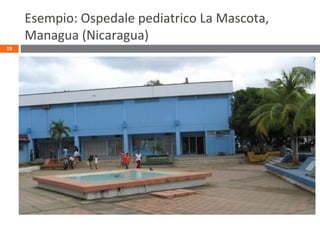
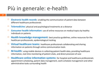
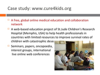
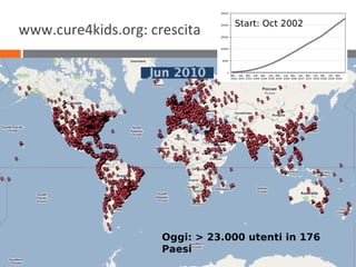

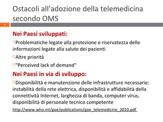
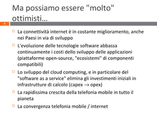
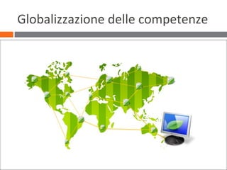
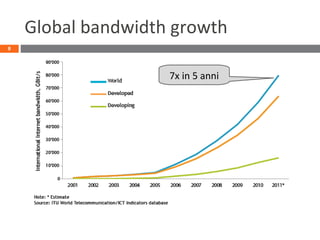
Il documento discute l'importanza della telemedicina sostenibile per i paesi in via di sviluppo, evidenziando come lo sviluppo di Internet e delle tecnologie mobili stia rendendo queste applicazioni più accessibili e a basso costo. Vengono analizzati vari tipi di specialità in telemedicina e gli ostacoli che ne ostacolano l'adozione, ma anche i segnali positivi come il miglioramento della connettività. Infine, si sottolinea il potenziale futuro della telemedicina grazie all'evoluzione tecnologica e alla globalizzazione delle competenze.


