Downloaded 352 times


![Nanoscale
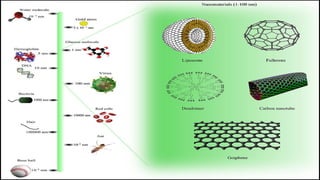
The nanoscopic scale (or nanoscale) usually refers to structures with a
length scale applicable to nanotechnology, usually cited as 1–100 nanometres.[
1] A nanometre is a billionth of a meter. The nanoscopic scale is (roughly
speaking) a lower bound to the mesoscopic scale for most solids.
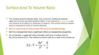
For technical purposes, the nanoscopic scale is the size at which fluctuations in
the averaged properties (due to the motion and behavior of individual
particles) begin to have a significant effect (often a few percent) on the
behavior of a system, and must be taken into account in its analysis.
The nanoscopic scale is sometimes marked as the point where the properties of
a material change; above this point, the properties of a material are caused by
'bulk' or 'volume' effects, namely which atoms are present, how they are
bonded, and in what ratios. Below this point, the properties of a material
change, and while the type of atoms present and their relative orientations are
still important, 'surface area effects' (also referred to as quantum effects)
become more apparent – these effects are due to the geometry of the material
(how thick it is, how wide it is, etc.), which, at these low dimensions, can have
a drastic effect on quantized states, and thus the properties of a material.](https://image.slidesharecdn.com/presentationonnanotechnology-141122231230-conversion-gate01/85/Presentation-on-nano-technology-5-320.jpg)


The document provides an overview of nanotechnology, defining it as the manipulation of materials at the nanoscale (1-100 nanometers) and detailing its applications in electronics, medicine, and various industries. It discusses the properties of nanomaterials, particularly carbon nanotubes, and their structural types, as well as the benefits and challenges associated with nanotechnology, including potential health risks and environmental impacts. The text emphasizes the revolutionary potential of nanotechnology while also acknowledging its considerable costs and dangers.


