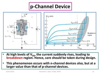
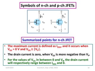
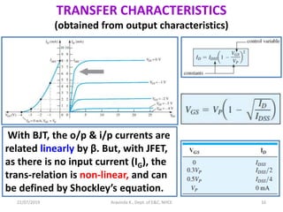
Download to read offline

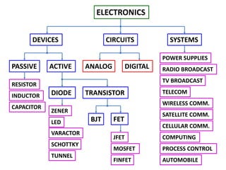
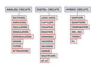
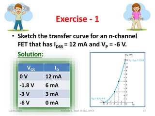


This document discusses electronics circuits and devices. It covers topics like transistors, diodes, resistors, capacitors, inductors, integrated circuits, analog circuits, digital circuits, and more. Circuit examples include rectifiers, amplifiers, oscillators, filters, logic gates, memories, microprocessors, and more. The document also discusses specific concepts related to JFET devices, including their characteristics, regions of operation, and comparisons to BJT devices. Sample problems are provided to illustrate transfer characteristics of n-channel JFETs.


![Water level indicator [autosaved]](https://cdn.slidesharecdn.com/ss_thumbnails/waterlevelindicatorautosaved-151215123305-thumbnail.jpg?width=640&height=640&fit=bounds)