Download to read offline
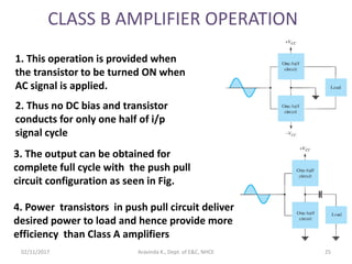
![TRANSISTOR
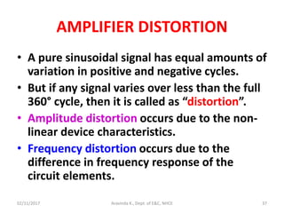
POWER RATING
• The maximum power handled by a transistor is
specified at ambient temperature.
• When the temperature exceeds the ambient one,
then in order to prevent the destruction of the
transistor, either a larger heat sink has to be used,
or the power needs to be derated.
• P2 = P1 - [(T2-T1)DF] where DF = Derating Factor.
02/11/2017 Aravinda K., Dept. of E&C, NHCE 43](https://image.slidesharecdn.com/aecmodule5-200302072725/85/Analog-Electronic-Circuits-Module-5-43-320.jpg)
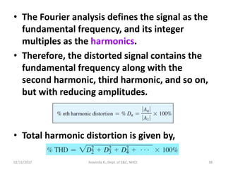
![Problem: Determine the maximum power
dissipation allowed for an 80 W Silicon transistor, if
derating is required above 25°C, by a derating factor
of 0.5 W/°C at a case temperature of 125°C.
Answer: Power at 125°C = 80-[(125-25)0.5] = 30 W.
02/11/2017 Aravinda K., Dept. of E&C, NHCE 44](https://image.slidesharecdn.com/aecmodule5-200302072725/85/Analog-Electronic-Circuits-Module-5-44-320.jpg)
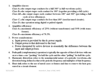


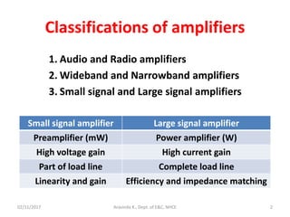
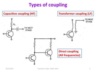
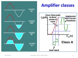
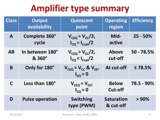
This document provides an overview of power amplifiers in analog electronic circuits. It discusses classifications of amplifiers including small signal vs large signal amplifiers. It also covers types of coupling such as capacitive, transformer, and direct coupling. The document then describes amplifier classes including classes A, B, C and D. It provides details on topics like load lines, efficiency calculations, distortion and phase splitter circuits as they relate to power amplifier design and operation. Worked examples are included throughout to illustrate key concepts.


![EE-304 Electrical Network Theory [Class Notes1] - 2013](https://cdn.slidesharecdn.com/ss_thumbnails/ee30420130802graph-130917043018-phpapp01-thumbnail.jpg?width=640&height=640&fit=bounds)


![[Back2School] STA Methodology- Chapter 7pdf](https://cdn.slidesharecdn.com/ss_thumbnails/stamethodology-250624214856-5fd24ebc-thumbnail.jpg?width=640&height=640&fit=bounds)


![RF Module Design - [Chapter 6] Power Amplifier](https://cdn.slidesharecdn.com/ss_thumbnails/rfch6-150613070347-lva1-app6891-thumbnail.jpg?width=640&height=640&fit=bounds)