Download to read offline
![Amos H Jeeva Oli, R Rani Hemamalini / International Journal of Engineering Research and
Applications (IJERA) ISSN: 2248-9622 www.ijera.com
Vol. 3, Issue 3, May-Jun 2013, pp.388-392
388 | P a g e
Part-by-Part-Evaluation-on-Arrival approach involving modified
eight point radix-2 FFT/IFFT for an OFDM transceiver to reduce
latency
Amos H Jeeva Oli1
, R Rani Hemamalini2
1
Research Scholar, St. Peter‟s University, Chennai. India
2
Professor & Head, Department of ECE, St. Peter‟s College of Engineering & Technology, Chennai, India
Abstract
An OFDM transceiver which will have
the FFT/IFFT as an integral part will suffer
latency due to the latter. This paper reduces the
latency for a OFDM transceiver involving a 512
point FFT/IFFT function by using a modified 8
point radix2 FFT/IFFT. It performs Part-by-
Part-Evaluation-on-Arrival instead of evaluating
FFT after the arrival of a full set of 512 input
samples. This approach significantly reduces the
latency in the OFDM transceiver and usage of a
modified 8 point radix 2 FFT/IFFT as the basic
unit to evaluate the large 512 point FFT/IFFT
also reduces the computational requirements.
The same has been implemented in a Spartan 3
FPGA.
Keyword: FFT, IFFT, PPEA, Symbol Combiner,
latency, OFDM transceiver
1. Introduction
FFT and IFFT functions are the central and
integral part of any OFDM system. FFT and IFFT
functions are used to multiplex low data rate signals
over orthogonal carriers to mitigate ISI which is
severe when the data rate is high in multipath
propagation environ. But the functions can be
performed only after the arrival of all the inputs. So
the FFT and IFFT is modified to accommodate Part-
by-part-evaluation-on-arrival to reduce the initial
waiting time. The FFT or IFFT functions for a large
value of N can become very complex if the PPEA
approach is applied. So the large FFT or IFFT is
performed by involving smaller FFT or IFFTs.
Among the smaller FFTs 4 point or 8 point FFTs or
IFFTs are preferred, since they use very less number
of or no twiddle factor multiplications. It should be
noted that the a 4 point FFT will involve only
complex additions while 8 point FFT will involve
only complex one multiplication.
A N2
point FFT can be realized by
decomposing it into a 2 dimensional structure of N
point FFTs [1], shift and add multiplier can be used
to avoid using a RAM or ROM, for example a
64point FFT can be realised by decomposing it into
a 2 dimensional structure of 8 point FFTs. Two
cascaded parallel/pipelined radix 4 Butterfly Unit
can form a R-16 butterfly processing element, this
facilitates low complexity realization of radix 16
butterfly operation and high operation speed.[2]
FFT processor for OFDM systems can be made
efficient by using Parallel Butterfly algorithm, for
example using a Dual Butterfly algorithm gives
high throughput and requires relatively small
areas[3]. FFT computations can be reconstructed
into a scalable array structure based on an 8 point
Butterfly Unit – the array structure can easily
expand along both the horizontal and vertical
dimensions for any point FFT computation [4].
There are applications when a non power of two
FFT would need to be performed, the corresponding
algorithm is complex, a power of two algorithms
can be used to perform it [5]. Normally zero valued
inputs outnumber the non-zero valued input in the
FFT block; there are pruning algorithms that are
available, especially dynamically partial
reconfigurable transform decompositions FFT
which is architecturally efficient for FPGA
implementation [6].
A fixed point 16 bit word width 64 point
FFT/IFFT processor, that is a OFDM based
IEEE802.11a wireless LAN baseband processor
realised by decomposing it into a 2 dimensional
structure of 8 point FFT is realised using a shift and
add multiplier without any RAM or ROM[7]. Hence
from an 8 point FFT a higher input FFT can be
easily developed. OFDM can also occur in 2 MIMO
OFDM modes namely, space frequency block coded
OFDM and space division multiplexed OFDM [8].
A frequency hopping OFDM was developed
allowing more flexibility, lower complexity, better
acquisition and synchronization performance [9]
where the FH was based on sampling rate
conversion. OFDM, FFT and symbol processing
need high frequency clock rates hence needing high
electrical power but minimizing electrical power is
more critical that the number of implemented logic
gates [10]. Demodulation of the OFDM signal can
also be performed in the discrete time signalling
domain before ADC after FFT operation, since it
significantly reduces the required number of bits in
the ADC while increasing receiver linearity [11] &
[12]. Usage of low power register files and resource
sharing techniques reduce the power consumed
[13].A flexible adaptivity of internal bit vector](https://image.slidesharecdn.com/bm33388392-130511060212-phpapp01/85/Bm33388392-1-320.jpg)
![Amos H Jeeva Oli, R Rani Hemamalini / International Journal of Engineering Research and
Applications (IJERA) ISSN: 2248-9622 www.ijera.com
Vol. 3, Issue 3, May-Jun 2013, pp.388-392
388 | P a g e
Part-by-Part-Evaluation-on-Arrival approach involving modified
eight point radix-2 FFT/IFFT for an OFDM transceiver to reduce
latency
Amos H Jeeva Oli1
, R Rani Hemamalini2
1
Research Scholar, St. Peter‟s University, Chennai. India
2
Professor & Head, Department of ECE, St. Peter‟s College of Engineering & Technology, Chennai, India
Abstract
An OFDM transceiver which will have
the FFT/IFFT as an integral part will suffer
latency due to the latter. This paper reduces the
latency for a OFDM transceiver involving a 512
point FFT/IFFT function by using a modified 8
point radix2 FFT/IFFT. It performs Part-by-
Part-Evaluation-on-Arrival instead of evaluating
FFT after the arrival of a full set of 512 input
samples. This approach significantly reduces the
latency in the OFDM transceiver and usage of a
modified 8 point radix 2 FFT/IFFT as the basic
unit to evaluate the large 512 point FFT/IFFT
also reduces the computational requirements.
The same has been implemented in a Spartan 3
FPGA.
Keyword: FFT, IFFT, PPEA, Symbol Combiner,
latency, OFDM transceiver
1. Introduction
FFT and IFFT functions are the central and
integral part of any OFDM system. FFT and IFFT
functions are used to multiplex low data rate signals
over orthogonal carriers to mitigate ISI which is
severe when the data rate is high in multipath
propagation environ. But the functions can be
performed only after the arrival of all the inputs. So
the FFT and IFFT is modified to accommodate Part-
by-part-evaluation-on-arrival to reduce the initial
waiting time. The FFT or IFFT functions for a large
value of N can become very complex if the PPEA
approach is applied. So the large FFT or IFFT is
performed by involving smaller FFT or IFFTs.
Among the smaller FFTs 4 point or 8 point FFTs or
IFFTs are preferred, since they use very less number
of or no twiddle factor multiplications. It should be
noted that the a 4 point FFT will involve only
complex additions while 8 point FFT will involve
only complex one multiplication.
A N2
point FFT can be realized by
decomposing it into a 2 dimensional structure of N
point FFTs [1], shift and add multiplier can be used
to avoid using a RAM or ROM, for example a
64point FFT can be realised by decomposing it into
a 2 dimensional structure of 8 point FFTs. Two
cascaded parallel/pipelined radix 4 Butterfly Unit
can form a R-16 butterfly processing element, this
facilitates low complexity realization of radix 16
butterfly operation and high operation speed.[2]
FFT processor for OFDM systems can be made
efficient by using Parallel Butterfly algorithm, for
example using a Dual Butterfly algorithm gives
high throughput and requires relatively small
areas[3]. FFT computations can be reconstructed
into a scalable array structure based on an 8 point
Butterfly Unit – the array structure can easily
expand along both the horizontal and vertical
dimensions for any point FFT computation [4].
There are applications when a non power of two
FFT would need to be performed, the corresponding
algorithm is complex, a power of two algorithms
can be used to perform it [5]. Normally zero valued
inputs outnumber the non-zero valued input in the
FFT block; there are pruning algorithms that are
available, especially dynamically partial
reconfigurable transform decompositions FFT
which is architecturally efficient for FPGA
implementation [6].
A fixed point 16 bit word width 64 point
FFT/IFFT processor, that is a OFDM based
IEEE802.11a wireless LAN baseband processor
realised by decomposing it into a 2 dimensional
structure of 8 point FFT is realised using a shift and
add multiplier without any RAM or ROM[7]. Hence
from an 8 point FFT a higher input FFT can be
easily developed. OFDM can also occur in 2 MIMO
OFDM modes namely, space frequency block coded
OFDM and space division multiplexed OFDM [8].
A frequency hopping OFDM was developed
allowing more flexibility, lower complexity, better
acquisition and synchronization performance [9]
where the FH was based on sampling rate
conversion. OFDM, FFT and symbol processing
need high frequency clock rates hence needing high
electrical power but minimizing electrical power is
more critical that the number of implemented logic
gates [10]. Demodulation of the OFDM signal can
also be performed in the discrete time signalling
domain before ADC after FFT operation, since it
significantly reduces the required number of bits in
the ADC while increasing receiver linearity [11] &
[12]. Usage of low power register files and resource
sharing techniques reduce the power consumed
[13].A flexible adaptivity of internal bit vector](https://image.slidesharecdn.com/bm33388392-130511060212-phpapp01/75/Bm33388392-1-2048.jpg)
![Amos H Jeeva Oli, R Rani Hemamalini / International Journal of Engineering Research and
Applications (IJERA) ISSN: 2248-9622 www.ijera.com
Vol. 3, Issue 3, May-Jun 2013, pp.388-392
389 | P a g e
widths when a IFFT/FFT is performed was analysed
[14].
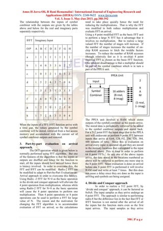
2. Symbol Combiner
Conventionally, if FFT/IFFT needs to be
performed on the incoming symbols they are
received and are either shuffled or not shuffled
depending on whether decimation is done in the
time domain or frequency domain. In this paper
decimation in the time domain is preferred, hence
incoming symbols are operated upon and 8 different
real and imaginary outputs are generated & stored
only to be retrieved after a given time delay to be
added with the 8 real and imaginary outputs
generated then. The real and imaginary values
which are accumulated at 8 different equi-spaced
instants of time are normally stored and retrieved in
& from a memory with negligible retrieval and re-
storage time. The tables given below define how
symbol combiner operates on a given input symbol.
If the input to the symbol combiner of a FFT
function at a given instant of time is given by xr+jxi,
then the 8 outputs of the symbol combiner will be
xr:(0), xi:(1), -xr:(2), -xi:(3), 0.707*(xr+xi):(4),
0.707*(xr-xi):(5), -0.707(xr+xi):(6) and -0.707(xr-
xi):(7). If the inputs are denoted as a, b, c, d, e, f, g
and h and the outputs as A, B, C, D, E, F and H the
below table describes how every input goes to the
symbol combiner and produces values that are
routed to the corresponding output, that is which
output of the symbol combiner is assigned and
accumulated location, both for real and imaginary.
FFT Real Input
O/P a b c d e f g h
A 0 0 0 0 0 0 0 0
B 0 4 1 7 2 6 3 5
C 0 1 2 3 0 1 2 3
D 0 7 3 4 2 5 1 6
E 0 2 0 2 0 2 0 2
F 0 6 1 5 2 4 3 7
G 0 3 2 1 0 3 2 1
H 0 5 3 6 2 7 1 4
FFT Imaginary Input
O/P a b c d e f g h
A 1 1 1 1 1 1 1 1
B 1 7 2 6 3 5 0 4
C 1 2 3 0 1 2 3 0
D 1 6 0 7 3 4 2 5
E 1 3 1 3 1 3 1 3
F 1 5 2 4 3 7 0 6
G 1 0 3 2 1 0 3 2
H 1 4 0 5 3 6 2 7
Similarly the inputs for a IFFT function is given by
A, B, C, D, E, F and H and the outputs by a, b, c, d,
e, f, g and h.
IFFT Real Input
O/P A B C D E F G H
a 0 0 0 0 0 0 0 0
b 0 5 3 6 2 7 1 4
c 0 3 2 1 0 3 2 1
d 0 6 1 5 2 4 3 7
e 0 2 0 2 0 2 0 2
f 0 7 3 4 2 5 1 6
g 0 1 2 3 0 1 2 3
h 0 4 1 7 2 6 3 5](https://image.slidesharecdn.com/bm33388392-130511060212-phpapp01/85/Bm33388392-2-320.jpg)
![Amos H Jeeva Oli, R Rani Hemamalini / International Journal of Engineering Research and
Applications (IJERA) ISSN: 2248-9622 www.ijera.com
Vol. 3, Issue 3, May-Jun 2013, pp.388-392
391 | P a g e
undergo 8 point FFT operations, but the 8 points
they correspond with will be 64 (512/8) input
samples away, hence the symbol combining is
performed and the results are stored temporarily to
be retrieved and added to the symbol combiner
outputs at the instants of arrival of consecutive
inputs samples that are 64 samples away.
0 1 2 … 511
0 8 16 …. 504
1 9 17 …. 505
2 10 18 …. 506
3 11 19 …. 507
4 12 20 …. 508
5 13 21 …. 509
6 14 22 ….. 510
7 15 23 …. 511
0 64 128 … 448
8 72 136 … 456
16 80 144 … 464
24 88 152 … 472
32 96 160 … 480
40 104 168 … 488
48 112 176 … 496
56 120 184 … 504
1 65 129 … 449
9 73 137 … 457
17 81 145 … 465
25 89 153 …. 473
33 97 161 … 481
41 105 169 … 489
49 113 177 … 497
57 121 185 … 505
.
.
.
7 71 135 … 455
15 79 143 …. 463
23 87 151 ….. 471
31 95 159 ….. 479
39 103 167 ….. 487
47 111 175 ….. 495
55 119 183 ….. 503
63 127 191 ….. 511
The above tables clearly show that a 512 point FFT
is first divided to form eight 64 point FFTs. Every
64 point FFT can be further divided into eight 8
point FFTs. A eight point FFT will have to be
performed row wise in a 8 x 8 matrix, followed by
multiplication of every element in the matrix by
WN
r1c1
, where N=8 and r1=0 to 7 and c1=0 to 7.
This is in turn followed by performing a column
wise 8 point FFT. This, though it appears like any
„divide and conquer‟ approach is done with the help
of the modified 8 point radix 2 FFT, hence can be
performed as and when the final entries in the 8
locations of interest is made. This in turn will
reduce the latency in waiting for a stage to complete
and a partial PPEA is being used.
When this 3 step procedure of performing
8 row wise 8 point FFTs, followed by multiplication
by twiddle factors and 8 column wise 8 point FFTs
is completed a 64 point FFT has been performed.
When this 3 step procedure is repeated eight 64
point FFT are performed. The results of these FFTs
are stored in a 64 x 8 matrix for further
manipulation. Conversion of eight 64 point FFTs in
a 512 point FFT can be done with a help of a 2 step
procedure namely, multiplying every entry in the 8 x
64 matrix is multiplied by a twiddle factor WN
r1c1
,
where N=64 and r1=0 to 7 and c1=0 to 63 and
following it by eight column wise 8 point FFTs. In
the 3 step procedure to evaluate the 64 point FFTs
and 2 step procedure to convert eight 64 point FFTs
into 512 point FFT wherever 8 point FFTs are
performed it is done with the help of the PPEA unit.
5. Conclusion
The 512 point FFT/IFFT using the PPEA
unit was realized in a Xilinx Spartan 3 FPGA. The
usage of the smaller-sized eight-point FFTs for
calculating the large 512-point FFT reduced the
complexity of the FFT/IFFT function. The usage of
the Part-by-Part-Evaluation-on-Arrival approach
reduced the difference between time of arrival of the
last of the input samples and the time at which the
first output is calculated. This reduces the latency in
the calculation of FFT/IFFT. This reduction in
computational complexity and latency is evidenced
in the device utilization details and the timing
summary observed during synthesis based on the
Spartan 3 target device chosen.
References
[1] Koushik Maharatna, Eckhard Grass, Ulrich
Jagdhold, A 64 point Fourier Transform
Chip for High speed Wireless Lan
Application using OFDM IEEE Journal of
Solid State Circuits, Vol.39, No.3
[2] Shen Jui Huang, Sau Gee Chen A High
throughput Radix-16 FFT processor with
parallel and Normal input/output ordering
for IEEE 802.15.3c (WPANS) systems
IEEE transactions on Circuits and systems
I: regular papers
[3] Haining Jiang, Hanwen Luo, Jifeng Tian
and Wentao Song, Design of an efficient
FFT processor for OFDM systems IEEE
transactions on consumer electronics, Vol.
51, No. 4
[4] Xuan Guan, Yunsi Fei, Hai Lin
Hierarchical Design of an Application-
Specific Instruction Set Processor for High-
Throughput and Scalable FFT Processing](https://image.slidesharecdn.com/bm33388392-130511060212-phpapp01/85/Bm33388392-4-320.jpg)
![Amos H Jeeva Oli, R Rani Hemamalini / International Journal of Engineering Research and
Applications (IJERA) ISSN: 2248-9622 www.ijera.com
Vol. 3, Issue 3, May-Jun 2013, pp.388-392
392 | P a g e
IEEE Transactions on Very Large Scale
Integration (VLSI) Systems
[5] Le Jin, Lin Liang, A power-of-two FFT
algorithm and structure for DRM receiver
IEEE transactions on Consumer
Electronics
[6] Vennila C; Palaniappan C T K; Krishna K
V; Lakshminarayanan G; Seok Bum Ko,
Dynamic partial reconfigurable FFT/IFFT
pruning for OFDM based Cognitive radio,
IEEE International Symposium on Circuits
and Systems
[7] “A 64 point Fourier Transform Chip for
High speed Wireless Lan Application using
OFDM”, Koushik Maharatna, Eckhard
Grass, Ulrich Jagdhold, IEEE Journal of
Solid State Circuits, Vol.39, No.3, March
2004
[8] “Design and Implementation of MIMO
OFDM Baseband processor for High Speed
Wireless LANS” Yunho Jung, Jiho kim,
Seongjoo Lee, Hongil Yoon, Jaeseok Kim,
IEEE transactions on Circuits and Systems-
II: Express Briefs, Vol 54. No. 7, July 2007
[9] “All digital baseband frequency hopping
OFDM system”, Qicun Shi, Zhixing Yang,
Lifeng He, Kewu Peng, IEEE Singapore
International Conference on
Communication systems, June 2008
[10] “A Double data rate Architecture for
OFDM based Wireless Consumer devices”,
R. Simon Sheratt, Oswaldo Cadenas, IEEE
Transactions on Consumer Electronics,
Vol. 56, No. 1, February 2010
[11] “A Discrete-time FFT processor for UWB
OFDM wireless transceivers: Architecture
and Behavioural Modelling”, Mark Lehne,
Sanjay Raman, IEEE transactions on
Circuits and Systems –I: regular papers.
Vol 57, No.11, November 2010
[12] “A 0.13 um 1GS/s CMOS DT FFT
processor for UWB OFDM wireless
receivers, Mark Lehne, Sanjay Raman”,
IEEE transactions on Microwave Theory
and Techniques. Vol. 59, no.6, June 2011
[13] “Design and Implementation of a Low-
Power OFDM receiver for Wireless
Communications” Chu Yu, Chen-Hen
Sung, Chien Hung Kuo, Mao Hsu Yen,
Sao-Jie Chen IEEE Transactions on
Consumer Electronics, August 2012
[14] Dreschmann M; Meyer J; Hubner
M;SchmogrowR; Hillerkuss D; Becker J;
Leuthold J; Freude W, Implementation of
an ultra high speed 256 point FFT for
Xilinx Virtex 6 devices, IEEE conference
on Industrial Informatics
Authors’ Information
Amos H Jeeva Oli is a research scholar of St. Peter‟s
University, who completed Bachelor‟s in
Electronics and Communication Engineering in
1995 and Masters in Microwave and Optical
Engineering in 2003. He is currently working in R
M D Engineering College as Associate
Professor/ECE. He has published papers in refereed
International journals.
R Rani Hemamalini, is Professor and Head of
Electronics and Communication Engineering
department in St. Peter‟s College of Engineering
and Technology. She completed Bachelors in
Electrical and Electronics Engineering in 1990,
Masters in Process Controls in 1997 and
Instrumentation and Doctorate in Control
Engineering in 2003. She has published over 30
papers in refereed International journals, involved in
research in foreign universities. She has been
involved in sponsored research over the last 10
years.](https://image.slidesharecdn.com/bm33388392-130511060212-phpapp01/85/Bm33388392-5-320.jpg)

The paper presents a method for reducing latency in an OFDM transceiver by implementing a modified 8-point radix-2 FFT/IFFT approach that allows part-by-part evaluation upon the arrival of input samples. This technique minimizes the waiting time for input data to accrue before computation starts, dramatically enhancing performance while also lowering computational requirements. The proposed method has been implemented in a Spartan 3 FPGA, highlighting its practical application for efficient OFDM signal processing.


![Getting Started with Apache Spark: Big Data Made Simple [Free Meetup]](https://cdn.slidesharecdn.com/ss_thumbnails/apachesparkgettingstarted-260203175547-8361bcc3-thumbnail.jpg?width=640&height=640&fit=bounds)


