The document describes the design of reversible comparators and decoders using a novel 4x4 reversible gate called the inventive gate. It introduces the inventive gate and shows how it can realize various logic functions like AND, OR, XOR, etc. It then presents the design of a 2-to-4 reversible decoder using the inventive gate that generates 2 garbage outputs and requires 4 gates. Lemmas are provided to show an n-to-2n reversible decoder can be designed using a minimum of 2n+1 gates. The document goes on to describe the design of 1-bit, 2-bit, 8-bit, 32-bit and n-bit reversible comparators using the inventive gate with low values for
![International Journal of VLSI design & Communication Systems (VLSICS) Vol.5, No.5, October 2014
EVOLUTION OF STRUCTURE OF SOME BINARY
GROUP-BASED N-BIT COMPARATOR, N-TO-2N
DECODER BY REVERSIBLE TECHNIQUE
Neeraj Kumar Misra1
, Subodh Wairya2
and Vinod Kumar Singh3
Department of Electronics Engineering,
Institute of Engineering and Technology, Lucknow, India
ABSTRACT
Reversible logic has attracted substantial interest due to its low power consumption which is the main
concern of low power VLSI circuit design. In this paper, a novel 4x4 reversible gate called inventive
gate has been introduced and using this gate 1-bit, 2-bit, 8-bit, 32-bit and n-bit group-based reversible
comparator have been constructed with low value of reversible parameters. The MOS transistor
realizations of 1-bit, 2- bit, and 8-bit of reversible comparator are also presented and finding power,
delay and power delay product (PDP) with appropriate aspect ratio W/L. Novel inventive gate has the
ability to use as an n-to-2n
decoder. Different proposed novel reversible circuit design style is
compared with the existing ones. The relative results shows that the novel reversible gate wide utility,
group-based reversible comparator outperforms the present design style in terms of number of gates,
garbage outputs and constant input.
KEYWORDS
Reversible Logic, Inventive Gate, Garbage Output, Constant input, Full subtraction, n-bit reversible
comparator, Reversible decoder etc.
1.INTRODUCTION
In low power VLSI circuit, planning of power is one of important aspects. According to
Landauer [1] in 1960 demonstrate that single bit of information loss generate at least KT ln2 J/K
of energy where K is the Boltzmann constant (1.38x10⁻²³
J/K) and T is the absolute temperature.
Reversible circuits are totally different from irreversible circuits. In reversible logic no bits is loss
the circuit that doesn't loss information is reversible.
C.H Bennet [2] in 1973 proves that KT ln2 joule of energy wouldn't be dissipated if the
reversible circuit consist of reversible gates only. Thus reversible logic operations do not loss
information and dissipate less heat also as power. Thus reversible logic is probably going to be
in demand in high speed power aware circuits. A reversible circuit planning has following
important attributes such as Garbage output, number of reversible gates, constant inputs, all
should be minimum for efficient reversible circuits.
Comparator has wide applications in Analog and digital circuits, Analog to digital (A/D)
converters, Level shifter, and communication system etc. It compares the 2-number of several
DOI : 10.5121/vlsic.2014.5502 9](https://image.slidesharecdn.com/vlsicscomparator-150725200600-lva1-app6891/85/EVOLUTION-OF-STRUCTURE-OF-SOME-BINARY-GROUP-BASED-N-BIT-COMPARATOR-N-TO-2N-DECODER-BY-REVERSIBLE-TECHNIQUE-1-320.jpg)
![International Journal of VLSI design & Communication Systems (VLSICS) Vol.5, No.5, October 2014
EVOLUTION OF STRUCTURE OF SOME BINARY
GROUP-BASED N-BIT COMPARATOR, N-TO-2N
DECODER BY REVERSIBLE TECHNIQUE
Neeraj Kumar Misra1
, Subodh Wairya2
and Vinod Kumar Singh3
Department of Electronics Engineering,
Institute of Engineering and Technology, Lucknow, India
ABSTRACT
Reversible logic has attracted substantial interest due to its low power consumption which is the main
concern of low power VLSI circuit design. In this paper, a novel 4x4 reversible gate called inventive
gate has been introduced and using this gate 1-bit, 2-bit, 8-bit, 32-bit and n-bit group-based reversible
comparator have been constructed with low value of reversible parameters. The MOS transistor
realizations of 1-bit, 2- bit, and 8-bit of reversible comparator are also presented and finding power,
delay and power delay product (PDP) with appropriate aspect ratio W/L. Novel inventive gate has the
ability to use as an n-to-2n
decoder. Different proposed novel reversible circuit design style is
compared with the existing ones. The relative results shows that the novel reversible gate wide utility,
group-based reversible comparator outperforms the present design style in terms of number of gates,
garbage outputs and constant input.
KEYWORDS
Reversible Logic, Inventive Gate, Garbage Output, Constant input, Full subtraction, n-bit reversible
comparator, Reversible decoder etc.
1.INTRODUCTION
In low power VLSI circuit, planning of power is one of important aspects. According to
Landauer [1] in 1960 demonstrate that single bit of information loss generate at least KT ln2 J/K
of energy where K is the Boltzmann constant (1.38x10⁻²³
J/K) and T is the absolute temperature.
Reversible circuits are totally different from irreversible circuits. In reversible logic no bits is loss
the circuit that doesn't loss information is reversible.
C.H Bennet [2] in 1973 proves that KT ln2 joule of energy wouldn't be dissipated if the
reversible circuit consist of reversible gates only. Thus reversible logic operations do not loss
information and dissipate less heat also as power. Thus reversible logic is probably going to be
in demand in high speed power aware circuits. A reversible circuit planning has following
important attributes such as Garbage output, number of reversible gates, constant inputs, all
should be minimum for efficient reversible circuits.
Comparator has wide applications in Analog and digital circuits, Analog to digital (A/D)
converters, Level shifter, and communication system etc. It compares the 2-number of several
DOI : 10.5121/vlsic.2014.5502 9](https://image.slidesharecdn.com/vlsicscomparator-150725200600-lva1-app6891/75/EVOLUTION-OF-STRUCTURE-OF-SOME-BINARY-GROUP-BASED-N-BIT-COMPARATOR-N-TO-2N-DECODER-BY-REVERSIBLE-TECHNIQUE-1-2048.jpg)
![International Journal of VLSI design & Communication Systems (VLSICS) Vol.5, No.5, October 2014
2
bits. In this paper introduce group-based n-bit reversible comparator [6,9,11] and n-to-2n
reversible decoder with low value of reversible parameters with the help of various lemmas.
This paper is organized with the following sections: Section 2 and 3 discuss basic definition
of reversible logic; Section 4 discuss the past work; Section 5 discuss the utility and design
issue of novel 4x4 inventive gate; Section 6 Planning of low value style reversible comparator
subsection of 6.1 introduce novel 1-bit comparator cell, subsection 6.2 and 6.3 is novel match,
larger and smaller comparator cell design; Subsection 6.4, 6.5, 6.6 and 6.7 for 2-bit, 8-bit, 32-
bit and n- bit group-based reversible comparator design respectively; Section 7 Implement
all comparator cell in MOS transistor with minimum MOS transistor count. Section 8 categories
as simulation result of comparator. Finally, the paper is concluded and future work with Section
9.
2. BASIC DEFINITIONS OF REVERSIBLE LOGIC
In this section, we introduce the essential definitions of reversible logic which are relevant with
this research work.
Definition 2.1 A reversible gate is a Z - input and Z - output that generate a unique output pattern
for each possible input pattern.
Definition 2.2 In Reversible logic output and input is equal in number. And unwanted output is
called garbage output it should be minimum as possible.
3.PARAMETER OPTIMIZED FOR DESIGNING EFFICIENT REVERSIBLE
CIRCUITS
The main challenge of designing efficient reversible circuits is to optimize the different reversible
parameters which result the circuit design is costly. The most necessary parameters which have
dominant in efficient reversible logic circuits are:
3.1 Garbage output
Unutilized or unwanted output of reversible circuit is called garbage output. It should be kept
minimum as possible.
3.2 Constant Input
Constant bits are additional inputs that are not part of the original specification. These bits are
added in hopes to reduce the circuit complexity or realize a reversible function. They come in the
form of a constant logic 1 or 0. It is ideal to keep in minimal.
3.3 Few Reversible gates utilized
In this subsection, we present few reversible gates that are used to design for planning different
types of reversible circuit. First TR (3×3) utilize input (A, B, C) and carry output (P=A,
Q= BA , C'ABR , Second BME gate(4X4) utilize input (A, B, C, D) and carry output](https://image.slidesharecdn.com/vlsicscomparator-150725200600-lva1-app6891/85/EVOLUTION-OF-STRUCTURE-OF-SOME-BINARY-GROUP-BASED-N-BIT-COMPARATOR-N-TO-2N-DECODER-BY-REVERSIBLE-TECHNIQUE-2-320.jpg)
![International Journal of VLSI design & Communication Systems (VLSICS) Vol.5, No.5, October 2014
3
(P=A, CABQ , CADR ) and DCB'AS , Third Feynman gate (FG) 2x2
utilize input (A, B ) and carry output (P=A, BAR ), Fourth Peres gate (PG) 3x3 utilize
input (A, B, C) and carry output (P=A, , BAQ , CABR )
3.4 Flexibility
Flexibility refers to the universality of reversible logic gate in realizing more logical function.
4. PAST WORK
In 2010, Himanshu thapliyal et.al [17] design a reversible 8-bit and 64-bit tree-based comparator
using TR Gate that has the latency of O(log2(n)).But this approach is not suitable for low value
of reversible parameter and not extended for n-bit reversible comparator. Furthermore another
comparator design by Rangaraju et.al., [7, 8] in 2011 has shown that design has input circuit as
first stage and 1-Bit comparator cell as second stage and so on. This idea is extend for n-bit
reversible comparator design but it is not sufficient to optimizing the reversible parameter. In
2011, Nagamani et.al. [21] Design a reversible 1-bit reversible comparator with low value of
reversible parameter but this idea is not extended for n-bit comparator.
In 2013, Ri-gui Zhou et.al. [5] design a novel 4-bit reversible comparator. It is mentioned in
paper further possibilities of reducing the number of reversible gates, constant input and garbage
output in the area of reversible comparator design. They proposed new gate and using this gate
form various gate AND, OR, XNOR, NOT, FA, FS but not form gate NAND, NOR. For
increasing order of comparator, gate increase in higher order and complexity of design increases
and also garbage outputs means performance of comparator degrade.
In 2013, Hafiz Md. Hasan babu et.al. [4] design compact n-bit reversible comparator. Its design is
efficient because it reduce complexity of design. Approach is sufficient and proposed various
theorem and lemma for calculating n-bit reversible parameter number of gate, total delay, power.
They proposed two new gate BJS and HLN. These gate form OR, AND, XOR and NOT
Operation but not form FA, FS, NAND and NOR Operation. For showing expertise of reversible
gate we work on this and proposed Universal gate called Inventive Gate. It’s performing all
logical operation NAND, NOR, AND, OR, HA, HS, FA and FS and also form efficient group-
based n-bit reversible comparator and n-to-2n
bit decoder with low value of reversible parameters.
5. UTILITY AND DESIGN ISSUES OF FRESHLY PROJECTED 4X4
INVENTIVE GATE
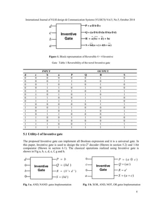
In this section, a new 4 x 4 reversible gate named as Inventive gate, is proposed. The
block representation of inventive gate is depicted in Figure 1. The corresponding truth table
drawn in Table 1. The inventive gate generates 4 outputs that are defined as follows
cbaP , )da(bc)dba(Q , bca)dcb(R and )cab(d)ca(dbS
of inventive gate.](https://image.slidesharecdn.com/vlsicscomparator-150725200600-lva1-app6891/85/EVOLUTION-OF-STRUCTURE-OF-SOME-BINARY-GROUP-BASED-N-BIT-COMPARATOR-N-TO-2N-DECODER-BY-REVERSIBLE-TECHNIQUE-3-320.jpg)
![International Journal of VLSI design & Communication Systems (VLSICS) Vol.5, No.5, October 2014
5
Inventive
Gate
a
0
c
1
''caS
Inventive
Gate bcR
1
b
c
d cbP
dbS
Fig.1 c. NOR gate Implementation Fig. 1 d. XNOR, AND gates Implementation
a
0
b
0 )( baP
abQ
1
baQInventive
Gate
a
0
b
)( baP
Inventive
Gate
Fig. 1 e. Half adder Implementation Fig. 1 f. Half subtraction Implementation.
a
c
b
0
a
0
b
0
Inventive
Gate
Inventive
Gate
cbaP
abc)ba(Q
cbaP
bac)ba(Q
Fig. 1 g. Full adder Implementation Fig. 1 h. Full subtraction Implementation
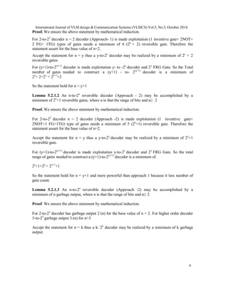
5.2. Utility-2 of Reversible inventive gate as reversible n-to-2n
decoder
In this section we show the utility-2 of Inventive gate. It performs the operation of Reversible 2-
to-22
decoder it consists of two approaches named as approach - 1 and approach - 2. Approach- 1
of 2-to-22
decoder generate 2 garbage output and number of gate count is 5. Whereas the
Approach - 2 generate 2 garbage output but reduces number of gate count is 4 as shown in
Figure 2 (b). And also implement of 3-to-23
decoder (Approach 2) generate 3 garbage output
and number of gate count 7 as shown in Figure 4. Decoder [3, 11, 14] are widely used in
applications like information multiplexing, 7 segment show and memory addressing.
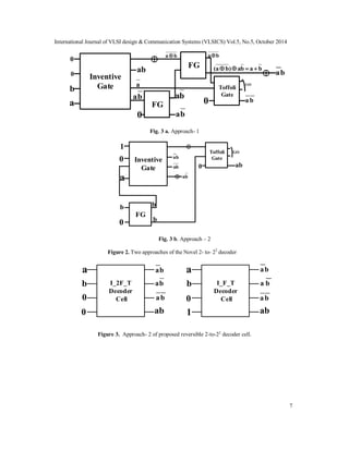
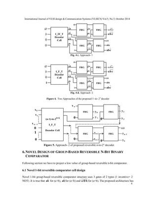
5.2.1 Reversible 2-to-22
decoder and 3-to-23
decoder
Planning of Reversible 2-to-22
decoder is shown in Figure 2(b). It consists of (1 inventive gate+
2NOT+ 1 FG+ 1TG) types of gates. It has two input marked a, b apply to inventive gate and
Feynman gate (FG) respectively obtained output is passed to TG and gives output is (ab) other
output of decoder is (a' b), (a b') and (a' b'). Completed cell of 2-to-22
decoder are named as
I_F_T decoder cell. These cell are utilize for designing 3-to-23
decoder as shown in Figure 4.
Lemma 5.2.1.1 An n-to-2n
reversible decoder (Approach 1) may be accomplished by a minimum
of 2n
+ 2 reversible gates, where n is that the range of bits and n ≥ 2](https://image.slidesharecdn.com/vlsicscomparator-150725200600-lva1-app6891/85/EVOLUTION-OF-STRUCTURE-OF-SOME-BINARY-GROUP-BASED-N-BIT-COMPARATOR-N-TO-2N-DECODER-BY-REVERSIBLE-TECHNIQUE-5-320.jpg)


![International Journal of VLSI design & Communication Systems (VLSICS) Vol.5, No.5, October 2014
15
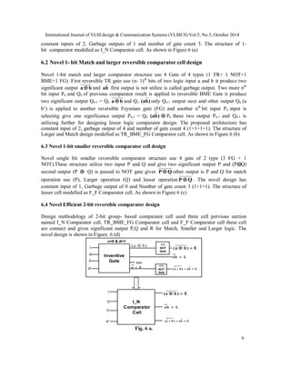
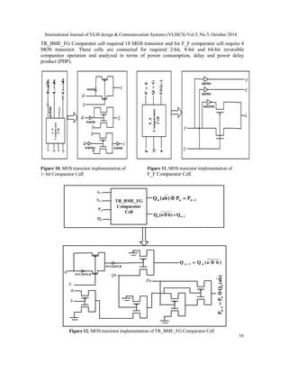
Algorithm- 2 Reversible group-based n-bit comparator
*Design a n-bit reversible binary comparator when (n ≥ 2) with minimum number of gates and
garbage output.
Begin
Step 1. Pick up I_N comparator cell and pick input Xn and output Yn for two n-bit number
1 . Xn[1] = an //nth
input of an
2. Xn[2] = bn //nth
input of bn
3. Xn[3] = 0
4. Xn[4] = 1
5. If Xn[1] < Xn[2] then
Yn[2] = Ryn=1
6. Else if Xn[1] > Xn[2] then
Yn[4] = Qyn=1
7. Else Yn[1] = Pyn = 1
End if
Step 2. For TR_BME_FG and F_F Comparator cell, Level of input and output are considered
to be Yn and Yn-1 respectively
Loop
8. For j = n - 1 to 1
Pick up TR_BME_FG Comparator cell WJ
If j = n-1 then
WJ[1] = Xn[4] = QYn
WJ[2] = Xn[1] = PYn
WJ[3] = bn-1
WJ[4] = an-1
Else
WJ[1] = WJ-1[2] = QYn-1
WJ[2] = WJ-1[1] = PYn-1
WJ[3] = aj //(n-1)th
input of an
WJ[4] = bj //(n-1)th
input of bn
End if
End loop
9. Step 3. Pick up F_F Comparator cell and pick input V and output Z
V[1]= W[1]
V[2] = W[2]
V[3] = 0
Z[1] = W[1]
Z[2] = [W[1] W[2]] 1
Z[3] = W[2]
10. End
7. MOS TRANSISTOR IMPLEMENTATION OF DIFFERENT
COMPARATOR CELL
In this section implement different comparator cell in MOS transistor with minimum MOS
transistor count. MOS transistor implementations of 2-bit comparator uses 14 MOS transistors,](https://image.slidesharecdn.com/vlsicscomparator-150725200600-lva1-app6891/85/EVOLUTION-OF-STRUCTURE-OF-SOME-BINARY-GROUP-BASED-N-BIT-COMPARATOR-N-TO-2N-DECODER-BY-REVERSIBLE-TECHNIQUE-15-320.jpg)

![International Journal of VLSI design & Communication Systems (VLSICS) Vol.5, No.5, October 2014
19
1
x 10
-12
0.8
0.6
0.4
0.2
0
0.7 0.8 0.9 1 1.1 1.2 1.3 1.4 1.5
InputVoltage(V)
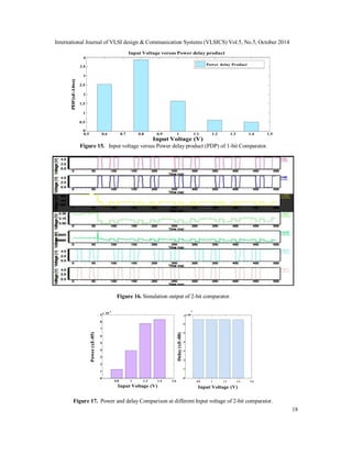
Figure 18. Input voltage versus Power delay product (PDP) of 2-bit Comparator.
Maximum Power and Delay Variation(s) versus Channel Length Variation(u)
1 2 4 6 8
Channel Length Variation (nm)
Figure 19. Channel Length Variation versus power and delay of 2-bit Comparator
Table 2. Comparison between anticipated and existing in terms of expertise of reversible gate
RGate Gate can be used as n-
bit comparator
Single Gate can be
used as Full
subtractor
Gate can be
used as n-to-2n
decoder
Anticipated Inventive
Gate
Y Y Y
Available Circuit [4] Y N N
Available Circuit [3] N N Y
Available Circuit [12] N N N
Available Circuit [13] N N N
Available Circuit [15] N N N
Available Circuit [6] Y N N
Available Circuit [5] Y Y N
Maximum Power variation (xE-05)
Maximum Delay variation (xE-08)
10
8
6
4
2
PDP(xE-13)](https://image.slidesharecdn.com/vlsicscomparator-150725200600-lva1-app6891/85/EVOLUTION-OF-STRUCTURE-OF-SOME-BINARY-GROUP-BASED-N-BIT-COMPARATOR-N-TO-2N-DECODER-BY-REVERSIBLE-TECHNIQUE-19-320.jpg)
![International Journal of VLSI design & Communication Systems (VLSICS) Vol.5, No.5, October 2014
20
Table 3. Comparison between anticipated and existing style comparator in terms of NOG, GO, CI, power
and delay
Methods NOG GO CI Power (µW) Delay (ns)
Anticipated work 6+4(n-1) 1+4(n-1) 1+2n (85.81n – 78.98) (115.010n – 100.854)
Thaplial et al.
[17] 9n (6n −6) -- (268.23n −239.2) {0.23 x log2(n) + 0.1}
Vudadha et al.
[18] (4n −2) (5n −4) -- (122.36n −60.36) {0.09*log2(n) + 0.2}
Rangaraju et al.
[7 ] (7n −4) (5n −4) -- (182.53n +76.55) (0.2n − 0.16)
Hafiz Md. Hasan
Babu [ 4] 3n (4n-3) 3 (117.76n −32.94) (0.15n − 0.03)
NOG-number of gate, GO-Garbage output, CI-Constant input, Y=Yes, N=No
Table 4 Comparison between anticipated and existing style Comparator in terms of garbage output and
constant input](https://image.slidesharecdn.com/vlsicscomparator-150725200600-lva1-app6891/85/EVOLUTION-OF-STRUCTURE-OF-SOME-BINARY-GROUP-BASED-N-BIT-COMPARATOR-N-TO-2N-DECODER-BY-REVERSIBLE-TECHNIQUE-20-320.jpg)
![International Journal of VLSI design & Communication Systems (VLSICS) Vol.5, No.5, October 2014
21
9. CONCLUSION AND FUTURE WORK
This paper is mainly focused on novel design of the reversible 4x4 inventive Gate. It utilized as
1-bit, 2-bit, 8-bit, 32-bit and n-bit group-based binary comparator and n-to-2n
decoder. Moreover,
the low value styles of reversible parameter have been established for the proposed circuits. For
example, and n-to-2n
decoder uses at least 2n
+ 1 reversible gates and its n garbage output: an n-
bit comparator utilize 6+4 (n - 1) number of reversible gate, 1+4 (n-1) garbage output. The
proposed group- based comparator achieves the improvement of 19.87% in terms of garbage
output and 31.57% in terms of constant input over the existing one [7]. Simulation of the novel
comparator circuits have shown that it works correctly and finding parameter power and delay.
The proposed circuits will be useful for implementing the ALU and control unit of processor.
ACKNOWLEDGMENT
Authors would like to acknowledge Research Cum Teaching Fellowship through TEQIP-II
provide by World Bank for the financial support for this work.
REFERENCES
[1] J R.Landauer, “Irreversibility and Heat Generation in the Computational Process”, IBM Journal of
Research and Development, pp: 183-191, 1961.
[2] C H Bennett, “Logical Reversibility of Computation,” IBM Journal of Research and Development,
vol. 17, no. 6, pp. 525-532, November 1973.
[3] Lafifa Jamal, Md. Masbaul Alam, Hafiz Md. Hasan Babu, “An efficient approach to design a
reversible control unit of a processor” Elsevier Sustainable Computing: Informatics and Systems pp:
286-294, 2013
[4] Hafiz Md. Hasan Babu, Nazir Saleheen, Lafifa Jamal, Sheikh Muhammad Sarwar,Tsutomu Sasao
"Approach to design a compact reversible low power binary comparator" IET Computers & Digital
Techniques" Vol. 8, Iss. 3, pp. 129–139 doi: 10.1049/iet-cdt.2013.0066, 2014
[5] Ri-gui Zhou, Man-qun Zhang, QianWu •Yan-cheng Li "Optimization Approaches for Designing a
Novel 4-Bit Reversible Comparator" Springer International jounal of theoretical physics DOI
10.1007/s10773-012-1360-ypp:559-575, 2013
[6] Farah Sharmin, Rajib Kumar Mitra, Rashida Hasan, Anisur Rahman "Low cost reversible signed
comparator" International Journal of VLSI design & Communication Systems” Vol.4, No.5,pp:19-
33,2013
[7] Rangaraju H G, Vinayak Hegdeb, Raja K B, Muralidhara K N "Design of Efficient Reversible Binary
Comparator" Elsevier International Conference on Communication Technology and System Design
Procedia Engineering pp:897-904, 2012
[8] Rangaraju, H.G., Hegde, V., Raja, K.B., Muralidhara, K.N. “Design of low power reversible binary
comparator”. Proc. Engineering (ScienceDirect), 2011
[9] Bahram Dehghan, Abdolreza Roozbeh, Jafar Zare "Design of Low Power Comparator Using DG
Gate" Scientific research ciruits and systems doi.org/10.4236/cs.2013.51002pp: 7-12, 2014
[10] Pallavi Mall, A.G.Rao, H.P.Shukla "Novel Design of Four-Bit Reversible Numerical Comparator"
International Journal of Advanced Research in Computer and Communication Engineering Vol. 2,
Issue 4 pp: 1808-1807, 2013
[11] Neeta Pandey, Nalin Dadhich, Mohd. Zubair Talha "Realization of 2-to-4 reversible decoder and its
applications" International Conference on Signal Processing and Integrated Networks (SPIN) pp: 349-
353,2014
[12] Md. M. H Azad Khan, “Design of Full-adder With Reversible Gates”, International Conference on
Computer and Information Technology, Dhaka, Bangladesh, 2002, pp. 515-519](https://image.slidesharecdn.com/vlsicscomparator-150725200600-lva1-app6891/85/EVOLUTION-OF-STRUCTURE-OF-SOME-BINARY-GROUP-BASED-N-BIT-COMPARATOR-N-TO-2N-DECODER-BY-REVERSIBLE-TECHNIQUE-21-320.jpg)
![International Journal of VLSI design & Communication Systems (VLSICS) Vol.5, No.5, October 2014
30
[13] Hafiz Md. Hasan Babu, Md. Rafiqul Islam, Syed Mostahed Ali Chowdhury and Ahsan Raja
Chowdhury ,“Reversible Logic Synthesis for Minimization of Full Adder Circuit”, Proceedings of the
EuroMicro Symposium on Digital System Design(DSD’03), 3-5 September 2003,
[14] Neeraj Kumar Misra, Subodh Wairya, Vinod Kumar Singh “Preternatural Low-Power Reversible
Decoder Design in 90 nm Technology Node” International Journal of Scientific & Engineering
Research, Volume 5, Issue 6, pp: 969-978, June 2014
[15] J.W. Bruce, M.A. Thornton,L. Shivakumariah, P.S. Kokate and X.Li, "Efficient Adder Circuits Based
on a Conservative Logic Gate", Proceedings of the IEEE Computer Society Annual Symposium on
VLSI(ISVLSI'02),April 2002, Pittsburgh, PA, USA, pp 83-88.
[16] Lafifa Jamal, Md. Masbaul Alam Polash "On the Compact Designs of Low Power Reversible
Decoders and Sequential Circuits" Springer LNCS7373, pp. 281–288, 2012.
[17] Himanshu Thapliyal, Nagarajan Ranganathan and Ryan Ferreira "Design of a Comparator Tree Based
on Reversible Logic" 10th IEEE International Conference on Nanotechnology Joint Symposium with
Nano Korea pp:1113-1116, 2010
[18] Vudadha, C.Phaneendra, P.S.,Sreehari,V.Ahmed,S.E.Muthukrishnan, N.M.Srinivas “Design of
prefix-based Optimal reversible comparator” IEEE Computer Society Annual Symp. On VLSI pp.
201–206
[19] Nagamani, A.N., Jayashree, H.V., Bhagyalakshmi, H.R.: ‘Novel low power comparator design using
reversible logic gates’, Indian J. Comput. Sci. Eng.vol 2, (4), pp. 566–574, 2011
[20] Morrison, M., Lewandowski, M., Ranganathan “Design of a tree-based comparator and memory unit
based on a novel reversible logic structure” IEEE Computer Society Annual Symp. on VLSI, pp.
331–336, 2012
[21] Neeraj Kumar Misra, Subodh Wairya, Vinod Kumar Singh “An Inventive Design of 4*4 Bit
Reversible NS Gate” IEEE International Conference on Recent Advances and Innovation in
Engineering (ICRAIE-2014), pp: 1-6, 2014 doi no. 10.1109/ICRAIE.2014.6909323](https://image.slidesharecdn.com/vlsicscomparator-150725200600-lva1-app6891/85/EVOLUTION-OF-STRUCTURE-OF-SOME-BINARY-GROUP-BASED-N-BIT-COMPARATOR-N-TO-2N-DECODER-BY-REVERSIBLE-TECHNIQUE-22-320.jpg)


![[Deck] What's New in Spark-Iceberg Integration via DSV2.pptx](https://cdn.slidesharecdn.com/ss_thumbnails/deckwhatsnewinspark-icebergintegrationviadsv2-260210005337-25955b12-thumbnail.jpg?width=640&height=640&fit=bounds)


