Download to read offline


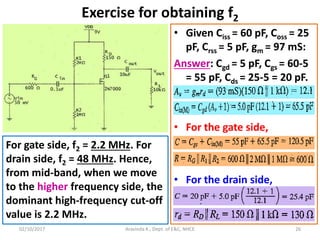
![• By utilizing the data provided by the manufacturer,
the internal capacitances can be written as –
Cgd = Crss, Cgs = Ciss – Crss and Cds = Coss – Crss
• Using Cgd, the input and output Miller capacitances
can be written as –
Cin(M) = Cgd (Av+1) and Cout(M) = Cgd [(Av+1)/Av]
• The voltage gain for the common source amplifier is
given by –
Av = gm rd where rd = RD || RL
Aravinda K., Dept. of E&C, NHCE 2502/10/2017](https://image.slidesharecdn.com/aecmodule3-200302072614/85/Analog-Electronic-Circuits-Module-3-25-320.jpg)

This document provides an overview of frequency response and analysis for amplifiers. It discusses: - How the voltage gain of an amplifier decreases at low and high frequencies due to external and internal capacitances. - Key terms like cutoff frequencies (f1 and f2), midband, and roll-off factor. - Methods for analyzing the frequency response of BJT and JFET amplifier stages to determine dominant capacitances and calculate cutoff frequencies. - Examples are provided to demonstrate the analysis process. The document covers frequency response fundamentals and analysis techniques for characterizing amplifier performance over a range of frequencies.