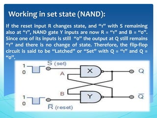
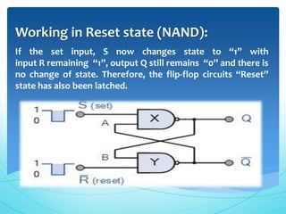
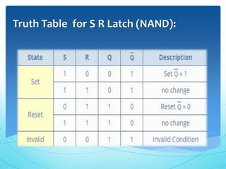
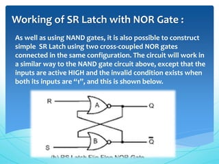
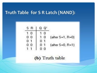
SR - Latch
To _ Sir Saleem Choudary
By _ M.Anas Awan
Syed Noman Ali
Minhaj University Lahore
Definition :
 SR latch is a circuit with two cross-coupled NOR gates
or two cross-coupled NAND gates In electronics.
 It consist of two inputs named S for Set and R for
Reset.
 It has two useful states , when output Q=1 and Q’=0 ,
and latch is said to be in Set State. When Q=0 and
Q’=1 , it is in Reset Sate.
Working in set state (NAND):
If the input (R = 0) and input (S = 1), the NAND gate Y has at
least one of its inputs 0 therefore, its output Q must be “1”
(NAND Gate principles). Output Q is also fed back to input “A”
and so both inputs to NAND gate X are “1”, and therefore its
output Q must “0”.
Working in set state (NAND):
If the reset input R changes state, and “1” with S remaining
also at “1”, NAND gate Y inputs are now R = “1” and B = “0”.
Since one of its inputs is still “0” the output at Q still remains
“1” and there is no change of state. Therefore, the flip-flop
circuit is said to be “Latched” or “Set” with Q = “1” and Q =
“0”.
Working in Reset state (NAND):
In this second stable state, Q is at logic level “0”, (not Q =
“0”) its inverse output at Q is “1”, (Q = “1”), and is given
by R = “1” and S = “0”. As gate X has one of its inputs “0” its
output Q must “1” (again NAND gate principles). Output Q is
fed back to input “B”, so both inputs to NAND gate Y are at
“1”, therefore, Q = “0”.
Working in Reset state (NAND):
If the set input, S now changes state to “1” with
input R remaining “1”, output Q still remains “0” and there is
no change of state. Therefore, the flip-flop circuits “Reset”
state has also been latched.
Truth Table for S R Latch (NAND):
Working of SR Latch with NOR Gate :
As well as using NAND gates, it is also possible to construct
simple SR Latch using two cross-coupled NOR gates
connected in the same configuration. The circuit will work in
a similar way to the NAND gate circuit above, except that the
inputs are active HIGH and the invalid condition exists when
both its inputs are “1”, and this is shown below.
Truth Table for S R Latch (NAND):
Sr Latch or Flip Flop

Sr Latch or Flip Flop

  • 1.
    SR - Latch To_ Sir Saleem Choudary By _ M.Anas Awan Syed Noman Ali Minhaj University Lahore
  • 2.
    Definition :  SRlatch is a circuit with two cross-coupled NOR gates or two cross-coupled NAND gates In electronics.  It consist of two inputs named S for Set and R for Reset.  It has two useful states , when output Q=1 and Q’=0 , and latch is said to be in Set State. When Q=0 and Q’=1 , it is in Reset Sate.
  • 3.
    Working in setstate (NAND): If the input (R = 0) and input (S = 1), the NAND gate Y has at least one of its inputs 0 therefore, its output Q must be “1” (NAND Gate principles). Output Q is also fed back to input “A” and so both inputs to NAND gate X are “1”, and therefore its output Q must “0”.
  • 4.
    Working in setstate (NAND): If the reset input R changes state, and “1” with S remaining also at “1”, NAND gate Y inputs are now R = “1” and B = “0”. Since one of its inputs is still “0” the output at Q still remains “1” and there is no change of state. Therefore, the flip-flop circuit is said to be “Latched” or “Set” with Q = “1” and Q = “0”.
  • 5.
    Working in Resetstate (NAND): In this second stable state, Q is at logic level “0”, (not Q = “0”) its inverse output at Q is “1”, (Q = “1”), and is given by R = “1” and S = “0”. As gate X has one of its inputs “0” its output Q must “1” (again NAND gate principles). Output Q is fed back to input “B”, so both inputs to NAND gate Y are at “1”, therefore, Q = “0”.
  • 6.
    Working in Resetstate (NAND): If the set input, S now changes state to “1” with input R remaining “1”, output Q still remains “0” and there is no change of state. Therefore, the flip-flop circuits “Reset” state has also been latched.
  • 7.
    Truth Table forS R Latch (NAND):
  • 8.
    Working of SRLatch with NOR Gate : As well as using NAND gates, it is also possible to construct simple SR Latch using two cross-coupled NOR gates connected in the same configuration. The circuit will work in a similar way to the NAND gate circuit above, except that the inputs are active HIGH and the invalid condition exists when both its inputs are “1”, and this is shown below.
  • 9.
    Truth Table forS R Latch (NAND):