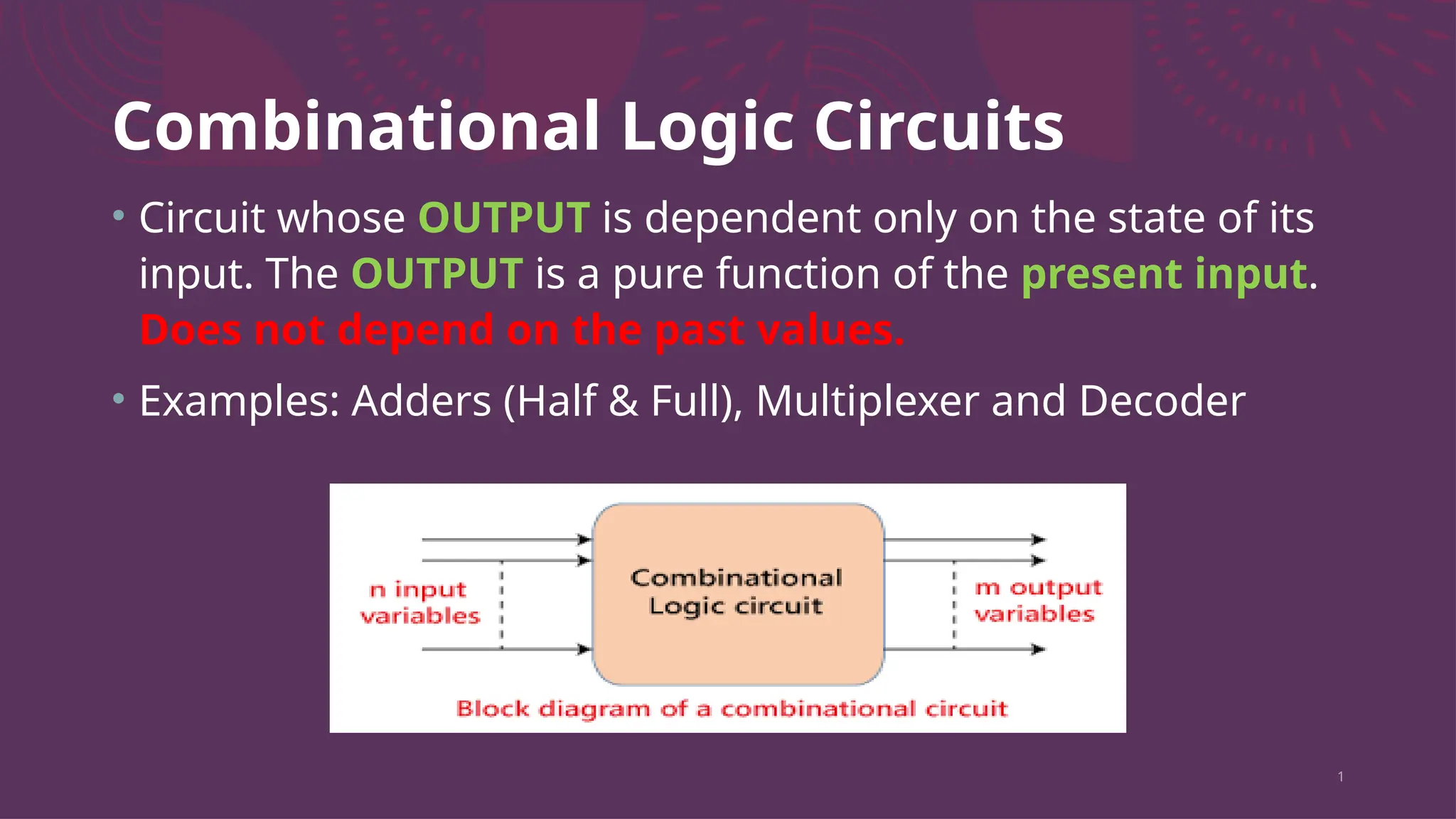
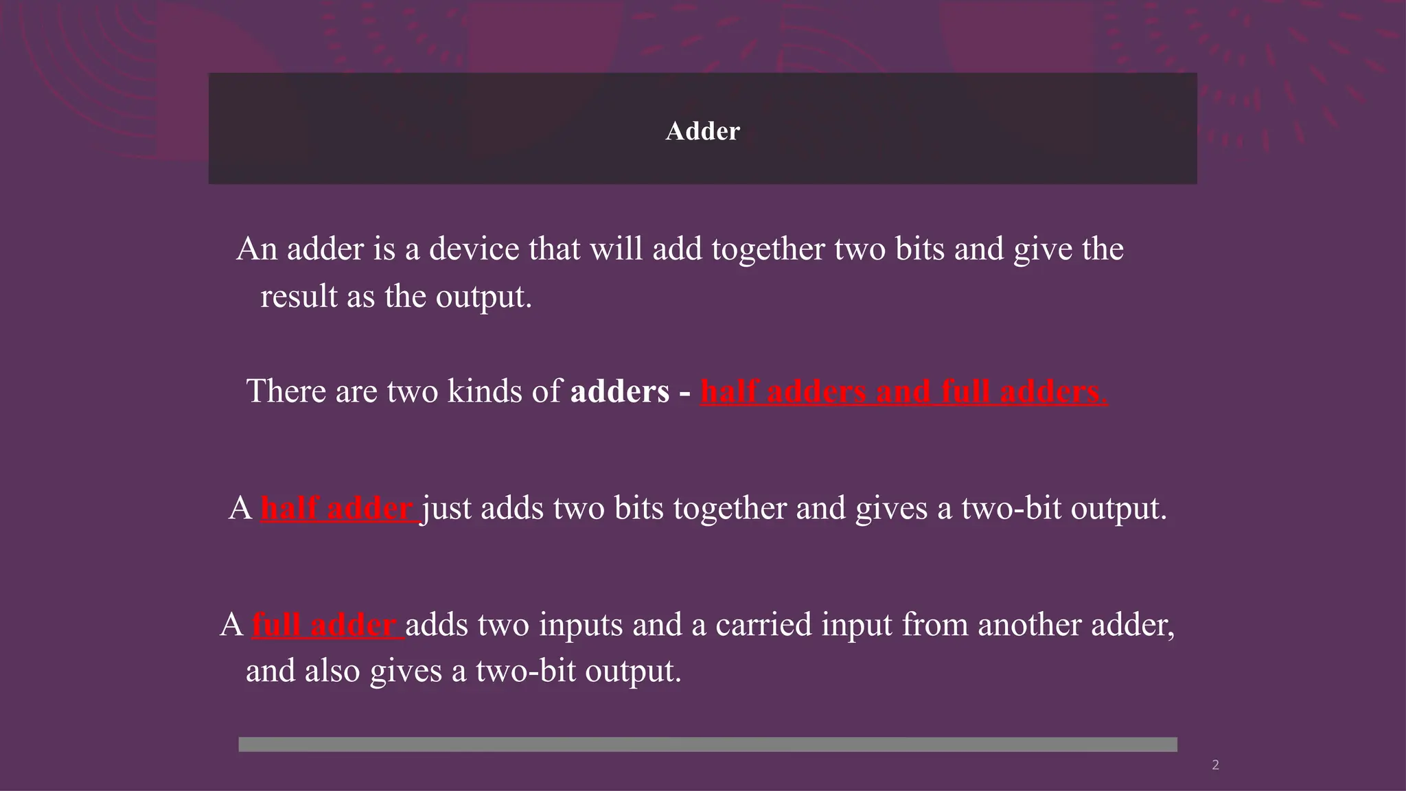
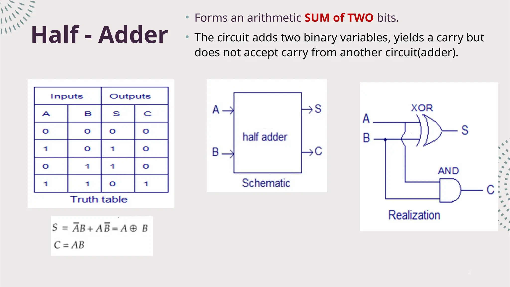
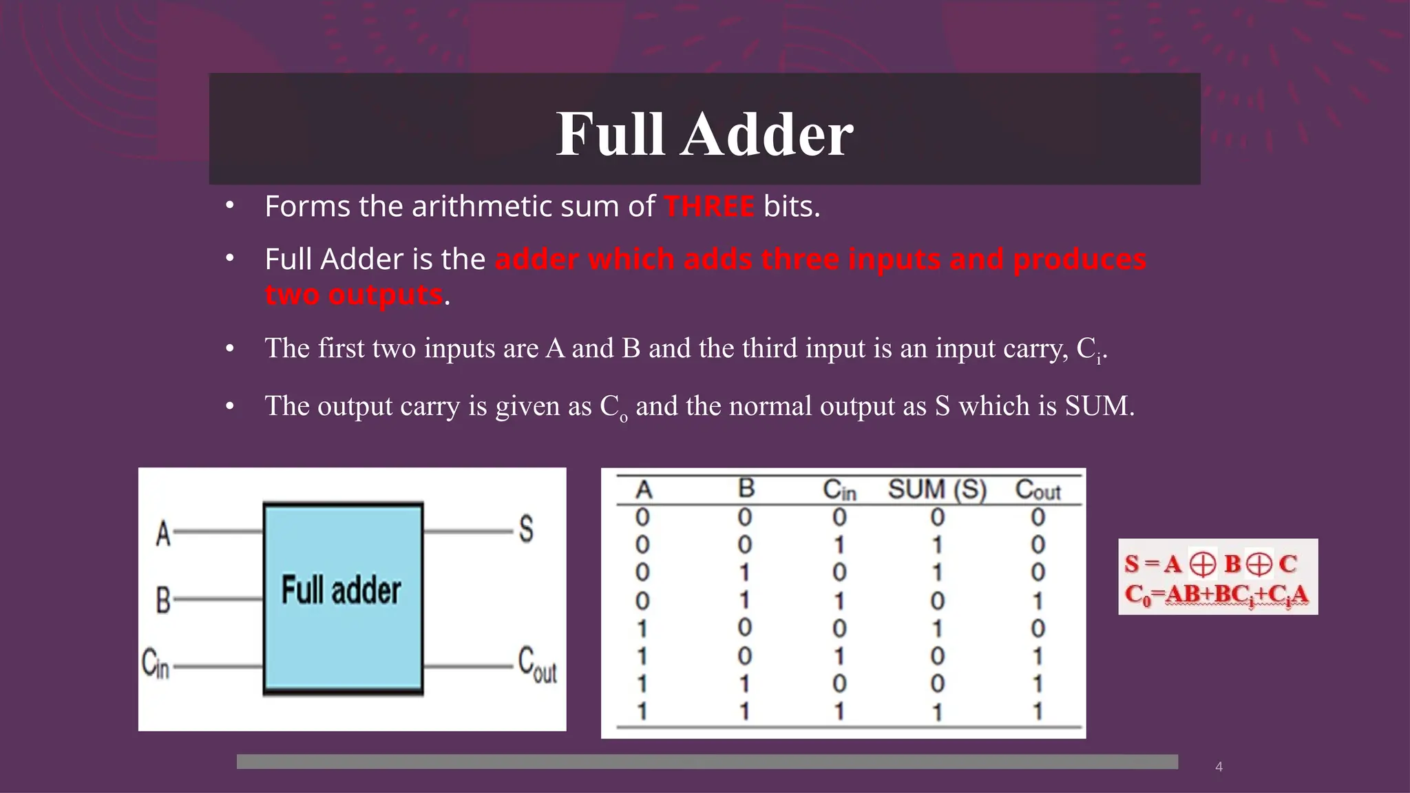
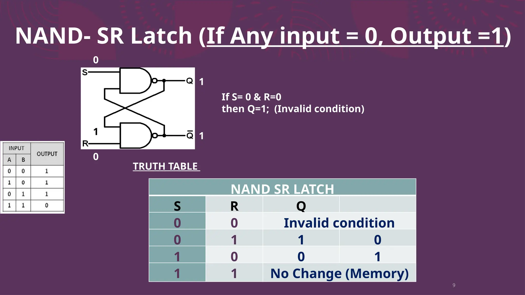
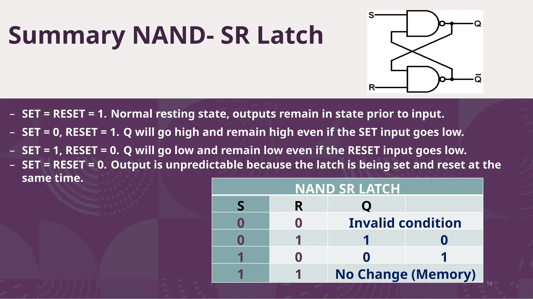
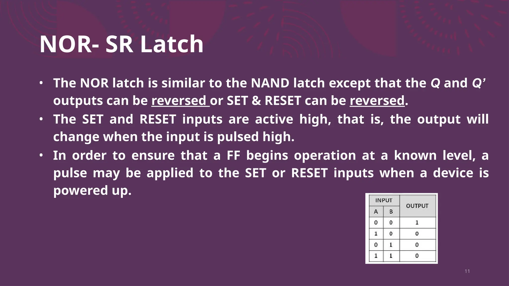
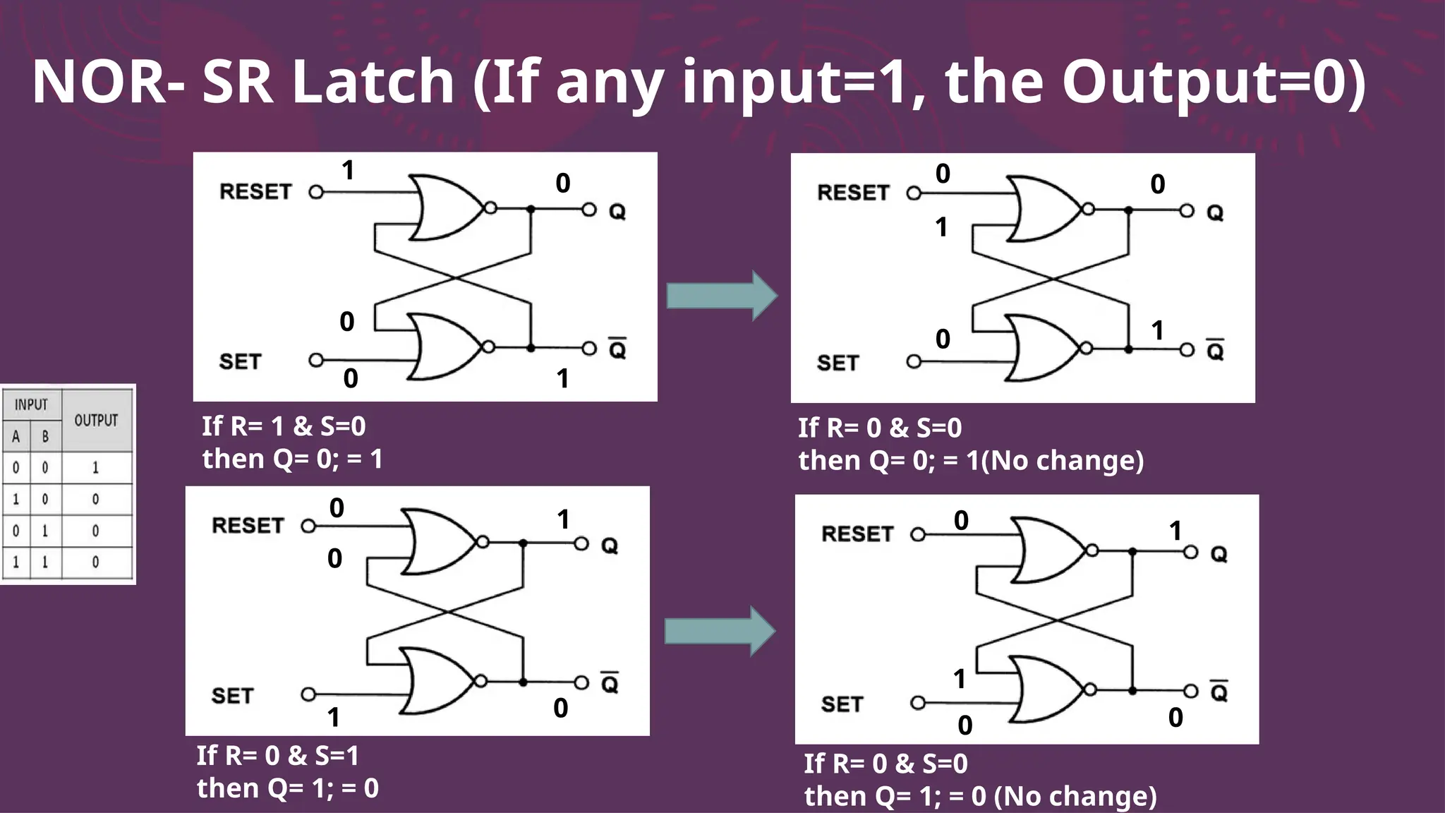
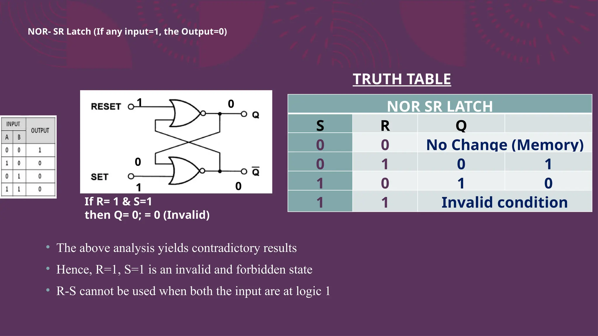
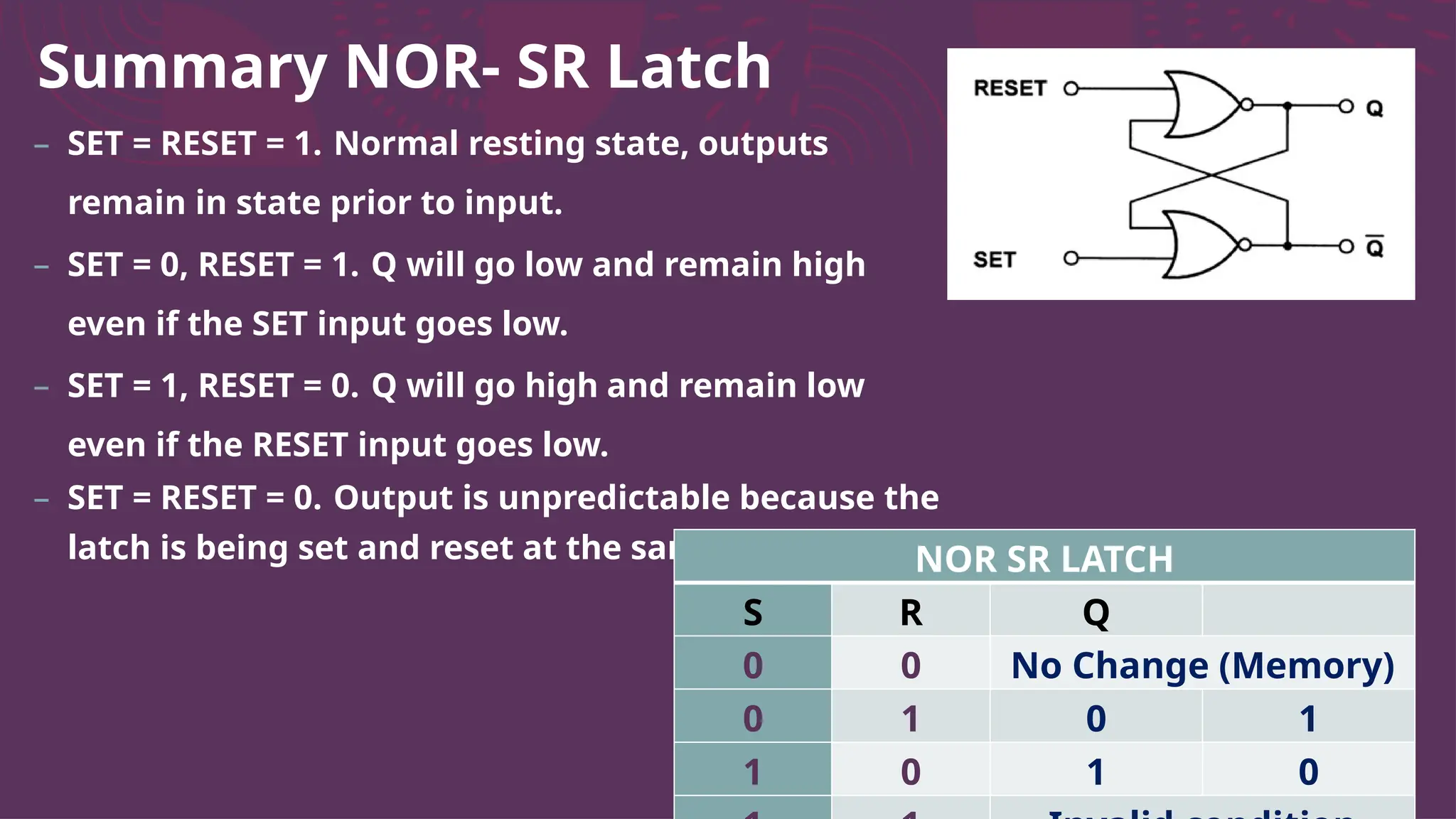
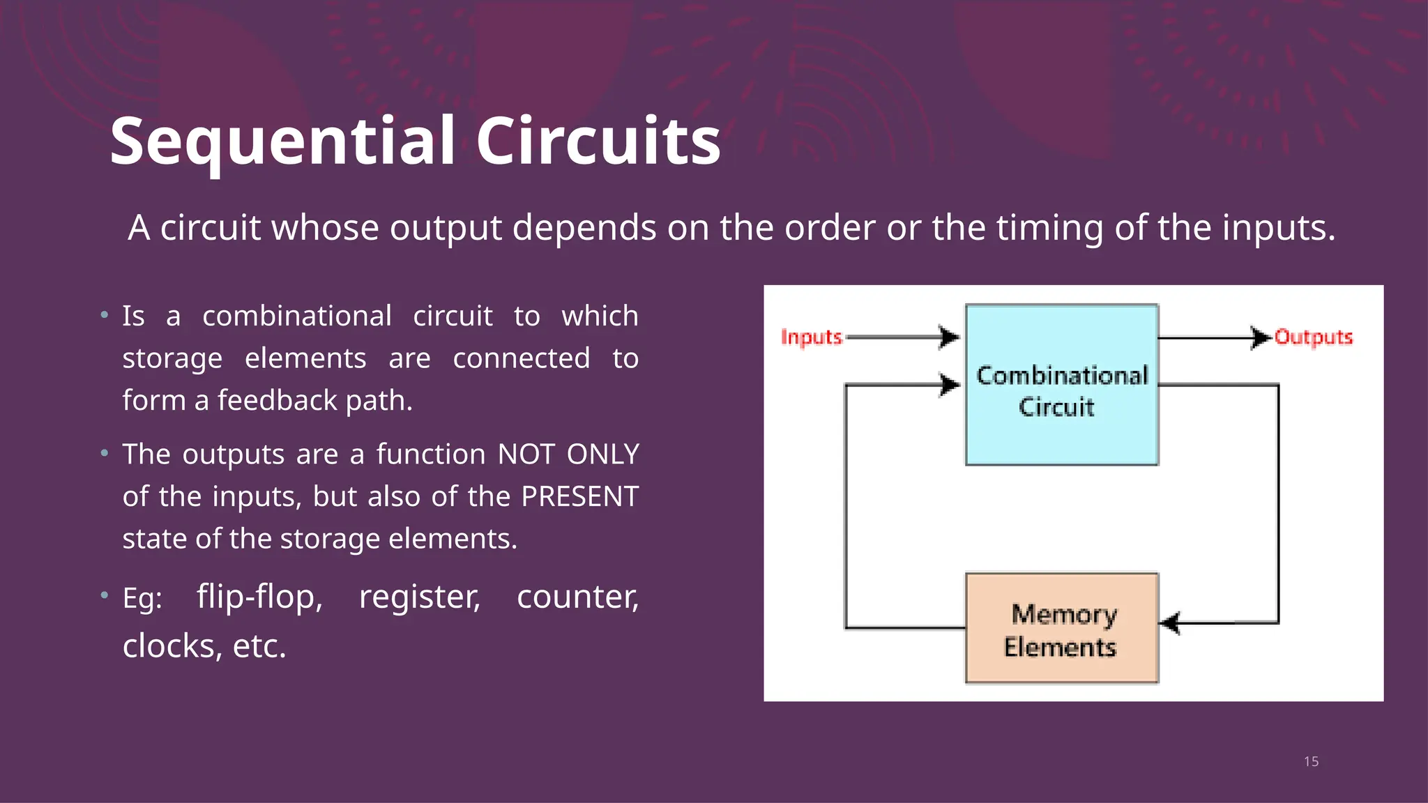
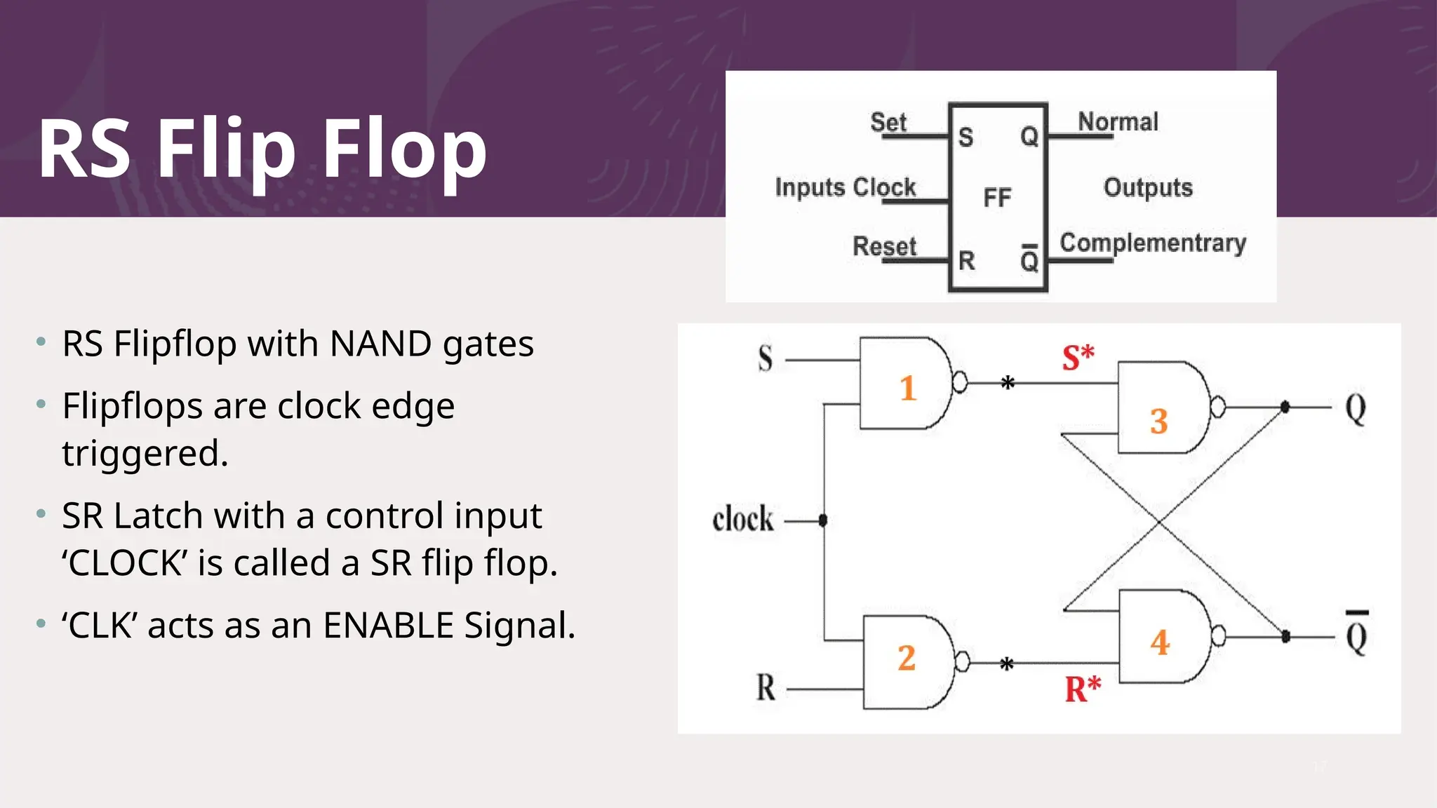
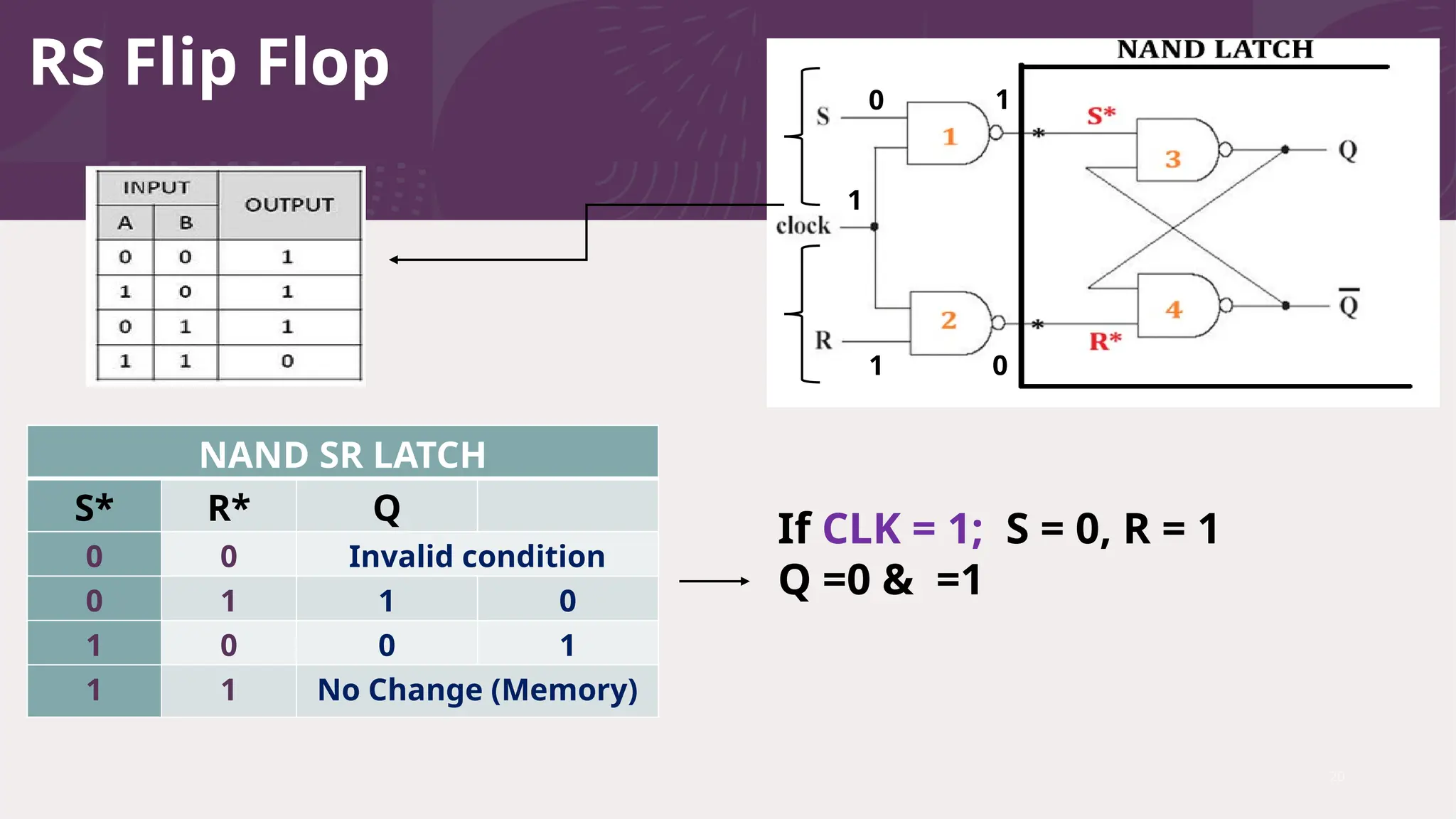
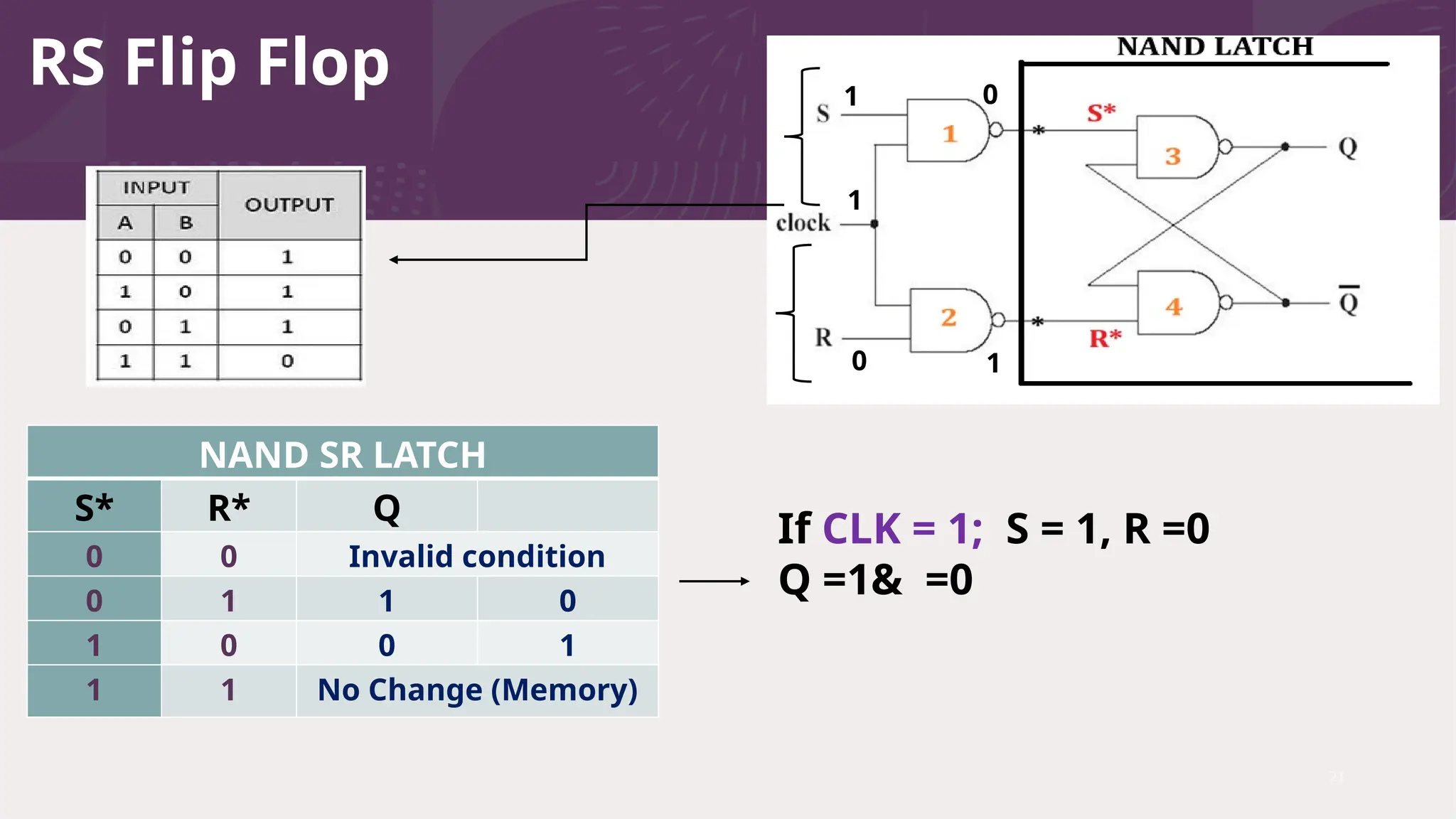
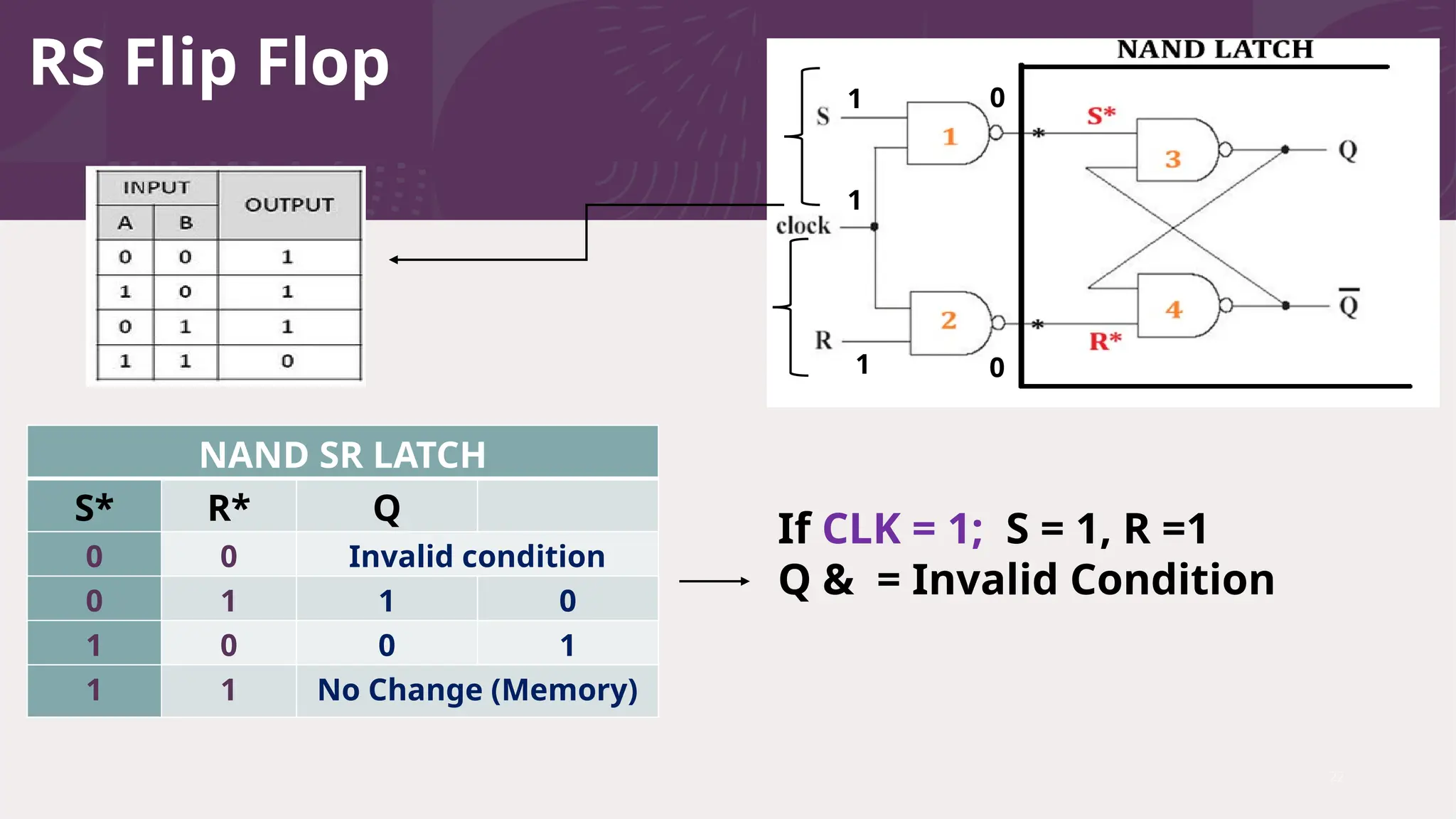
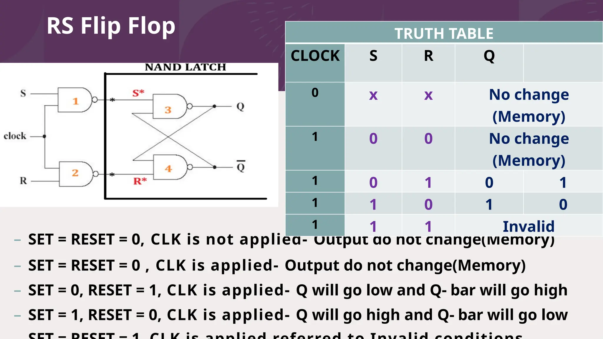
Combinational Logic Circuits
• Circuit whose OUTPUT is dependent only on the state of its
input. The OUTPUT is a pure function of the present input.
Does not depend on the past values.
• Examples: Adders (Half & Full), Multiplexer and Decoder
1
Adder
An adder is a device that will add together two bits and give the
result as the output.
There are two kinds of adders - half adders and full adders.
A half adder just adds two bits together and gives a two-bit output.
A full adder adds two inputs and a carried input from another adder,
and also gives a two-bit output.
2
Half - Adder
• Forms an arithmetic SUM of TWO bits.
• The circuit adds two binary variables, yields a carry but
does not accept carry from another circuit(adder).
3
Full Adder
4
• Forms the arithmetic sum of THREE bits.
• Full Adder is the adder which adds three inputs and produces
two outputs.
• The first two inputs are A and B and the third input is an input carry, Ci.
• The output carry is given as Co and the normal output as S which is SUM.
Full - Adder
5
It is observed from the truth table that C0=1 for rows which
have two 1’s otherwise it is 0.
Its Boolean Function is
S = A B C
C0=AB+BCi+CiA
It can be implemented by three AND and one OR gates. S=1
for rows with one 1 and three 1’s., i.e odd number of 1’s. its
implemented by a three input XOR.
6
LATCH:
• Latches are constructed from Logic gates
• Memory element
• Stores ‘1’ bit of data
• No clock
NAND – SR Latch
7
• The NAND gate latch or simply latch is a basic FF.
• The inputs are set and clear (reset) and complementary
outputs Q and
• The inputs are active low, that is, the output will
change when the input is pulsed low.
8
NAND- SR Latch (If Any input = 0, Output =1)
0
1
0
1
1
If S= 1 & R=0
then Q= 0; = 1
If S= 1 & R=1
then Q= 0; = 1(No change)
1
1
1
0
0
0
1
1
1 0
If S= 0 & R=1
then Q=1; = 0
If S= 1 & R=1
then Q=1; = 0 (No change)
1
1
1
0
0
9
NAND- SR Latch (If Any input = 0, Output =1)
0
0
1
1
If S= 0 & R=0
then Q=1; (Invalid condition)
1
TRUTH TABLE
NAND SR LATCH
S R Q
0 0 Invalid condition
0 1 1 0
1 0 0 1
1 1 No Change (Memory)
Summary NAND- SR Latch
10
– SET = RESET = 1. Normal resting state, outputs remain in state prior to input.
– SET = 0, RESET = 1. Q will go high and remain high even if the SET input goes low.
– SET = 1, RESET = 0. Q will go low and remain low even if the RESET input goes low.
– SET = RESET = 0. Output is unpredictable because the latch is being set and reset at the
same time.
NAND SR LATCH
S R Q
0 0 Invalid condition
0 1 1 0
1 0 0 1
1 1 No Change (Memory)
NOR- SR Latch
11
• The NOR latch is similar to the NAND latch except that the Q and Q’
outputs can be reversed or SET & RESET can be reversed.
• The SET and RESET inputs are active high, that is, the output will
change when the input is pulsed high.
• In order to ensure that a FF begins operation at a known level, a
pulse may be applied to the SET or RESET inputs when a device is
powered up.
NOR- SR Latch (If any input=1, the Output=0)
1
0
0
1
0
0
0
1
0
1
1
0
0
0
1
0
If R= 1 & S=0
then Q= 0; = 1
If R= 0 & S=0
then Q= 0; = 1(No change)
If R= 0 & S=1
then Q= 1; = 0
If R= 0 & S=0
then Q= 1; = 0 (No change)
0
1
0
1
NOR- SR Latch (If any input=1, the Output=0)
• The above analysis yields contradictory results
• Hence, R=1, S=1 is an invalid and forbidden state
• R-S cannot be used when both the input are at logic 1
1
1
0
0
TRUTH TABLE
If R= 1 & S=1
then Q= 0; = 0 (Invalid)
0
NOR SR LATCH
S R Q
0 0 No Change (Memory)
0 1 0 1
1 0 1 0
1 1 Invalid condition
Summary NOR- SR Latch
– SET = RESET = 1. Normal resting state, outputs
remain in state prior to input.
– SET = 0, RESET = 1. Q will go low and remain high
even if the SET input goes low.
– SET = 1, RESET = 0. Q will go high and remain low
even if the RESET input goes low.
– SET = RESET = 0. Output is unpredictable because the
latch is being set and reset at the same time. NOR SR LATCH
S R Q
0 0 No Change (Memory)
0 1 0 1
1 0 1 0
Sequential Circuits
• Is a combinational circuit to which
storage elements are connected to
form a feedback path.
• The outputs are a function NOT ONLY
of the inputs, but also of the PRESENT
state of the storage elements.
• Eg: flip-flop, register, counter,
clocks, etc.
15
A circuit whose output depends on the order or the timing of the inputs.
16
FLIPFLOP:
• Are always clocked.
• Constructed from latches from along with
an additional clock signal.
• Slow compared to Latches.
RS Flip Flop
• RS Flipflop with NAND gates
• Flipflops are clock edge
triggered.
• SR Latch with a control input
‘CLOCK’ is called a SR flip flop.
• ‘CLK’ acts as an ENABLE Signal.
17
RS Flip Flop
18
NAND SR LATCH
S* R* Q
0 0 Invalid condition
0 1 1 0
1 0 0 1
1 1 No Change (Memory)
0
1
1
If CLK = 0; S = X, R = X
Q & = No Change(Memory)
RS Flip Flop
19
NAND SR LATCH
S* R* Q
0 0 Invalid condition
0 1 1 0
1 0 0 1
1 1 No Change (Memory)
1
1
1
If CLK = 1; S = 0, R = 0
Q & = No Change(Memory)
0
0
RS Flip Flop
20
NAND SR LATCH
S* R* Q
0 0 Invalid condition
0 1 1 0
1 0 0 1
1 1 No Change (Memory)
1
0
1
If CLK = 1; S = 0, R = 1
Q =0 & =1
1
0
RS Flip Flop
21
NAND SR LATCH
S* R* Q
0 0 Invalid condition
0 1 1 0
1 0 0 1
1 1 No Change (Memory)
1
1
0
If CLK = 1; S = 1, R =0
Q =1& =0
0
1
RS Flip Flop
22
NAND SR LATCH
S* R* Q
0 0 Invalid condition
0 1 1 0
1 0 0 1
1 1 No Change (Memory)
1
1
1
If CLK = 1; S = 1, R =1
Q & = Invalid Condition
0
0
RS Flip Flop
23
– SET = RESET = 0, CLK is not applied- Output do not change(Memory)
– SET = RESET = 0 , CLK is applied- Output do not change(Memory)
– SET = 0, RESET = 1, CLK is applied- Q will go low and Q- bar will go high
– SET = 1, RESET = 0, CLK is applied- Q will go high and Q- bar will go low
TRUTH TABLE
CLOCK S R Q
0 x x No change
(Memory)
1 0 0 No change
(Memory)
1 0 1 0 1
1 1 0 1 0
1 1 1 Invalid
24
adder and flip-flop explanation in detail

adder and flip-flop explanation in detail

  • 1.
    Combinational Logic Circuits •Circuit whose OUTPUT is dependent only on the state of its input. The OUTPUT is a pure function of the present input. Does not depend on the past values. • Examples: Adders (Half & Full), Multiplexer and Decoder 1
  • 2.
    Adder An adder isa device that will add together two bits and give the result as the output. There are two kinds of adders - half adders and full adders. A half adder just adds two bits together and gives a two-bit output. A full adder adds two inputs and a carried input from another adder, and also gives a two-bit output. 2
  • 3.
    Half - Adder •Forms an arithmetic SUM of TWO bits. • The circuit adds two binary variables, yields a carry but does not accept carry from another circuit(adder). 3
  • 4.
    Full Adder 4 • Formsthe arithmetic sum of THREE bits. • Full Adder is the adder which adds three inputs and produces two outputs. • The first two inputs are A and B and the third input is an input carry, Ci. • The output carry is given as Co and the normal output as S which is SUM.
  • 5.
    Full - Adder 5 Itis observed from the truth table that C0=1 for rows which have two 1’s otherwise it is 0. Its Boolean Function is S = A B C C0=AB+BCi+CiA It can be implemented by three AND and one OR gates. S=1 for rows with one 1 and three 1’s., i.e odd number of 1’s. its implemented by a three input XOR.
  • 6.
    6 LATCH: • Latches areconstructed from Logic gates • Memory element • Stores ‘1’ bit of data • No clock
  • 7.
    NAND – SRLatch 7 • The NAND gate latch or simply latch is a basic FF. • The inputs are set and clear (reset) and complementary outputs Q and • The inputs are active low, that is, the output will change when the input is pulsed low.
  • 8.
    8 NAND- SR Latch(If Any input = 0, Output =1) 0 1 0 1 1 If S= 1 & R=0 then Q= 0; = 1 If S= 1 & R=1 then Q= 0; = 1(No change) 1 1 1 0 0 0 1 1 1 0 If S= 0 & R=1 then Q=1; = 0 If S= 1 & R=1 then Q=1; = 0 (No change) 1 1 1 0 0
  • 9.
    9 NAND- SR Latch(If Any input = 0, Output =1) 0 0 1 1 If S= 0 & R=0 then Q=1; (Invalid condition) 1 TRUTH TABLE NAND SR LATCH S R Q 0 0 Invalid condition 0 1 1 0 1 0 0 1 1 1 No Change (Memory)
  • 10.
    Summary NAND- SRLatch 10 – SET = RESET = 1. Normal resting state, outputs remain in state prior to input. – SET = 0, RESET = 1. Q will go high and remain high even if the SET input goes low. – SET = 1, RESET = 0. Q will go low and remain low even if the RESET input goes low. – SET = RESET = 0. Output is unpredictable because the latch is being set and reset at the same time. NAND SR LATCH S R Q 0 0 Invalid condition 0 1 1 0 1 0 0 1 1 1 No Change (Memory)
  • 11.
    NOR- SR Latch 11 •The NOR latch is similar to the NAND latch except that the Q and Q’ outputs can be reversed or SET & RESET can be reversed. • The SET and RESET inputs are active high, that is, the output will change when the input is pulsed high. • In order to ensure that a FF begins operation at a known level, a pulse may be applied to the SET or RESET inputs when a device is powered up.
  • 12.
    NOR- SR Latch(If any input=1, the Output=0) 1 0 0 1 0 0 0 1 0 1 1 0 0 0 1 0 If R= 1 & S=0 then Q= 0; = 1 If R= 0 & S=0 then Q= 0; = 1(No change) If R= 0 & S=1 then Q= 1; = 0 If R= 0 & S=0 then Q= 1; = 0 (No change) 0 1 0 1
  • 13.
    NOR- SR Latch(If any input=1, the Output=0) • The above analysis yields contradictory results • Hence, R=1, S=1 is an invalid and forbidden state • R-S cannot be used when both the input are at logic 1 1 1 0 0 TRUTH TABLE If R= 1 & S=1 then Q= 0; = 0 (Invalid) 0 NOR SR LATCH S R Q 0 0 No Change (Memory) 0 1 0 1 1 0 1 0 1 1 Invalid condition
  • 14.
    Summary NOR- SRLatch – SET = RESET = 1. Normal resting state, outputs remain in state prior to input. – SET = 0, RESET = 1. Q will go low and remain high even if the SET input goes low. – SET = 1, RESET = 0. Q will go high and remain low even if the RESET input goes low. – SET = RESET = 0. Output is unpredictable because the latch is being set and reset at the same time. NOR SR LATCH S R Q 0 0 No Change (Memory) 0 1 0 1 1 0 1 0
  • 15.
    Sequential Circuits • Isa combinational circuit to which storage elements are connected to form a feedback path. • The outputs are a function NOT ONLY of the inputs, but also of the PRESENT state of the storage elements. • Eg: flip-flop, register, counter, clocks, etc. 15 A circuit whose output depends on the order or the timing of the inputs.
  • 16.
    16 FLIPFLOP: • Are alwaysclocked. • Constructed from latches from along with an additional clock signal. • Slow compared to Latches.
  • 17.
    RS Flip Flop •RS Flipflop with NAND gates • Flipflops are clock edge triggered. • SR Latch with a control input ‘CLOCK’ is called a SR flip flop. • ‘CLK’ acts as an ENABLE Signal. 17
  • 18.
    RS Flip Flop 18 NANDSR LATCH S* R* Q 0 0 Invalid condition 0 1 1 0 1 0 0 1 1 1 No Change (Memory) 0 1 1 If CLK = 0; S = X, R = X Q & = No Change(Memory)
  • 19.
    RS Flip Flop 19 NANDSR LATCH S* R* Q 0 0 Invalid condition 0 1 1 0 1 0 0 1 1 1 No Change (Memory) 1 1 1 If CLK = 1; S = 0, R = 0 Q & = No Change(Memory) 0 0
  • 20.
    RS Flip Flop 20 NANDSR LATCH S* R* Q 0 0 Invalid condition 0 1 1 0 1 0 0 1 1 1 No Change (Memory) 1 0 1 If CLK = 1; S = 0, R = 1 Q =0 & =1 1 0
  • 21.
    RS Flip Flop 21 NANDSR LATCH S* R* Q 0 0 Invalid condition 0 1 1 0 1 0 0 1 1 1 No Change (Memory) 1 1 0 If CLK = 1; S = 1, R =0 Q =1& =0 0 1
  • 22.
    RS Flip Flop 22 NANDSR LATCH S* R* Q 0 0 Invalid condition 0 1 1 0 1 0 0 1 1 1 No Change (Memory) 1 1 1 If CLK = 1; S = 1, R =1 Q & = Invalid Condition 0 0
  • 23.
    RS Flip Flop 23 –SET = RESET = 0, CLK is not applied- Output do not change(Memory) – SET = RESET = 0 , CLK is applied- Output do not change(Memory) – SET = 0, RESET = 1, CLK is applied- Q will go low and Q- bar will go high – SET = 1, RESET = 0, CLK is applied- Q will go high and Q- bar will go low TRUTH TABLE CLOCK S R Q 0 x x No change (Memory) 1 0 0 No change (Memory) 1 0 1 0 1 1 1 0 1 0 1 1 1 Invalid
  • 24.