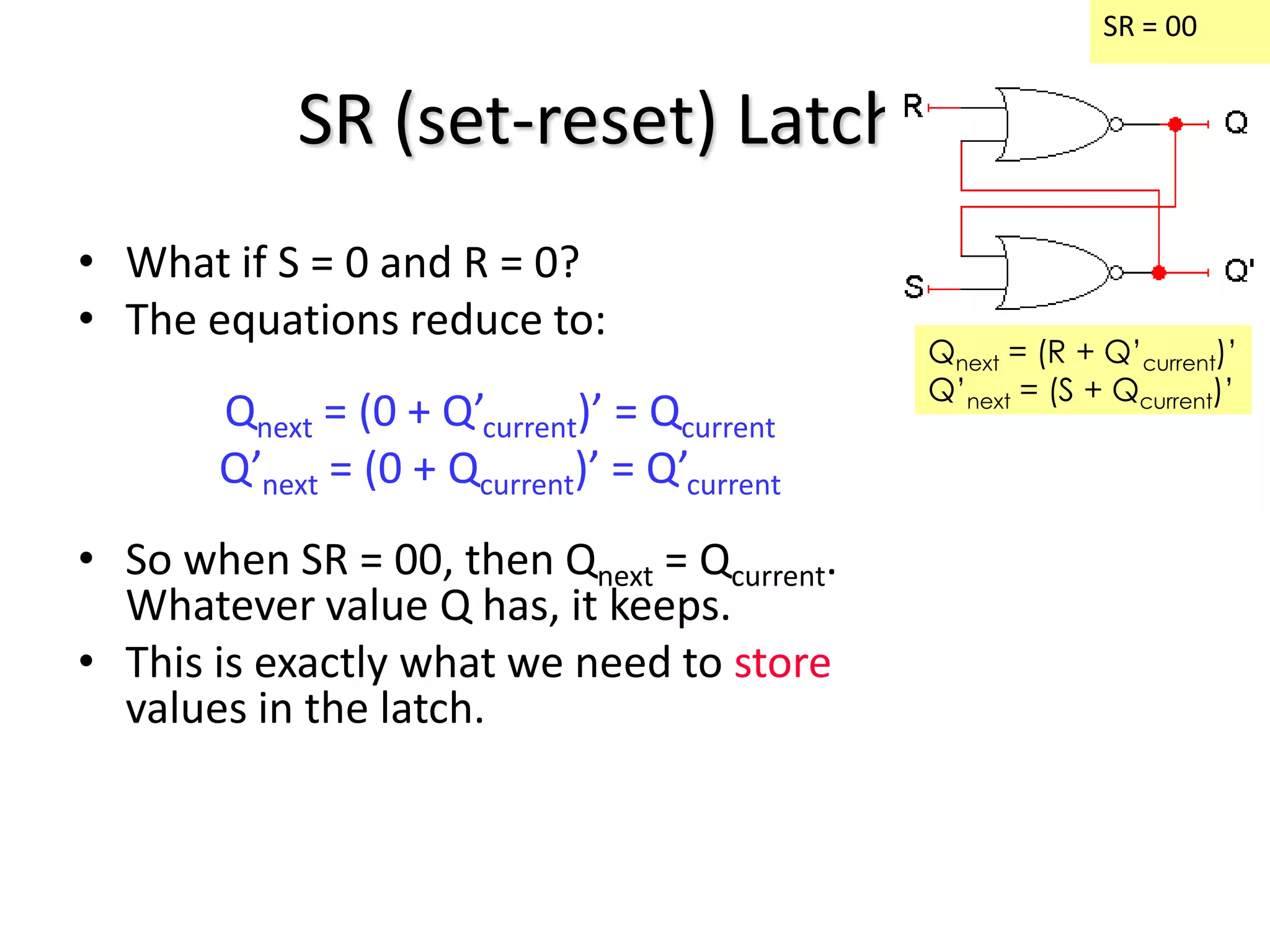
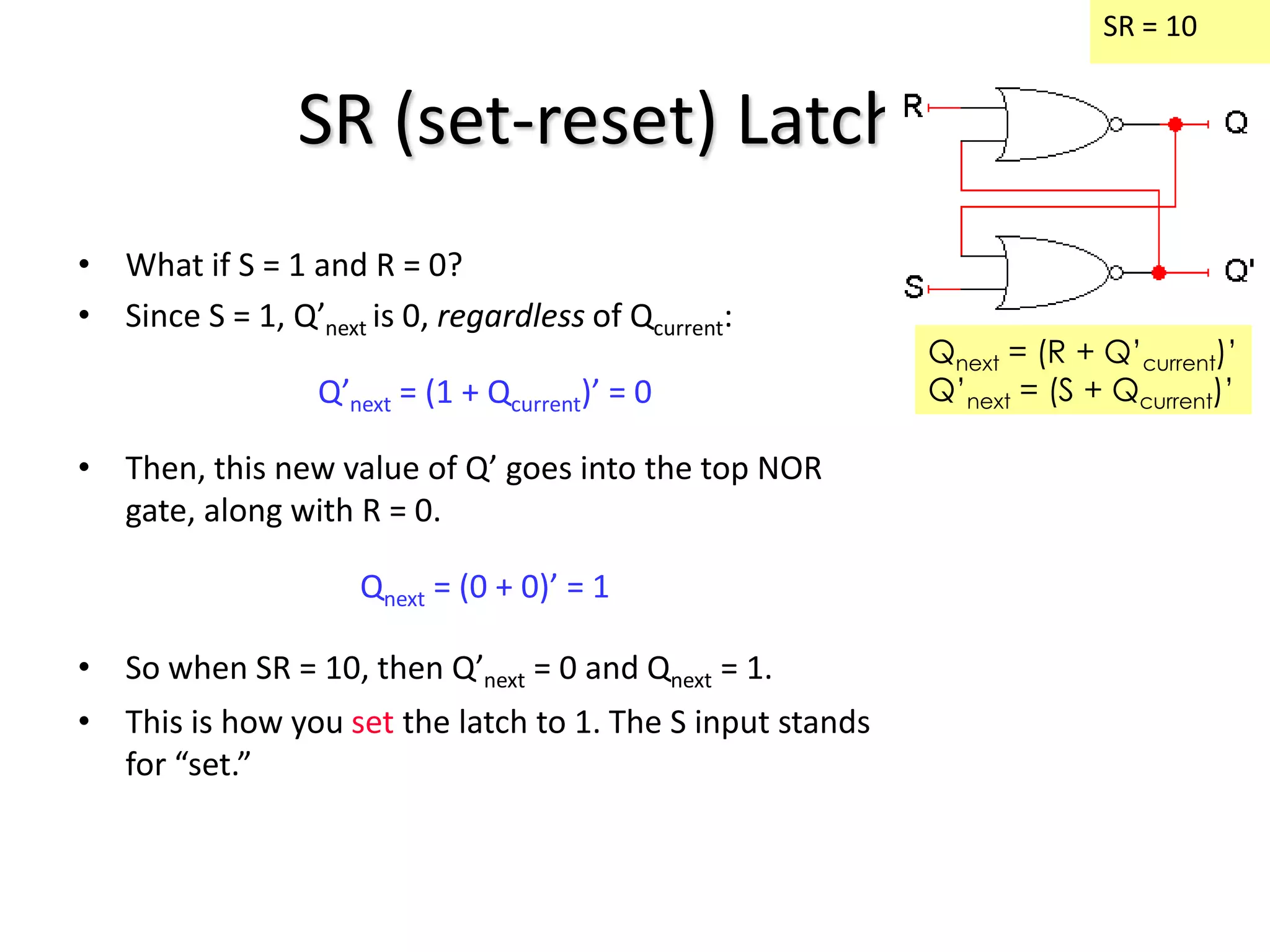
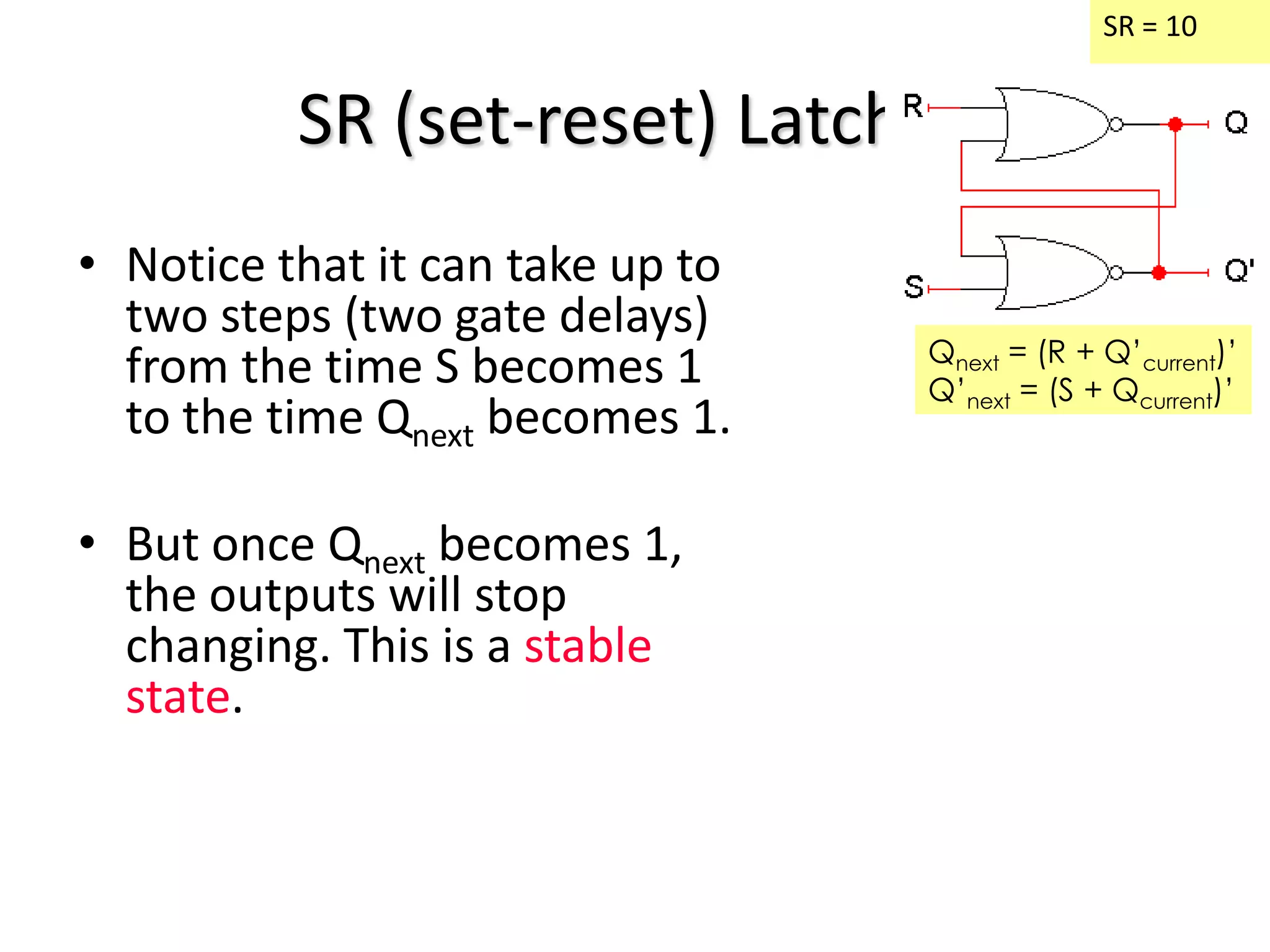
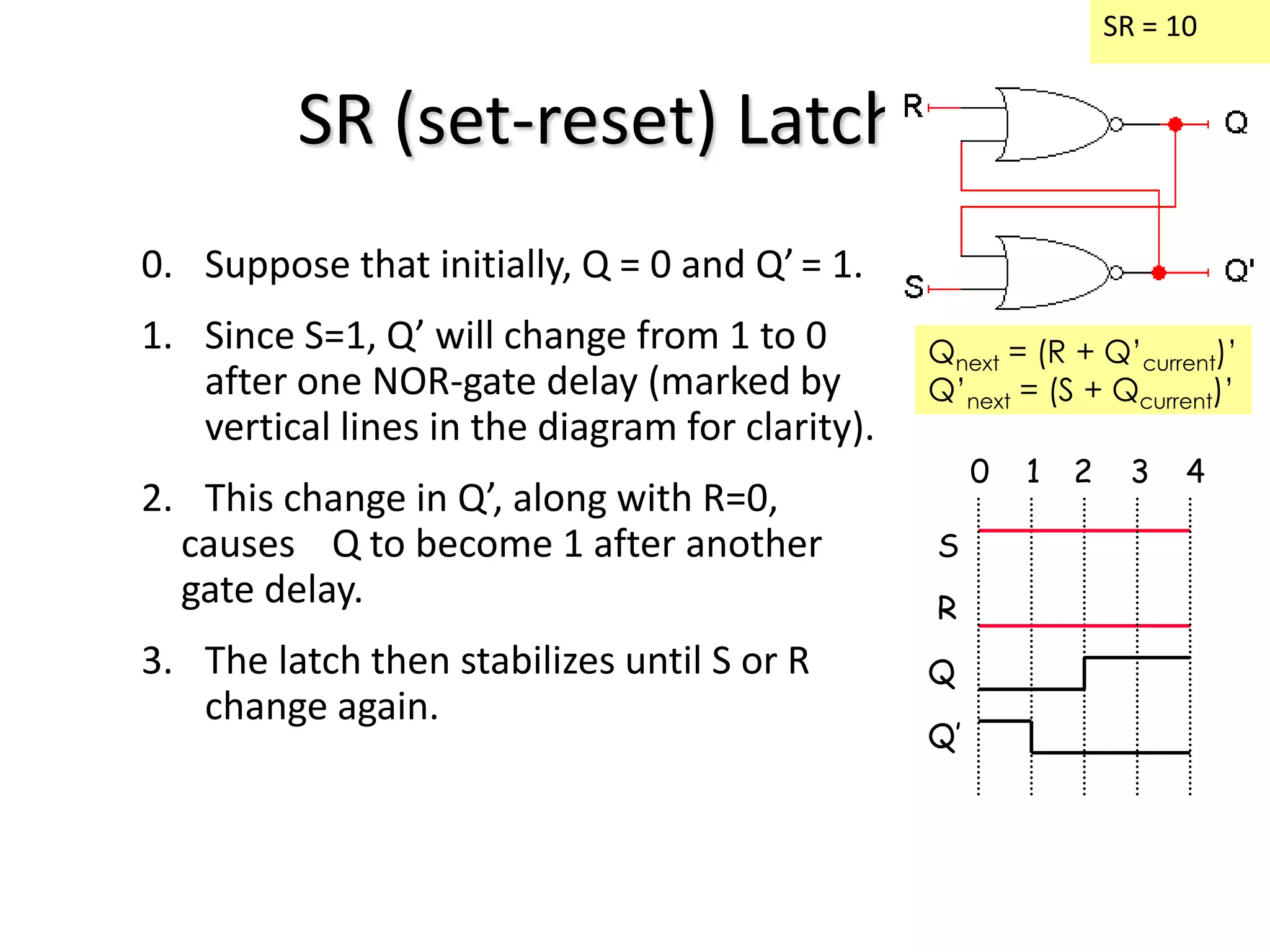
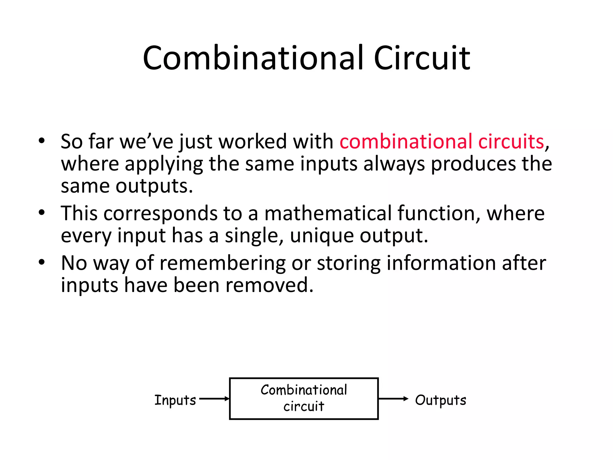
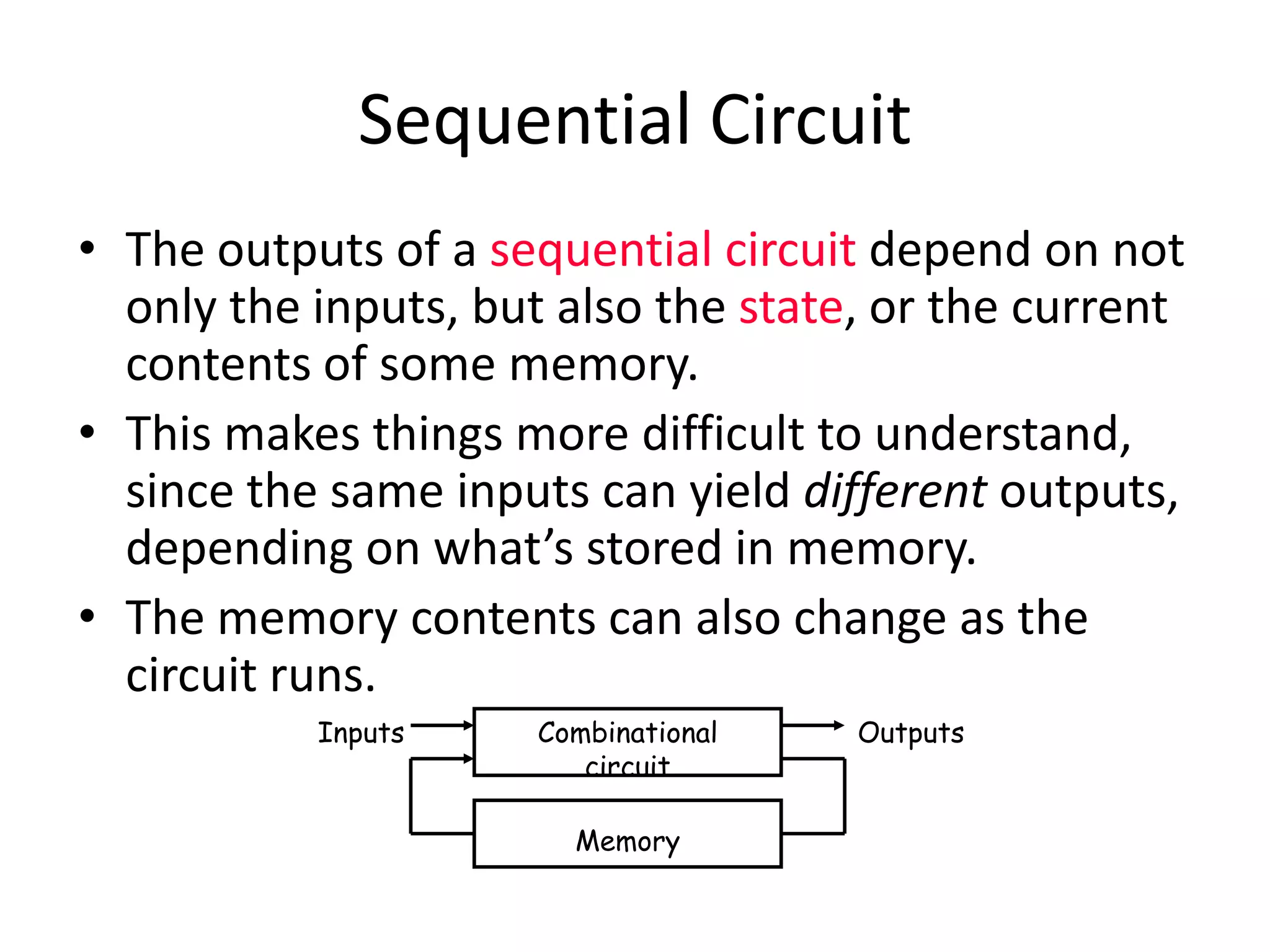
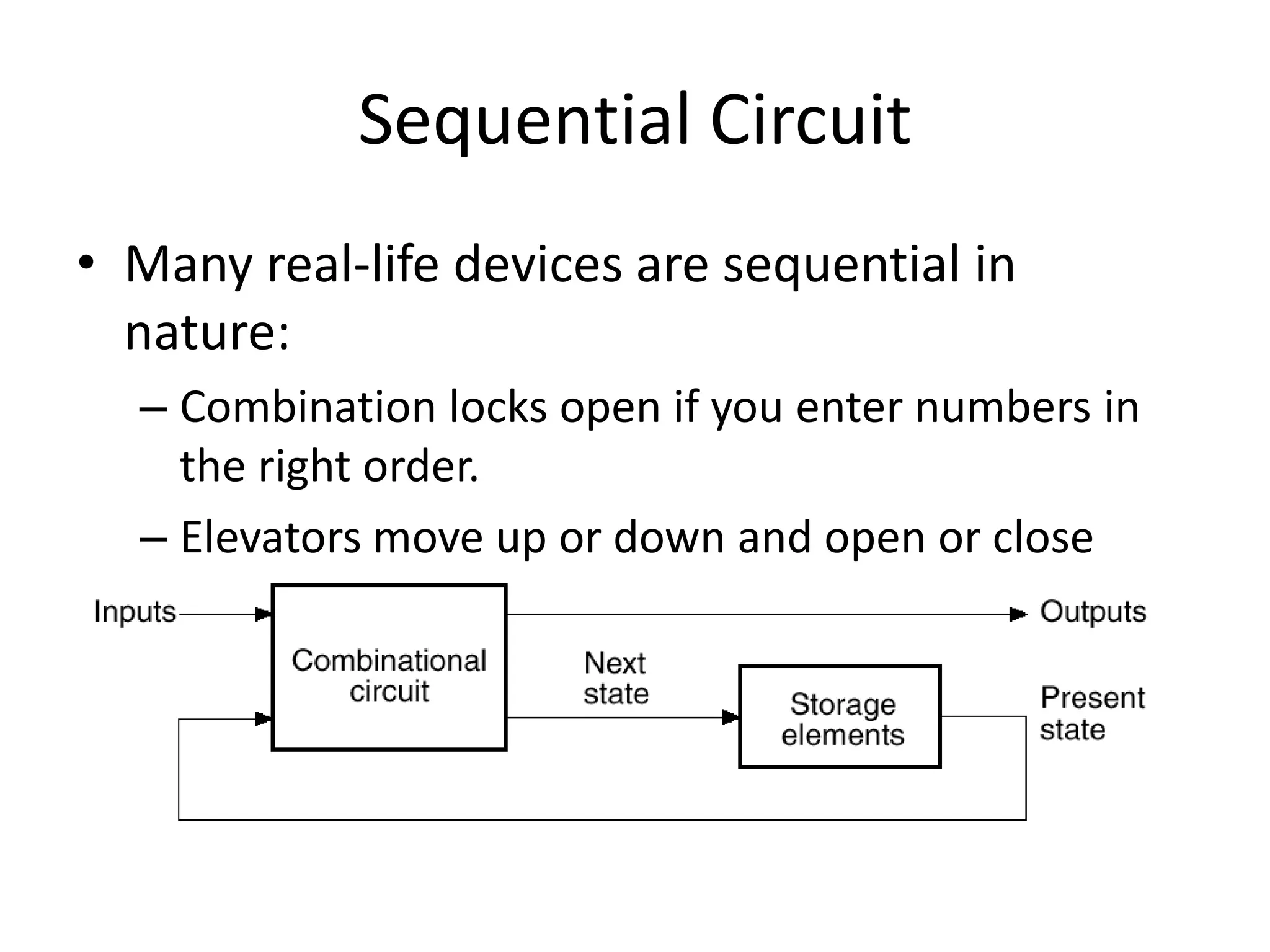
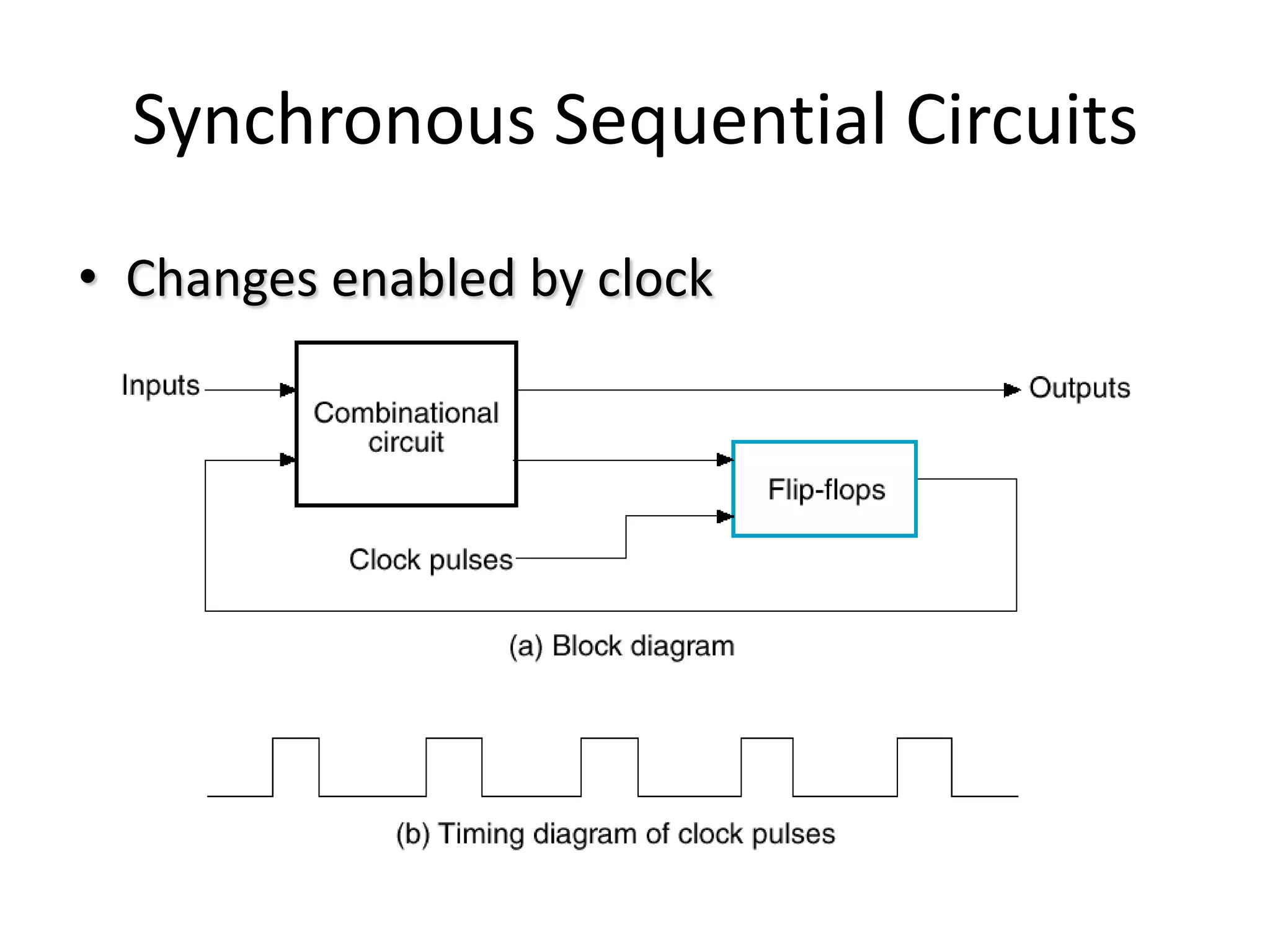
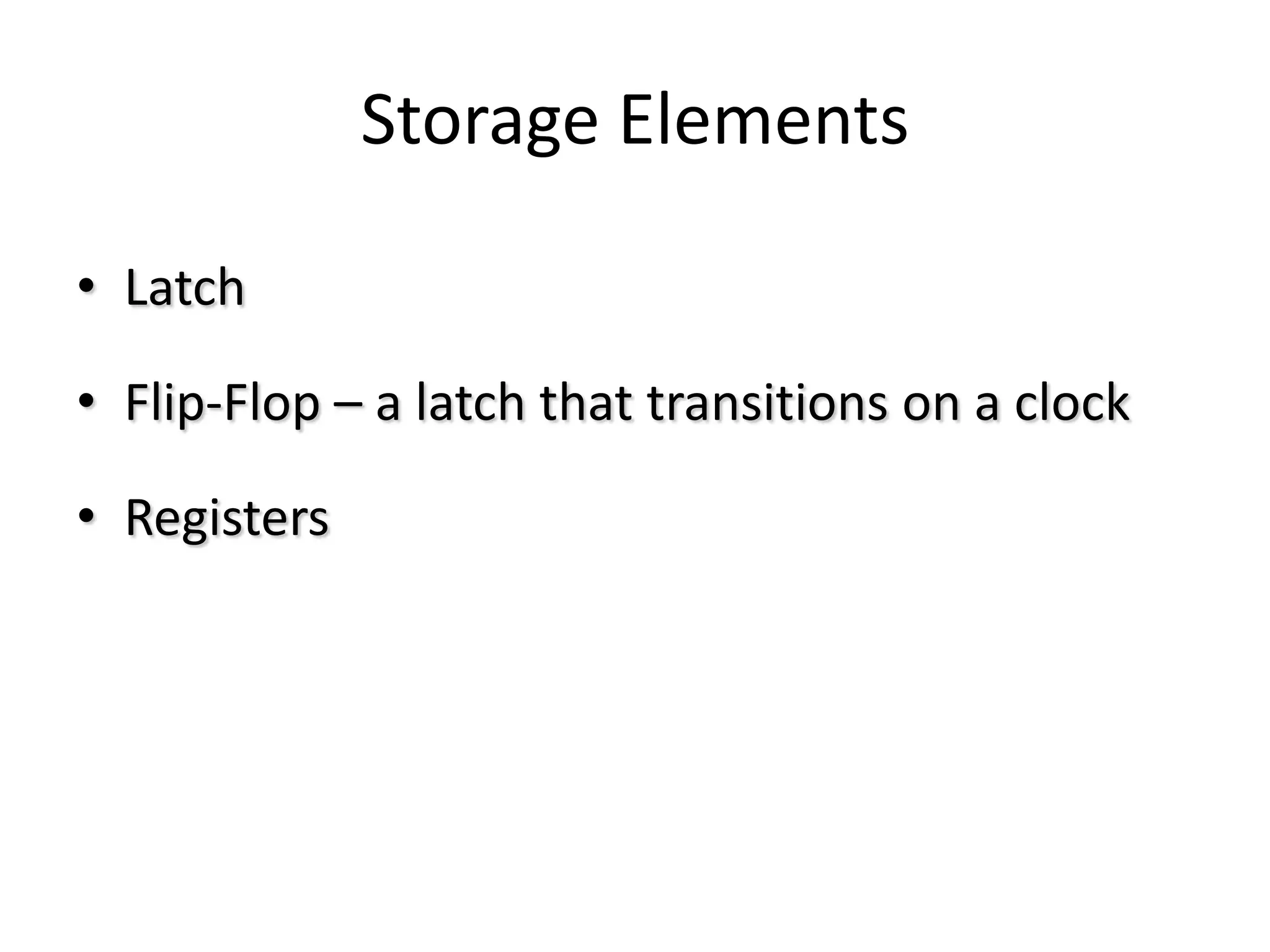
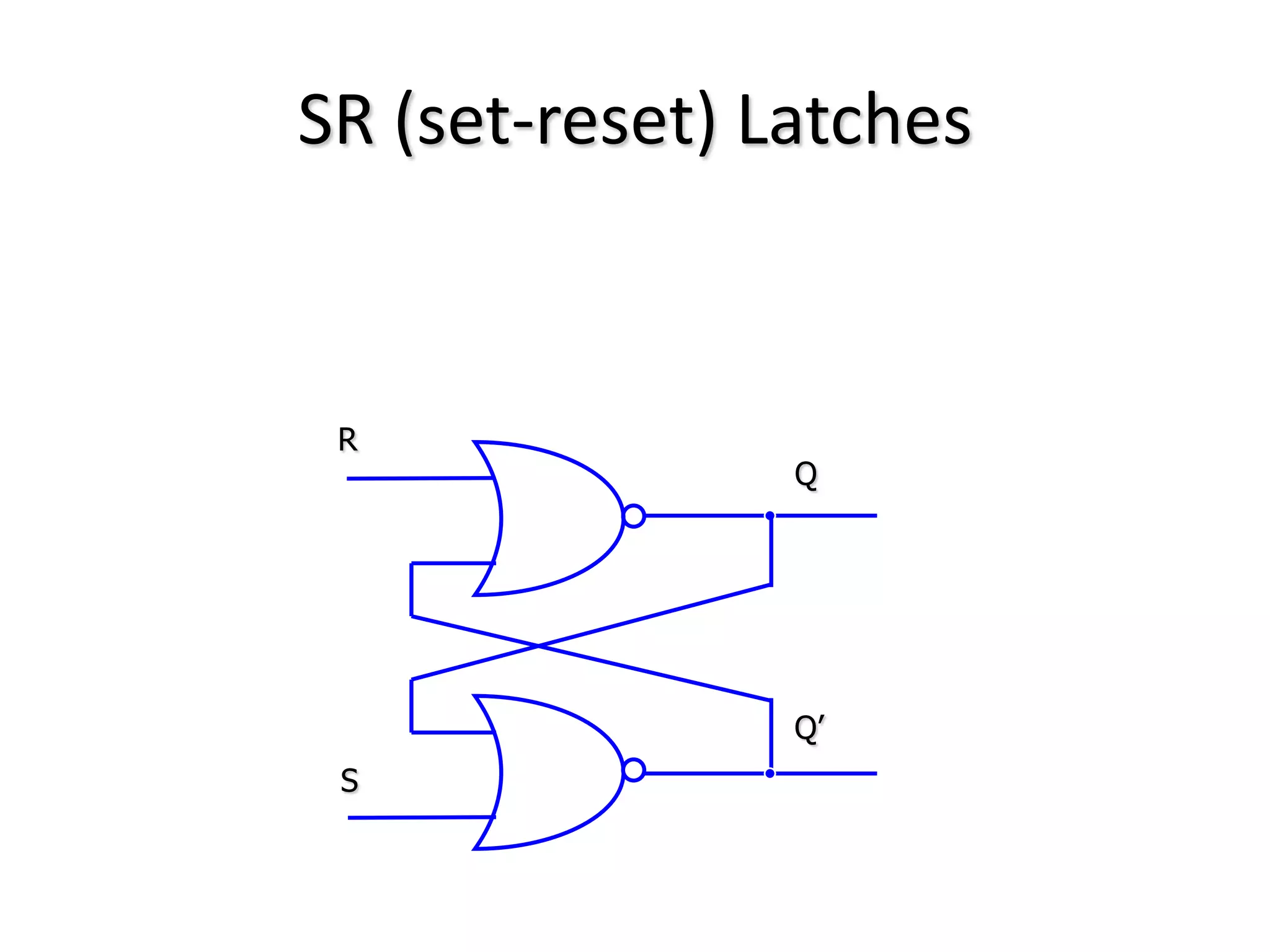
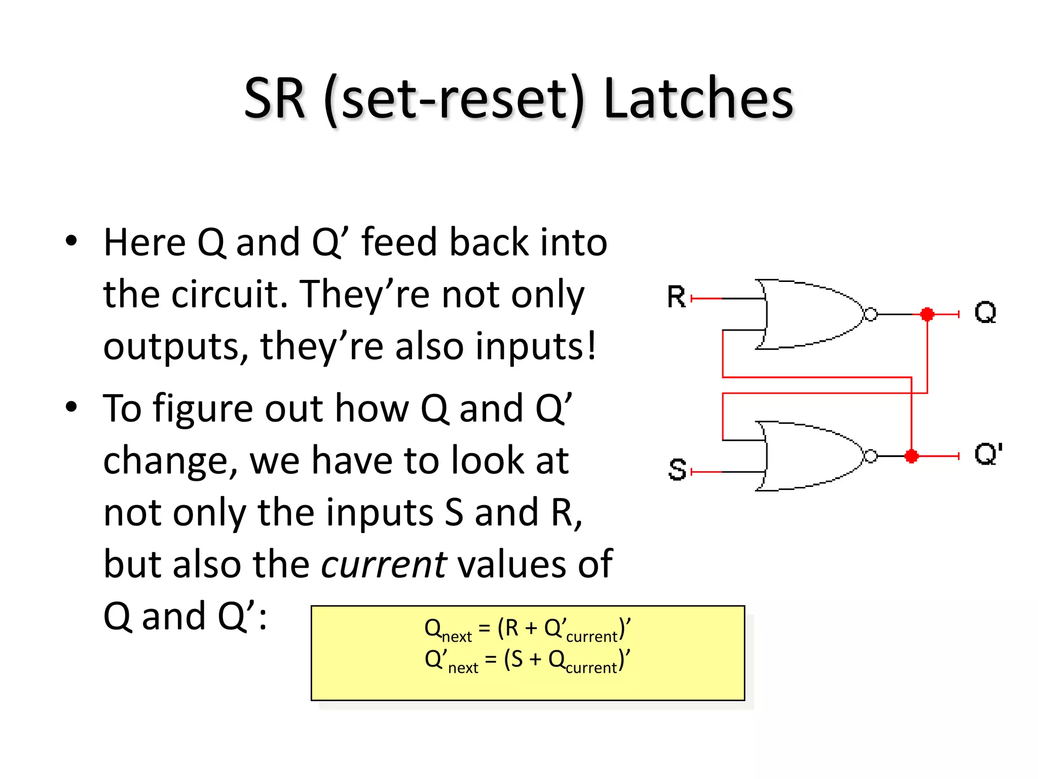
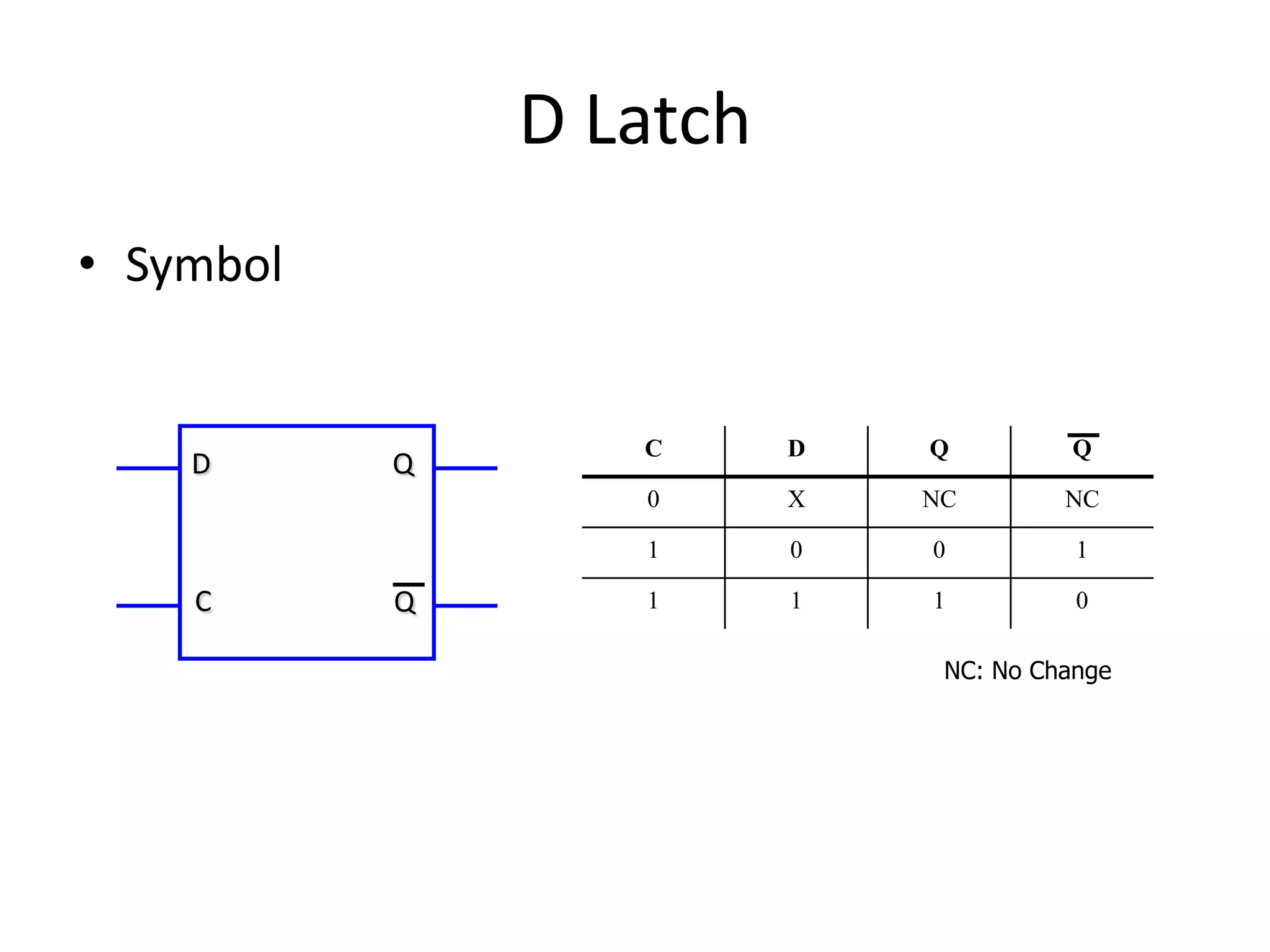
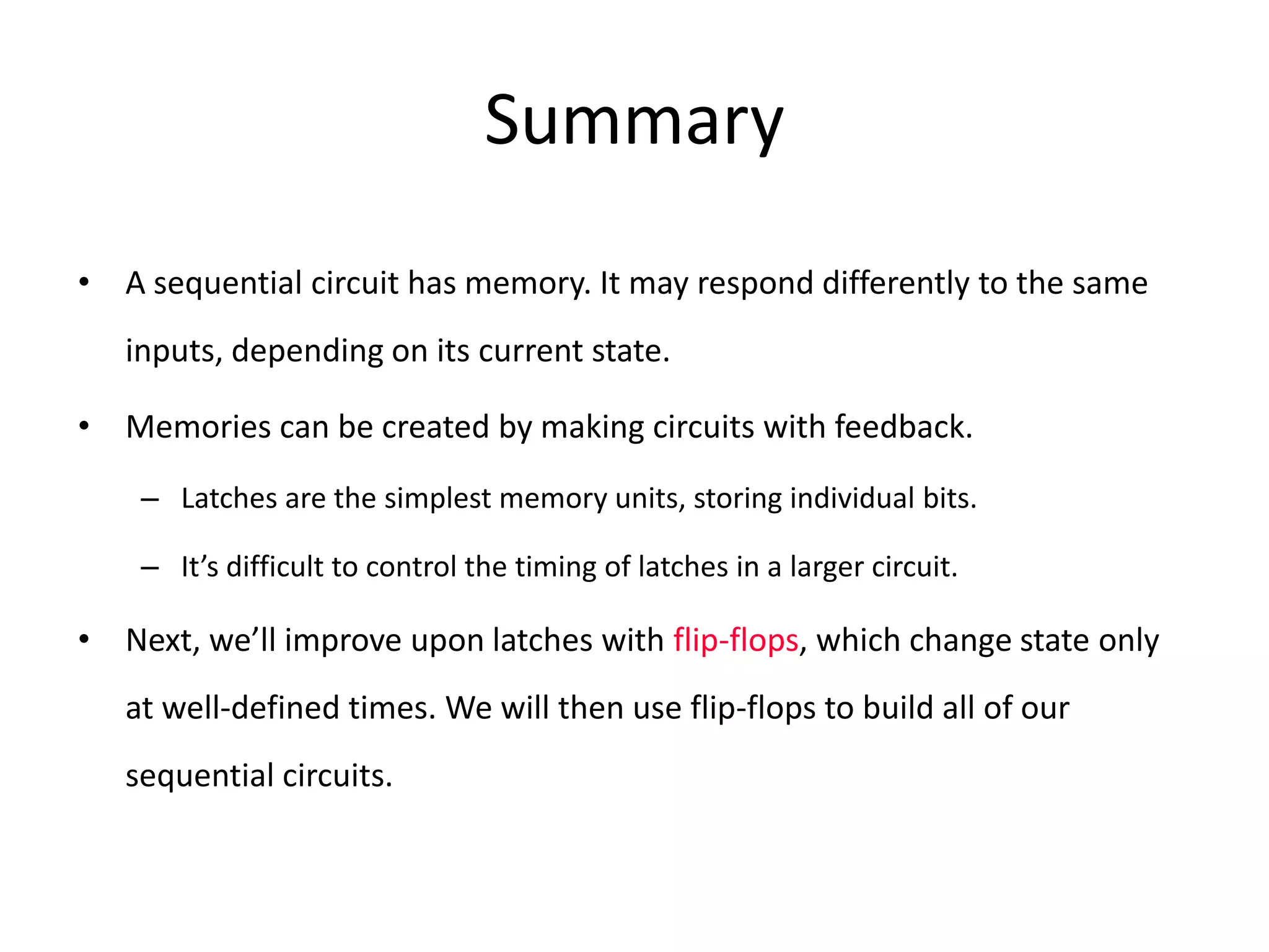
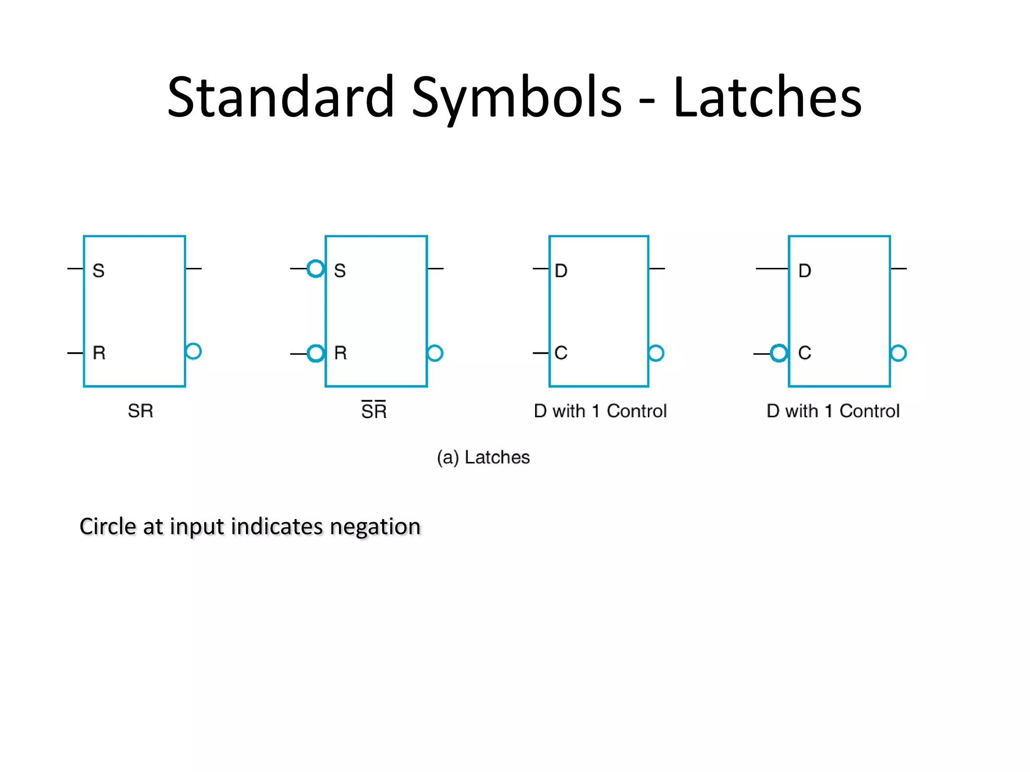
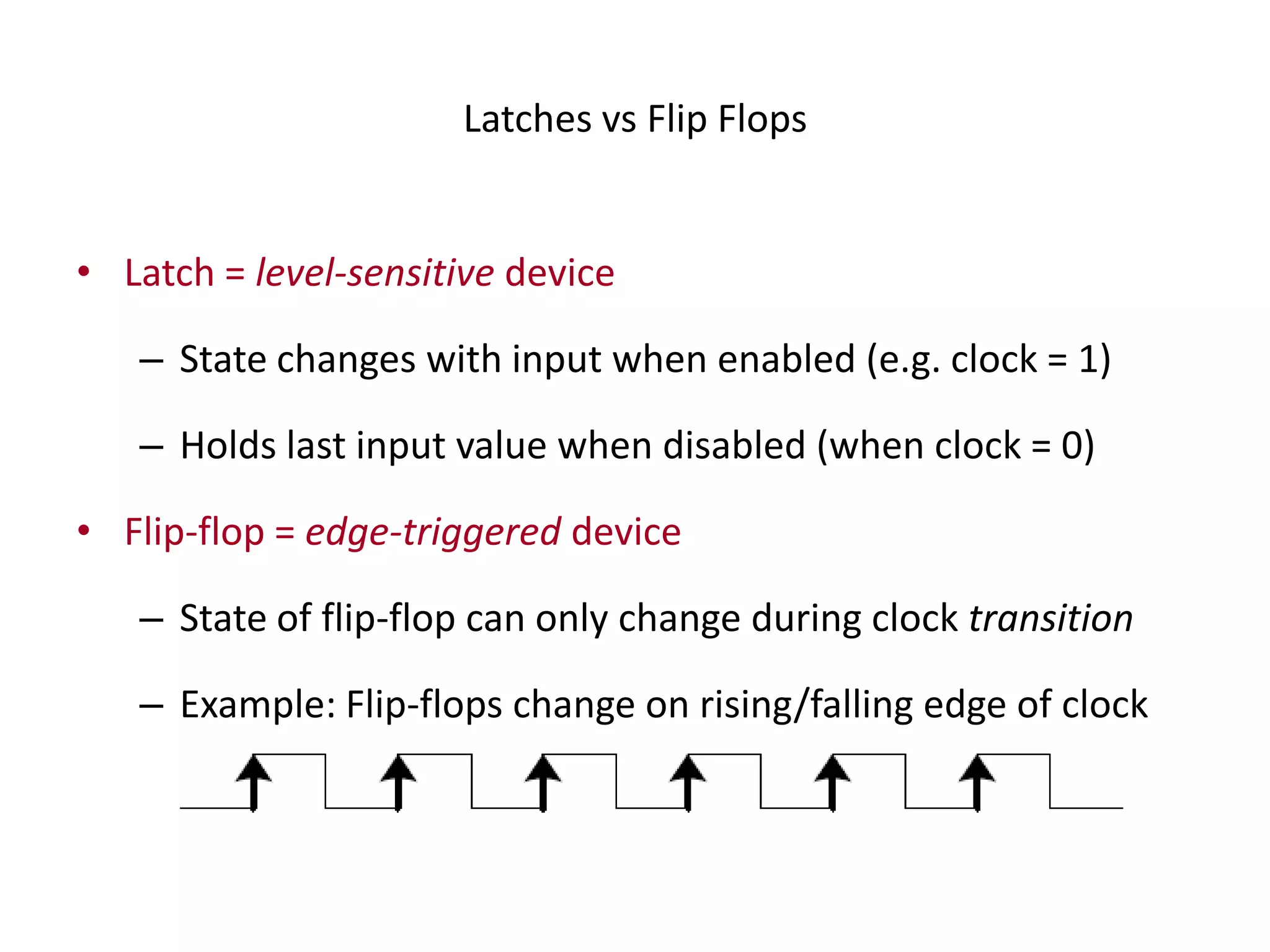
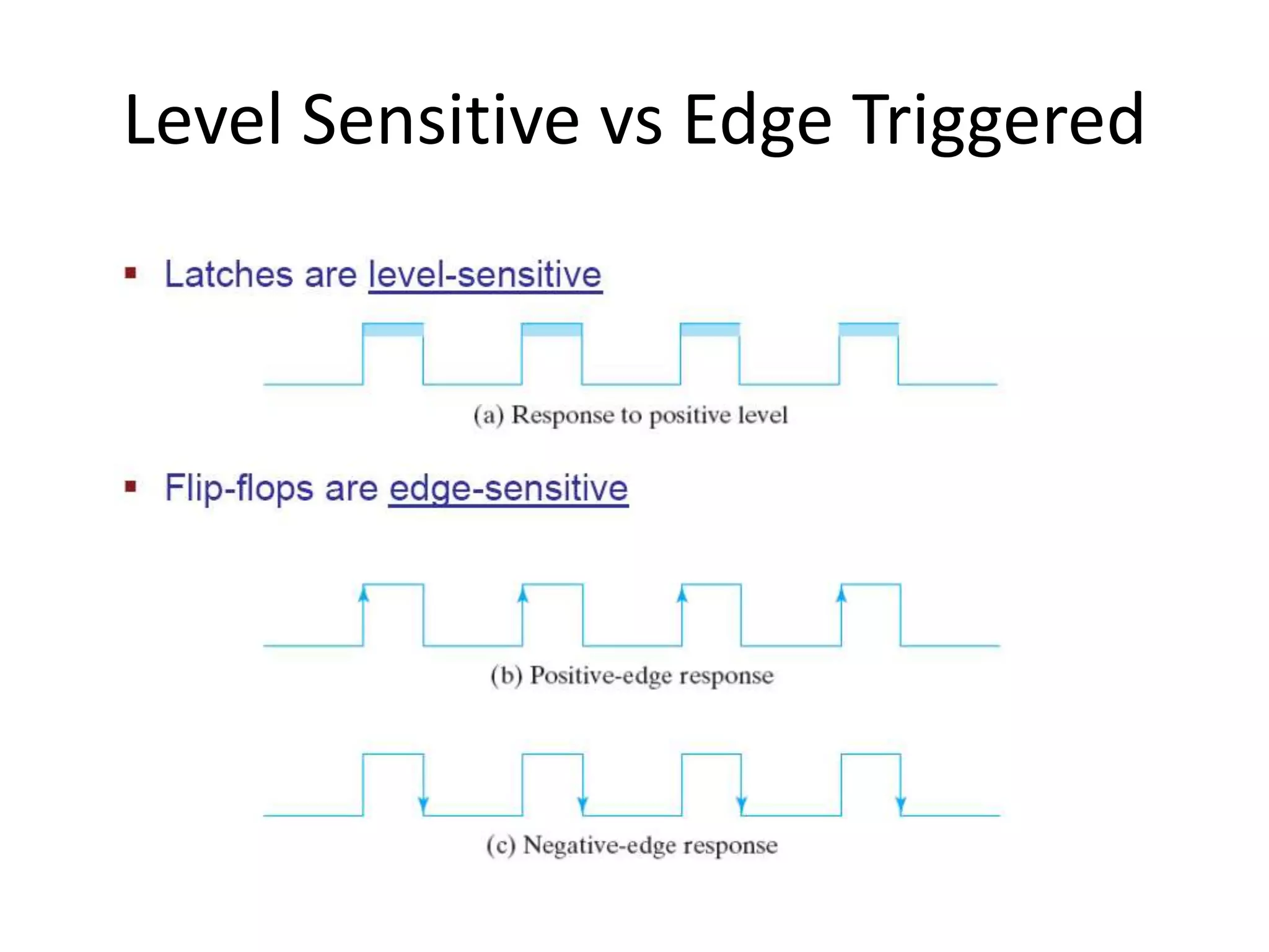
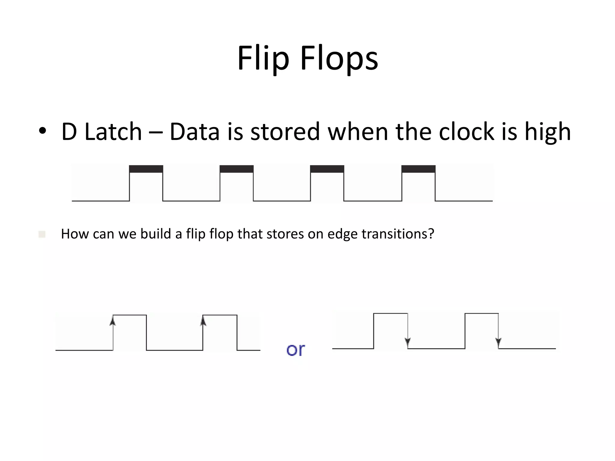
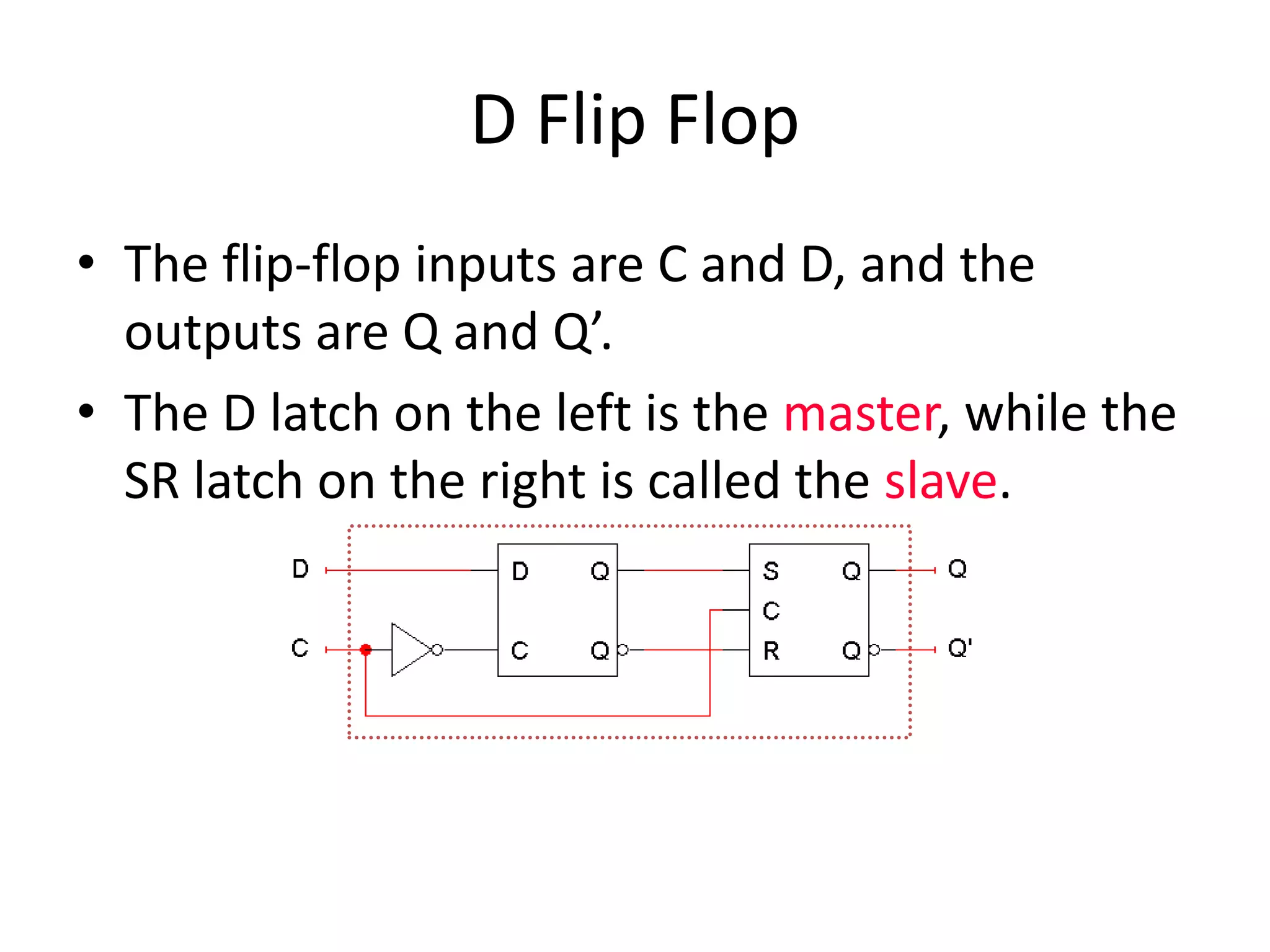
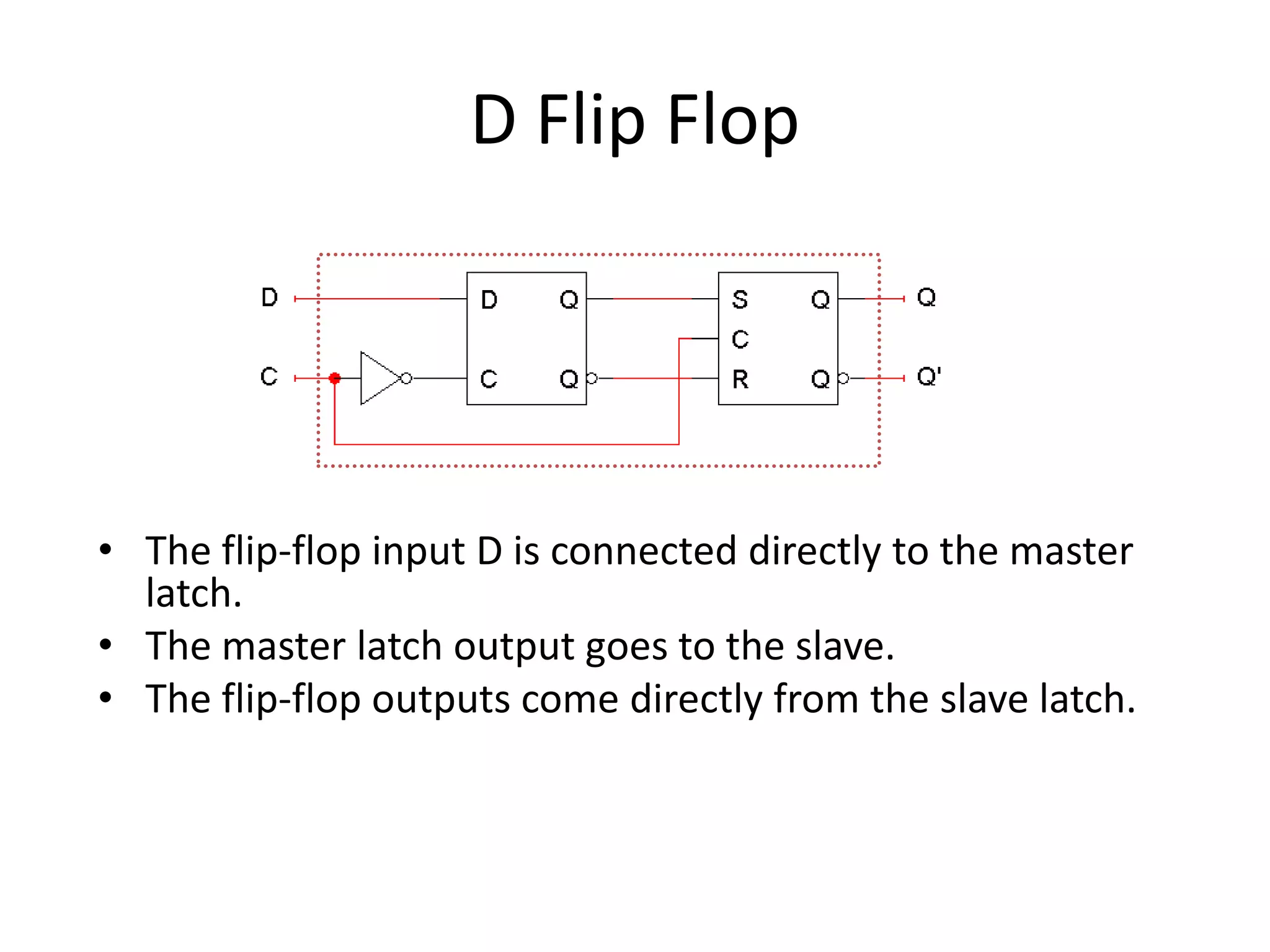
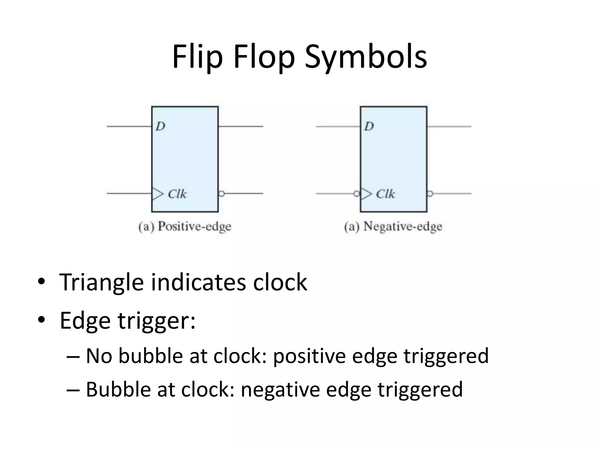
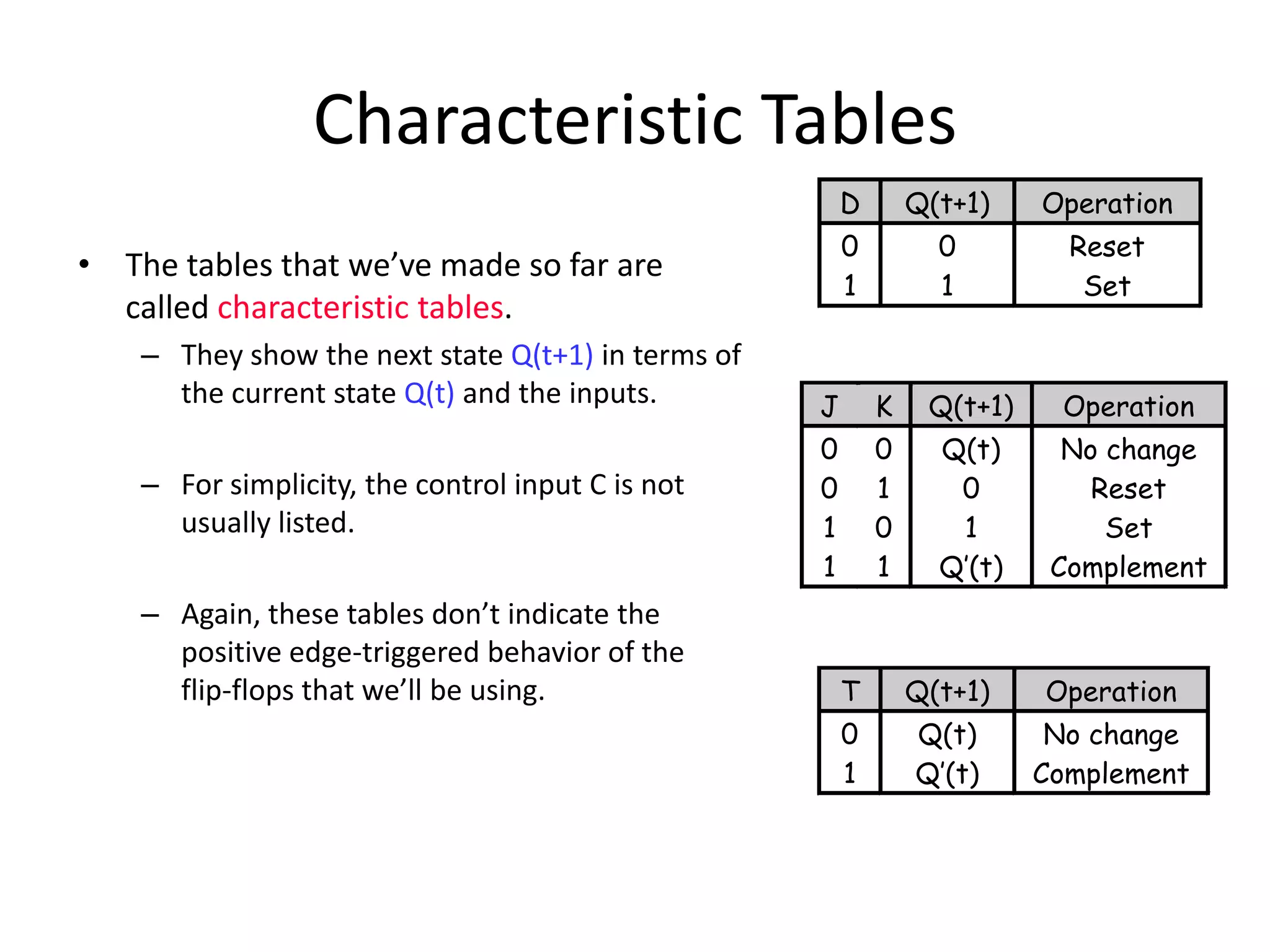
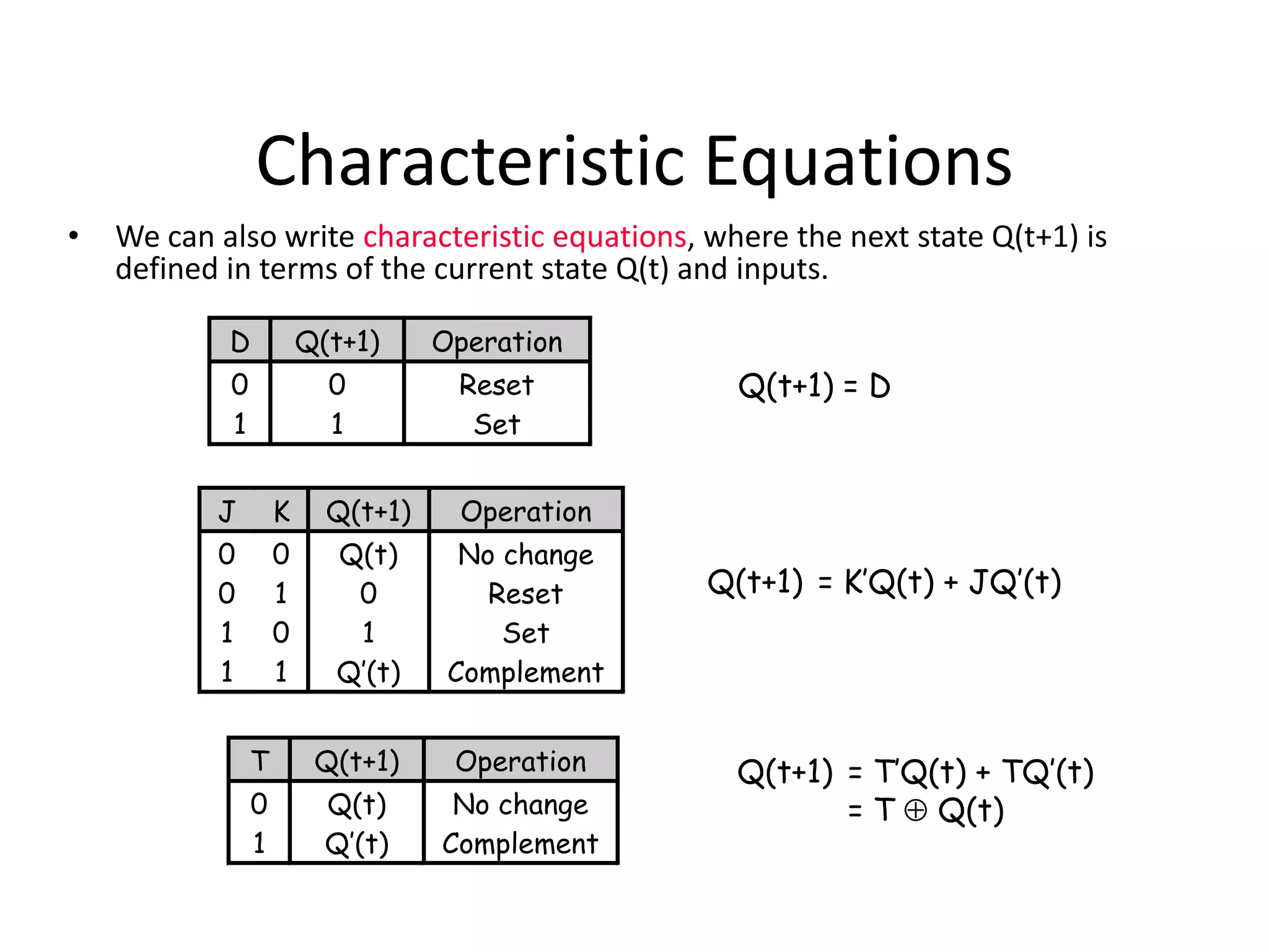
SlideShare a Scribd company logo
1 of 49
Chapter # 5 :
Sequential Circuit
Combinational Circuit
• So far we’ve just worked with combinational circuits,
where applying the same inputs always produces the
same outputs.
• This corresponds to a mathematical function, where
every input has a single, unique output.
• No way of remembering or storing information after
inputs have been removed.
Combinational
circuitInputs Outputs
Sequential Circuit
• The outputs of a sequential circuit depend on not
only the inputs, but also the state, or the current
contents of some memory.
• This makes things more difficult to understand,
since the same inputs can yield different outputs,
depending on what’s stored in memory.
• The memory contents can also change as the
circuit runs.
Combinational
circuit
Inputs
Memory
Outputs
Sequential Circuit
• Many real-life devices are sequential in
nature:
– Combination locks open if you enter numbers in
the right order.
– Elevators move up or down and open or close
depending on the buttons that are pressed on
different floors and in the elevator itself.
Types of Sequential Circuits
• Synchronous
– State changes synchronized by one or more clocks
• Asynchronous
– Timing of changes are independent of any clocks
Synchronous Sequential Circuits
• Changes enabled by clock
Storage Elements
• Latch
• Flip-Flop – a latch that transitions on a clock
• Registers
Memory
• A memory should have at least three properties.
1. It should be able to hold a value.
2. You should be able to read the value that was saved.
3. You should be able to change the value that’s saved.
• We’ll start with the simplest case, a one-bit memory.
1. It should be able to hold a single bit, 0 or 1.
2. You should be able to read the bit that was saved.
3. You should be able to change the value. Since there’s only a single bit, there
are only two choices:
– Set the bit to 1
– Reset, or clear, the bit to 0.
Basic Idea of Storage
• How can a circuit “remember” anything, when
it’s just a bunch of gates that produce outputs
according to the inputs?
• The basic idea is to make a loop, so the circuit
outputs are also inputs.
SR (set-reset) Latches
S
Q
Q’
R
SR (set-reset) Latches
• Here Q and Q’ feed back into
the circuit. They’re not only
outputs, they’re also inputs!
• To figure out how Q and Q’
change, we have to look at
not only the inputs S and R,
but also the current values of
Q and Q’: Qnext = (R + Q’current)’
Q’next = (S + Qcurrent)’
SR (set-reset) Latches
• What if S = 0 and R = 0?
• The equations reduce to:
Qnext = (0 + Q’current)’ = Qcurrent
Q’next = (0 + Qcurrent)’ = Q’current
• So when SR = 00, then Qnext = Qcurrent.
Whatever value Q has, it keeps.
• This is exactly what we need to store
values in the latch.
SR = 00
Qnext = (R + Q’current)’
Q’next = (S + Qcurrent)’
SR (set-reset) Latches
• What if S = 1 and R = 0?
• Since S = 1, Q’next is 0, regardless of Qcurrent:
Q’next = (1 + Qcurrent)’ = 0
• Then, this new value of Q’ goes into the top NOR
gate, along with R = 0.
Qnext = (0 + 0)’ = 1
• So when SR = 10, then Q’next = 0 and Qnext = 1.
• This is how you set the latch to 1. The S input stands
for “set.”
SR = 10
Qnext = (R + Q’current)’
Q’next = (S + Qcurrent)’
SR (set-reset) Latches
• Notice that it can take up to
two steps (two gate delays)
from the time S becomes 1
to the time Qnext becomes 1.
• But once Qnext becomes 1,
the outputs will stop
changing. This is a stable
state.
SR = 10
Qnext = (R + Q’current)’
Q’next = (S + Qcurrent)’
SR (set-reset) Latches
0. Suppose that initially, Q = 0 and Q’= 1.
1. Since S=1, Q’ will change from 1 to 0
after one NOR-gate delay (marked by
vertical lines in the diagram for clarity).
2. This change in Q’, along with R=0,
causes Q to become 1 after another
gate delay.
3. The latch then stabilizes until S or R
change again.
SR = 10
Qnext = (R + Q’current)’
Q’next = (S + Qcurrent)’
S
R
Q
Q’
0 1 2 3 4
SR (set-reset) Latches
• What if S = 0 and R = 1?
• Since R = 1, Qnext is 0, regardless of Qcurrent:
Qnext = (1 + Q’current)’ = 0
• Then, this new value of Q goes into the bottom NOR
gate, where S = 0.
Q’next = (0 + 0)’ = 1
• So when SR = 01, then Qnext = 0 and Q’next = 1.
• This is how you reset, or clear, the latch to 0. The R
input stands for “reset.”
• Again, it can take two gate delays before a change in
R propagates to the output Q’next.
SR = 01
Qnext = (R + Q’current)’
Q’next = (S + Qcurrent)’
SR Latches are Memories
• This little table shows that our latch
provides everything we need in a memory:
we can set it, reset it, and remember the
current value.
S R Q
0 0 No change
0 1 0 (reset)
1 0 1 (set)
 The output Q represents the data stored in the latch. It is sometimes
called the state of the latch.
SR Latches are Memories
• We can expand the table above into a state table,
which explicitly shows that the next values of Q and Q’
depend on their current values, as well as on the inputs
S and R.
Inputs Current Next
S R Q Q’ Q Q’
0 0 0 1 0 1
0 0 1 0 1 0
0 1 0 1 0 1
0 1 1 0 0 1
1 0 0 1 1 0
1 0 1 0 1 0
SR Latches are Sequential
• Notice that for inputs SR = 00, the next
value of Q could be either 0 or 1,
depending on the current value of Q.
• So the same inputs can yield different
outputs, depending on whether the latch
was previously set or reset.
• This is very different from the
combinational circuits that we’ve seen so
far, where the same inputs always yield
the same outputs.
Inputs Current Next
S R Q Q’ Q Q’
0 0 0 1 0 1
0 0 1 0 1 0
0 1 0 1 0 1
0 1 1 0 0 1
1 0 0 1 1 0
1 0 1 0 1 0
S R Q
0 0 No change
0 1 0 (reset)
1 0 1 (set)
What about SR = 11
Qnext = (R + Q’current)’
Q’next = (S + Qcurrent)’
0
0
0
0
0
0
1
1
 Circuit ossiclates between 00 and 11 under the
assumption that both NOR gates have exaclty the
same delay.
 Practically this would not be true so the state
would be either 01 or 10.
 Since we cannot predict it, so the latch is said to
be in undefined state for input 11.
SR Latches
S’R’ Latch
• Similar – made from NANDs
R
Q
QN
S
S’R’ Latch
• This is just like an SR latch, but with inverted inputs, as you can see from the table.
• You can derive this table by writing equations for the outputs in terms of the
inputs and the current state, just as we did for the SR latch.
SR Latch Summary
• SR stands for Set/Reset Latch
– Stores one bit of state (Q)
• Control what value is being stored with S, R
inputs
– Set: Make the output 1 (S = 1, R = 0, Q = 1)
– Reset: Make the output 0 (S = 0, R = 1, Q = 0)
• Behavior undefined/invalid when:
– S = R = 1
S
R Q
Q
SR Latch
Symbol
SR Latch with Control Input
• Notice the hierarchical design!
– The dotted blue box is the S’R’ latch from the previous slide.
– The additional NAND gates are simply used to generate the correct inputs for
the S’R’ latch.
• The control input acts just like an enable.
C S R S’ R’ Q
0 x x 1 1 No change
1 0 0 1 1 No change
1 0 1 1 0 0 (reset)
1 1 0 0 1 1 (set)
1 1 1 0 0 Avoid!
D Latch
• No illegal state
D Latch
• A D latch is based on an S’R’ latch. The additional
gates generate the S’ and R’ signals, based on
inputs D (“data”) and C (“control”).
– When C = 0, S’ and R’ are both 1, so the state Q does
not change.
– When C = 1, the latch output Q will equal the input D.
• No more messing with one input for set and
another input for reset! C D Q
0 x No change
1 0 0
1 1 1
D Latch
• Symbol
D
C
Q
Q
C D Q Q
0 X NC NC
1 0 0 1
1 1 1 0
NC: No Change
Summary
• A sequential circuit has memory. It may respond differently to the same
inputs, depending on its current state.
• Memories can be created by making circuits with feedback.
– Latches are the simplest memory units, storing individual bits.
– It’s difficult to control the timing of latches in a larger circuit.
• Next, we’ll improve upon latches with flip-flops, which change state only
at well-defined times. We will then use flip-flops to build all of our
sequential circuits.
Standard Symbols - Latches
Circle at input indicates negation
Latches vs Flip Flops
• Latch = level-sensitive device
– State changes with input when enabled (e.g. clock = 1)
– Holds last input value when disabled (when clock = 0)
• Flip-flop = edge-triggered device
– State of flip-flop can only change during clock transition
– Example: Flip-flops change on rising/falling edge of clock
Level Sensitive vs Edge Triggered
Flip Flops
• D Latch – Data is stored when the clock is high
 How can we build a flip flop that stores on edge transitions?
D Flip Flop
• The flip-flop inputs are C and D, and the
outputs are Q and Q’.
• The D latch on the left is the master, while the
SR latch on the right is called the slave.
D Flip Flop
• The flip-flop input D is connected directly to the master
latch.
• The master latch output goes to the slave.
• The flip-flop outputs come directly from the slave latch.
D flip-flops when C=0
• The D flip-flop’s control input C enables either
the D latch or the SR latch, but not both.
• When C = 0:
– The master latch is enabled, and it monitors the flip-flop
input D. Whenever D changes, the master’s output
changes too.
– The slave is disabled, so the D latch output has no effect
on it. Thus, the slave just maintains the flip-flop’s current
state.
D flip-flops when C=1
• As soon as C becomes 1, (i.e. on the rising
edge of the clock)
– The master is disabled. Its output will be the last D input value seen just
before C became 1.
– Any subsequent changes to the D input while C = 1 have no effect on the
master latch, which is now disabled.
– The slave latch is enabled. Its state changes to reflect the master’s output,
which again is the D input value from right when C became 1.
Positive Edge Triggering
• The D flip-flop’s behavior is similar to that of a D latch
except for the positive edge-triggered nature, which is
not explicit in this table.
C D Q
0 x No change
1 0 0 (reset)
1 1 1 (set)
 This is called a positive edge-triggered flip-flop.
 The flip-flop output Q changes only after the positive edge of C.
 The change is based on the flip-flop input values that were present right at the
positive edge of the clock signal.
D Flip Flop
• Is this +ve or –ve edge-triggered?
Flip Flop Symbols
• Triangle indicates clock
• Edge trigger:
– No bubble at clock: positive edge triggered
– Bubble at clock: negative edge triggered
Flip Flop Variations
• A JK flip-flop has inputs that act like S and R,
but the inputs JK=11 are used to complement
the flip-flop’s current state
C J K Qnext
0 x x No change
1 0 0 No change
1 0 1 0 (reset)
1 1 0 1 (set)
1 1 1 Q’current
JK Flip Flop
Created from D flip flop
D = JQ’+K’Q
JK Flip Flop
Created from D flip flop
D = JQ’+K’Q
J=1 & K=0
D = Q’+Q = 1
Flip flop is SET
J=0 & K=1
D = 0+0 = 0
Flip flop is RESET
J=1 & K=1
D = Q’+0 = Q’
Output is Complemented
J=0 & K=0
D = Q+0 = Q
Output unchanged
T (Toggle) Flip Flop
• A T (toggle) flip-flop can only maintain or
complement its current state.
C T Qnext
0 x No change
1 0 No change
1 1 Q’current
T (Toggle) Flip Flop
Created from JK flip flop
T (Toggle) Flip Flop
When T = 0, J=0 & K=0
Output is unchanged
When T = 1, J=1 & K=1
Output is complemented
Created from JK flip flop
T (Toggle) Flip Flop
Created from D flip flop
D = TQ’+T’Q
When T = 0, D=Q
Output is unchanged
When T = 1, D=Q’
Output is complemented
Characteristic Tables
• The tables that we’ve made so far are
called characteristic tables.
– They show the next state Q(t+1) in terms of
the current state Q(t) and the inputs.
– For simplicity, the control input C is not
usually listed.
– Again, these tables don’t indicate the
positive edge-triggered behavior of the
flip-flops that we’ll be using.
D Q(t+1) Operation
0 0 Reset
1 1 Set
T Q(t+1) Operation
0 Q(t) No change
1 Q’(t) Complement
J K Q(t+1) Operation
0 0 Q(t) No change
0 1 0 Reset
1 0 1 Set
1 1 Q’(t) Complement
Characteristic Equations
• We can also write characteristic equations, where the next state Q(t+1) is
defined in terms of the current state Q(t) and inputs.
D Q(t+1) Operation
0 0 Reset
1 1 Set
J K Q(t+1) Operation
0 0 Q(t) No change
0 1 0 Reset
1 0 1 Set
1 1 Q’(t) Complement
Q(t+1) = D
Q(t+1) = K’Q(t) + JQ’(t)
Q(t+1) = T’Q(t) + TQ’(t)
= T Q(t)
T Q(t+1) Operation
0 Q(t) No change
1 Q’(t) Complement

More Related Content

What's hot

Electrónica digital: Elementos de memoria y análisis de circuitos secuenciales
Electrónica digital: Elementos de memoria y análisis de circuitos secuenciales Electrónica digital: Elementos de memoria y análisis de circuitos secuenciales
Electrónica digital: Elementos de memoria y análisis de circuitos secuenciales
SANTIAGO PABLO ALBERTO
 

What's hot (20)

BEEE FLIP FLOP & REGISTERS
BEEE FLIP FLOP & REGISTERSBEEE FLIP FLOP & REGISTERS
BEEE FLIP FLOP & REGISTERS
 
Chapter 6: Sequential Logic
Chapter 6: Sequential LogicChapter 6: Sequential Logic
Chapter 6: Sequential Logic
 
Sequential circuits in Digital Electronics
Sequential circuits in Digital ElectronicsSequential circuits in Digital Electronics
Sequential circuits in Digital Electronics
 
Latches & flip flop
Latches & flip flopLatches & flip flop
Latches & flip flop
 
Memory elements
Memory elementsMemory elements
Memory elements
 
Digital alarm clock- Digital design- Design assignment
Digital alarm clock- Digital design- Design assignmentDigital alarm clock- Digital design- Design assignment
Digital alarm clock- Digital design- Design assignment
 
Sequential circuits
Sequential circuitsSequential circuits
Sequential circuits
 
Sequential Logic Circuit
Sequential Logic CircuitSequential Logic Circuit
Sequential Logic Circuit
 
Latches and flip flops
Latches and flip flopsLatches and flip flops
Latches and flip flops
 
Cs1104 11
Cs1104 11Cs1104 11
Cs1104 11
 
Latches
LatchesLatches
Latches
 
Chapter 3
Chapter 3Chapter 3
Chapter 3
 
B sc cs i bo-de u-iv sequential circuit
B sc cs i bo-de u-iv sequential circuitB sc cs i bo-de u-iv sequential circuit
B sc cs i bo-de u-iv sequential circuit
 
Group 10 flip flop and rs latch 1
Group 10 flip flop and rs latch 1Group 10 flip flop and rs latch 1
Group 10 flip flop and rs latch 1
 
Traffic
TrafficTraffic
Traffic
 
Flipflop r012
Flipflop   r012Flipflop   r012
Flipflop r012
 
latches
 latches latches
latches
 
B sc3 unit 5 sequencial lc
B sc3 unit 5 sequencial lcB sc3 unit 5 sequencial lc
B sc3 unit 5 sequencial lc
 
Electrónica digital: Elementos de memoria y análisis de circuitos secuenciales
Electrónica digital: Elementos de memoria y análisis de circuitos secuenciales Electrónica digital: Elementos de memoria y análisis de circuitos secuenciales
Electrónica digital: Elementos de memoria y análisis de circuitos secuenciales
 
Logic design alexander1 christopher
Logic design alexander1  christopherLogic design alexander1  christopher
Logic design alexander1 christopher
 

Viewers also liked

Priprincipl telecommunications and networks es learning objectivesnciples lea...
Priprincipl telecommunications and networks es learning objectivesnciples lea...Priprincipl telecommunications and networks es learning objectivesnciples lea...
Priprincipl telecommunications and networks es learning objectivesnciples lea...
Zain Ul Abedeen
 
Why learn about the internet 7
Why learn about the internet 7Why learn about the internet 7
Why learn about the internet 7
Zain Ul Abedeen
 
Как монетизировать 100% доступного инвентаря на сайте?
Как монетизировать 100% доступного инвентаря на сайте?Как монетизировать 100% доступного инвентаря на сайте?
Как монетизировать 100% доступного инвентаря на сайте?
Maksim Krasovskiy
 
Why learn about the internet 7
Why learn about the internet 7Why learn about the internet 7
Why learn about the internet 7
Zain Ul Abedeen
 
Priprincipl telecommunications and networks es learning objectivesnciples lea...
Priprincipl telecommunications and networks es learning objectivesnciples lea...Priprincipl telecommunications and networks es learning objectivesnciples lea...
Priprincipl telecommunications and networks es learning objectivesnciples lea...
Zain Ul Abedeen
 

Viewers also liked (15)

Lec 25 26_27
Lec 25 26_27Lec 25 26_27
Lec 25 26_27
 
Priprincipl telecommunications and networks es learning objectivesnciples lea...
Priprincipl telecommunications and networks es learning objectivesnciples lea...Priprincipl telecommunications and networks es learning objectivesnciples lea...
Priprincipl telecommunications and networks es learning objectivesnciples lea...
 
Медиа-кит Video SSP Advark для рекламных агентств
Медиа-кит Video SSP Advark для рекламных агентствМедиа-кит Video SSP Advark для рекламных агентств
Медиа-кит Video SSP Advark для рекламных агентств
 
Why learn about the internet 7
Why learn about the internet 7Why learn about the internet 7
Why learn about the internet 7
 
Как монетизировать 100% доступного инвентаря на сайте?
Как монетизировать 100% доступного инвентаря на сайте?Как монетизировать 100% доступного инвентаря на сайте?
Как монетизировать 100% доступного инвентаря на сайте?
 
Advark - Video advertising platform
Advark - Video advertising platformAdvark - Video advertising platform
Advark - Video advertising platform
 
Why learn about the internet 7
Why learn about the internet 7Why learn about the internet 7
Why learn about the internet 7
 
Priprincipl telecommunications and networks es learning objectivesnciples lea...
Priprincipl telecommunications and networks es learning objectivesnciples lea...Priprincipl telecommunications and networks es learning objectivesnciples lea...
Priprincipl telecommunications and networks es learning objectivesnciples lea...
 
Advark - Video Supply Side Platform
Advark - Video Supply Side PlatformAdvark - Video Supply Side Platform
Advark - Video Supply Side Platform
 
Business Benefits of Cloud Computing to Indian IT Service
Business Benefits of Cloud Computing to Indian IT ServiceBusiness Benefits of Cloud Computing to Indian IT Service
Business Benefits of Cloud Computing to Indian IT Service
 
Advark - платформа управления видеорекламой
Advark - платформа управления видеорекламойAdvark - платформа управления видеорекламой
Advark - платформа управления видеорекламой
 
Dld
DldDld
Dld
 
Lec20
Lec20Lec20
Lec20
 
Dehesa de 900 has con una gran casa en la Sierra Norte de Sevilla
Dehesa de 900 has con una gran casa en la Sierra Norte de SevillaDehesa de 900 has con una gran casa en la Sierra Norte de Sevilla
Dehesa de 900 has con una gran casa en la Sierra Norte de Sevilla
 
Bis 2016 03 especial 15 pisos con encanto 2
Bis 2016 03 especial 15 pisos con encanto 2Bis 2016 03 especial 15 pisos con encanto 2
Bis 2016 03 especial 15 pisos con encanto 2
 

Similar to Sequential

08 Latches and Flipflops.pdf
08 Latches and Flipflops.pdf08 Latches and Flipflops.pdf
08 Latches and Flipflops.pdf
DSOOP
 
Digital_Electronics_Module_4_Sequential_Circuits v0.6.pptx
Digital_Electronics_Module_4_Sequential_Circuits v0.6.pptxDigital_Electronics_Module_4_Sequential_Circuits v0.6.pptx
Digital_Electronics_Module_4_Sequential_Circuits v0.6.pptx
UtsavDas21
 
Introduction to Sequential DevicesChapter 66.1 M.docx
Introduction to Sequential DevicesChapter 66.1 M.docxIntroduction to Sequential DevicesChapter 66.1 M.docx
Introduction to Sequential DevicesChapter 66.1 M.docx
bagotjesusa
 

Similar to Sequential (20)

Sequential logic circuits flip-flop pt 1
Sequential logic circuits   flip-flop pt 1Sequential logic circuits   flip-flop pt 1
Sequential logic circuits flip-flop pt 1
 
Digital Electronics Unit_3.pptx
Digital Electronics Unit_3.pptxDigital Electronics Unit_3.pptx
Digital Electronics Unit_3.pptx
 
lec7.ppt
lec7.pptlec7.ppt
lec7.ppt
 
IS 151 Lecture 10
IS 151 Lecture 10IS 151 Lecture 10
IS 151 Lecture 10
 
Flipflops and Excitation tables of flipflops
Flipflops and Excitation tables of flipflopsFlipflops and Excitation tables of flipflops
Flipflops and Excitation tables of flipflops
 
Latch Introduction & RS Latch
Latch Introduction &  RS LatchLatch Introduction &  RS Latch
Latch Introduction & RS Latch
 
08 Latches and Flipflops.pdf
08 Latches and Flipflops.pdf08 Latches and Flipflops.pdf
08 Latches and Flipflops.pdf
 
best slides latches.pdf
best slides latches.pdfbest slides latches.pdf
best slides latches.pdf
 
Sequential circuit
Sequential circuitSequential circuit
Sequential circuit
 
Flip flops
Flip flopsFlip flops
Flip flops
 
Digital_Electronics_Module_4_Sequential_Circuits v0.6.pptx
Digital_Electronics_Module_4_Sequential_Circuits v0.6.pptxDigital_Electronics_Module_4_Sequential_Circuits v0.6.pptx
Digital_Electronics_Module_4_Sequential_Circuits v0.6.pptx
 
UNIT - III.pptx
UNIT - III.pptxUNIT - III.pptx
UNIT - III.pptx
 
Sequential circuit latchs and Flip-Flops.
Sequential circuit latchs and Flip-Flops.Sequential circuit latchs and Flip-Flops.
Sequential circuit latchs and Flip-Flops.
 
Logic Gate
Logic GateLogic Gate
Logic Gate
 
Flip flop
Flip flopFlip flop
Flip flop
 
Latches and flip flops
Latches and flip flopsLatches and flip flops
Latches and flip flops
 
Latch and Flipflop.pptx
Latch and Flipflop.pptxLatch and Flipflop.pptx
Latch and Flipflop.pptx
 
Latches and flip flop
Latches and flip flopLatches and flip flop
Latches and flip flop
 
Introduction to Sequential DevicesChapter 66.1 M.docx
Introduction to Sequential DevicesChapter 66.1 M.docxIntroduction to Sequential DevicesChapter 66.1 M.docx
Introduction to Sequential DevicesChapter 66.1 M.docx
 
Unit IV version I.ppt
Unit IV version I.pptUnit IV version I.ppt
Unit IV version I.ppt
 

Recently uploaded

Modular Monolith - a Practical Alternative to Microservices @ Devoxx UK 2024
Modular Monolith - a Practical Alternative to Microservices @ Devoxx UK 2024Modular Monolith - a Practical Alternative to Microservices @ Devoxx UK 2024
Modular Monolith - a Practical Alternative to Microservices @ Devoxx UK 2024
Victor Rentea
 
Why Teams call analytics are critical to your entire business
Why Teams call analytics are critical to your entire businessWhy Teams call analytics are critical to your entire business
Why Teams call analytics are critical to your entire business
panagenda
 
Cloud Frontiers: A Deep Dive into Serverless Spatial Data and FME
Cloud Frontiers:  A Deep Dive into Serverless Spatial Data and FMECloud Frontiers:  A Deep Dive into Serverless Spatial Data and FME
Cloud Frontiers: A Deep Dive into Serverless Spatial Data and FME
Safe Software
 
Cloud Frontiers: A Deep Dive into Serverless Spatial Data and FME
Cloud Frontiers:  A Deep Dive into Serverless Spatial Data and FMECloud Frontiers:  A Deep Dive into Serverless Spatial Data and FME
Cloud Frontiers: A Deep Dive into Serverless Spatial Data and FME
Safe Software
 
Architecting Cloud Native Applications
Architecting Cloud Native ApplicationsArchitecting Cloud Native Applications
Architecting Cloud Native Applications
WSO2
 

Recently uploaded (20)

FWD Group - Insurer Innovation Award 2024
FWD Group - Insurer Innovation Award 2024FWD Group - Insurer Innovation Award 2024
FWD Group - Insurer Innovation Award 2024
 
Apidays New York 2024 - The value of a flexible API Management solution for O...
Apidays New York 2024 - The value of a flexible API Management solution for O...Apidays New York 2024 - The value of a flexible API Management solution for O...
Apidays New York 2024 - The value of a flexible API Management solution for O...
 
Connector Corner: Accelerate revenue generation using UiPath API-centric busi...
Connector Corner: Accelerate revenue generation using UiPath API-centric busi...Connector Corner: Accelerate revenue generation using UiPath API-centric busi...
Connector Corner: Accelerate revenue generation using UiPath API-centric busi...
 
Platformless Horizons for Digital Adaptability
Platformless Horizons for Digital AdaptabilityPlatformless Horizons for Digital Adaptability
Platformless Horizons for Digital Adaptability
 
Modular Monolith - a Practical Alternative to Microservices @ Devoxx UK 2024
Modular Monolith - a Practical Alternative to Microservices @ Devoxx UK 2024Modular Monolith - a Practical Alternative to Microservices @ Devoxx UK 2024
Modular Monolith - a Practical Alternative to Microservices @ Devoxx UK 2024
 
Understanding the FAA Part 107 License ..
Understanding the FAA Part 107 License ..Understanding the FAA Part 107 License ..
Understanding the FAA Part 107 License ..
 
DBX First Quarter 2024 Investor Presentation
DBX First Quarter 2024 Investor PresentationDBX First Quarter 2024 Investor Presentation
DBX First Quarter 2024 Investor Presentation
 
Vector Search -An Introduction in Oracle Database 23ai.pptx
Vector Search -An Introduction in Oracle Database 23ai.pptxVector Search -An Introduction in Oracle Database 23ai.pptx
Vector Search -An Introduction in Oracle Database 23ai.pptx
 
Six Myths about Ontologies: The Basics of Formal Ontology
Six Myths about Ontologies: The Basics of Formal OntologySix Myths about Ontologies: The Basics of Formal Ontology
Six Myths about Ontologies: The Basics of Formal Ontology
 
Web Form Automation for Bonterra Impact Management (fka Social Solutions Apri...
Web Form Automation for Bonterra Impact Management (fka Social Solutions Apri...Web Form Automation for Bonterra Impact Management (fka Social Solutions Apri...
Web Form Automation for Bonterra Impact Management (fka Social Solutions Apri...
 
Why Teams call analytics are critical to your entire business
Why Teams call analytics are critical to your entire businessWhy Teams call analytics are critical to your entire business
Why Teams call analytics are critical to your entire business
 
CNIC Information System with Pakdata Cf In Pakistan
CNIC Information System with Pakdata Cf In PakistanCNIC Information System with Pakdata Cf In Pakistan
CNIC Information System with Pakdata Cf In Pakistan
 
Cloud Frontiers: A Deep Dive into Serverless Spatial Data and FME
Cloud Frontiers:  A Deep Dive into Serverless Spatial Data and FMECloud Frontiers:  A Deep Dive into Serverless Spatial Data and FME
Cloud Frontiers: A Deep Dive into Serverless Spatial Data and FME
 
WSO2's API Vision: Unifying Control, Empowering Developers
WSO2's API Vision: Unifying Control, Empowering DevelopersWSO2's API Vision: Unifying Control, Empowering Developers
WSO2's API Vision: Unifying Control, Empowering Developers
 
Polkadot JAM Slides - Token2049 - By Dr. Gavin Wood
Polkadot JAM Slides - Token2049 - By Dr. Gavin WoodPolkadot JAM Slides - Token2049 - By Dr. Gavin Wood
Polkadot JAM Slides - Token2049 - By Dr. Gavin Wood
 
Exploring Multimodal Embeddings with Milvus
Exploring Multimodal Embeddings with MilvusExploring Multimodal Embeddings with Milvus
Exploring Multimodal Embeddings with Milvus
 
Cloud Frontiers: A Deep Dive into Serverless Spatial Data and FME
Cloud Frontiers:  A Deep Dive into Serverless Spatial Data and FMECloud Frontiers:  A Deep Dive into Serverless Spatial Data and FME
Cloud Frontiers: A Deep Dive into Serverless Spatial Data and FME
 
Apidays New York 2024 - The Good, the Bad and the Governed by David O'Neill, ...
Apidays New York 2024 - The Good, the Bad and the Governed by David O'Neill, ...Apidays New York 2024 - The Good, the Bad and the Governed by David O'Neill, ...
Apidays New York 2024 - The Good, the Bad and the Governed by David O'Neill, ...
 
Architecting Cloud Native Applications
Architecting Cloud Native ApplicationsArchitecting Cloud Native Applications
Architecting Cloud Native Applications
 
Repurposing LNG terminals for Hydrogen Ammonia: Feasibility and Cost Saving
Repurposing LNG terminals for Hydrogen Ammonia: Feasibility and Cost SavingRepurposing LNG terminals for Hydrogen Ammonia: Feasibility and Cost Saving
Repurposing LNG terminals for Hydrogen Ammonia: Feasibility and Cost Saving
 

Sequential

  • 1. Chapter # 5 : Sequential Circuit
  • 2. Combinational Circuit • So far we’ve just worked with combinational circuits, where applying the same inputs always produces the same outputs. • This corresponds to a mathematical function, where every input has a single, unique output. • No way of remembering or storing information after inputs have been removed. Combinational circuitInputs Outputs
  • 3. Sequential Circuit • The outputs of a sequential circuit depend on not only the inputs, but also the state, or the current contents of some memory. • This makes things more difficult to understand, since the same inputs can yield different outputs, depending on what’s stored in memory. • The memory contents can also change as the circuit runs. Combinational circuit Inputs Memory Outputs
  • 4. Sequential Circuit • Many real-life devices are sequential in nature: – Combination locks open if you enter numbers in the right order. – Elevators move up or down and open or close depending on the buttons that are pressed on different floors and in the elevator itself.
  • 5. Types of Sequential Circuits • Synchronous – State changes synchronized by one or more clocks • Asynchronous – Timing of changes are independent of any clocks
  • 6. Synchronous Sequential Circuits • Changes enabled by clock
  • 7. Storage Elements • Latch • Flip-Flop – a latch that transitions on a clock • Registers
  • 8. Memory • A memory should have at least three properties. 1. It should be able to hold a value. 2. You should be able to read the value that was saved. 3. You should be able to change the value that’s saved. • We’ll start with the simplest case, a one-bit memory. 1. It should be able to hold a single bit, 0 or 1. 2. You should be able to read the bit that was saved. 3. You should be able to change the value. Since there’s only a single bit, there are only two choices: – Set the bit to 1 – Reset, or clear, the bit to 0.
  • 9. Basic Idea of Storage • How can a circuit “remember” anything, when it’s just a bunch of gates that produce outputs according to the inputs? • The basic idea is to make a loop, so the circuit outputs are also inputs.
  • 11. SR (set-reset) Latches • Here Q and Q’ feed back into the circuit. They’re not only outputs, they’re also inputs! • To figure out how Q and Q’ change, we have to look at not only the inputs S and R, but also the current values of Q and Q’: Qnext = (R + Q’current)’ Q’next = (S + Qcurrent)’
  • 12. SR (set-reset) Latches • What if S = 0 and R = 0? • The equations reduce to: Qnext = (0 + Q’current)’ = Qcurrent Q’next = (0 + Qcurrent)’ = Q’current • So when SR = 00, then Qnext = Qcurrent. Whatever value Q has, it keeps. • This is exactly what we need to store values in the latch. SR = 00 Qnext = (R + Q’current)’ Q’next = (S + Qcurrent)’
  • 13. SR (set-reset) Latches • What if S = 1 and R = 0? • Since S = 1, Q’next is 0, regardless of Qcurrent: Q’next = (1 + Qcurrent)’ = 0 • Then, this new value of Q’ goes into the top NOR gate, along with R = 0. Qnext = (0 + 0)’ = 1 • So when SR = 10, then Q’next = 0 and Qnext = 1. • This is how you set the latch to 1. The S input stands for “set.” SR = 10 Qnext = (R + Q’current)’ Q’next = (S + Qcurrent)’
  • 14. SR (set-reset) Latches • Notice that it can take up to two steps (two gate delays) from the time S becomes 1 to the time Qnext becomes 1. • But once Qnext becomes 1, the outputs will stop changing. This is a stable state. SR = 10 Qnext = (R + Q’current)’ Q’next = (S + Qcurrent)’
  • 15. SR (set-reset) Latches 0. Suppose that initially, Q = 0 and Q’= 1. 1. Since S=1, Q’ will change from 1 to 0 after one NOR-gate delay (marked by vertical lines in the diagram for clarity). 2. This change in Q’, along with R=0, causes Q to become 1 after another gate delay. 3. The latch then stabilizes until S or R change again. SR = 10 Qnext = (R + Q’current)’ Q’next = (S + Qcurrent)’ S R Q Q’ 0 1 2 3 4
  • 16. SR (set-reset) Latches • What if S = 0 and R = 1? • Since R = 1, Qnext is 0, regardless of Qcurrent: Qnext = (1 + Q’current)’ = 0 • Then, this new value of Q goes into the bottom NOR gate, where S = 0. Q’next = (0 + 0)’ = 1 • So when SR = 01, then Qnext = 0 and Q’next = 1. • This is how you reset, or clear, the latch to 0. The R input stands for “reset.” • Again, it can take two gate delays before a change in R propagates to the output Q’next. SR = 01 Qnext = (R + Q’current)’ Q’next = (S + Qcurrent)’
  • 17. SR Latches are Memories • This little table shows that our latch provides everything we need in a memory: we can set it, reset it, and remember the current value. S R Q 0 0 No change 0 1 0 (reset) 1 0 1 (set)  The output Q represents the data stored in the latch. It is sometimes called the state of the latch.
  • 18. SR Latches are Memories • We can expand the table above into a state table, which explicitly shows that the next values of Q and Q’ depend on their current values, as well as on the inputs S and R. Inputs Current Next S R Q Q’ Q Q’ 0 0 0 1 0 1 0 0 1 0 1 0 0 1 0 1 0 1 0 1 1 0 0 1 1 0 0 1 1 0 1 0 1 0 1 0
  • 19. SR Latches are Sequential • Notice that for inputs SR = 00, the next value of Q could be either 0 or 1, depending on the current value of Q. • So the same inputs can yield different outputs, depending on whether the latch was previously set or reset. • This is very different from the combinational circuits that we’ve seen so far, where the same inputs always yield the same outputs. Inputs Current Next S R Q Q’ Q Q’ 0 0 0 1 0 1 0 0 1 0 1 0 0 1 0 1 0 1 0 1 1 0 0 1 1 0 0 1 1 0 1 0 1 0 1 0 S R Q 0 0 No change 0 1 0 (reset) 1 0 1 (set)
  • 20. What about SR = 11 Qnext = (R + Q’current)’ Q’next = (S + Qcurrent)’ 0 0 0 0 0 0 1 1  Circuit ossiclates between 00 and 11 under the assumption that both NOR gates have exaclty the same delay.  Practically this would not be true so the state would be either 01 or 10.  Since we cannot predict it, so the latch is said to be in undefined state for input 11.
  • 22. S’R’ Latch • Similar – made from NANDs R Q QN S
  • 23. S’R’ Latch • This is just like an SR latch, but with inverted inputs, as you can see from the table. • You can derive this table by writing equations for the outputs in terms of the inputs and the current state, just as we did for the SR latch.
  • 24. SR Latch Summary • SR stands for Set/Reset Latch – Stores one bit of state (Q) • Control what value is being stored with S, R inputs – Set: Make the output 1 (S = 1, R = 0, Q = 1) – Reset: Make the output 0 (S = 0, R = 1, Q = 0) • Behavior undefined/invalid when: – S = R = 1 S R Q Q SR Latch Symbol
  • 25. SR Latch with Control Input • Notice the hierarchical design! – The dotted blue box is the S’R’ latch from the previous slide. – The additional NAND gates are simply used to generate the correct inputs for the S’R’ latch. • The control input acts just like an enable. C S R S’ R’ Q 0 x x 1 1 No change 1 0 0 1 1 No change 1 0 1 1 0 0 (reset) 1 1 0 0 1 1 (set) 1 1 1 0 0 Avoid!
  • 26. D Latch • No illegal state
  • 27. D Latch • A D latch is based on an S’R’ latch. The additional gates generate the S’ and R’ signals, based on inputs D (“data”) and C (“control”). – When C = 0, S’ and R’ are both 1, so the state Q does not change. – When C = 1, the latch output Q will equal the input D. • No more messing with one input for set and another input for reset! C D Q 0 x No change 1 0 0 1 1 1
  • 28. D Latch • Symbol D C Q Q C D Q Q 0 X NC NC 1 0 0 1 1 1 1 0 NC: No Change
  • 29. Summary • A sequential circuit has memory. It may respond differently to the same inputs, depending on its current state. • Memories can be created by making circuits with feedback. – Latches are the simplest memory units, storing individual bits. – It’s difficult to control the timing of latches in a larger circuit. • Next, we’ll improve upon latches with flip-flops, which change state only at well-defined times. We will then use flip-flops to build all of our sequential circuits.
  • 30. Standard Symbols - Latches Circle at input indicates negation
  • 31. Latches vs Flip Flops • Latch = level-sensitive device – State changes with input when enabled (e.g. clock = 1) – Holds last input value when disabled (when clock = 0) • Flip-flop = edge-triggered device – State of flip-flop can only change during clock transition – Example: Flip-flops change on rising/falling edge of clock
  • 32. Level Sensitive vs Edge Triggered
  • 33. Flip Flops • D Latch – Data is stored when the clock is high  How can we build a flip flop that stores on edge transitions?
  • 34. D Flip Flop • The flip-flop inputs are C and D, and the outputs are Q and Q’. • The D latch on the left is the master, while the SR latch on the right is called the slave.
  • 35. D Flip Flop • The flip-flop input D is connected directly to the master latch. • The master latch output goes to the slave. • The flip-flop outputs come directly from the slave latch.
  • 36. D flip-flops when C=0 • The D flip-flop’s control input C enables either the D latch or the SR latch, but not both. • When C = 0: – The master latch is enabled, and it monitors the flip-flop input D. Whenever D changes, the master’s output changes too. – The slave is disabled, so the D latch output has no effect on it. Thus, the slave just maintains the flip-flop’s current state.
  • 37. D flip-flops when C=1 • As soon as C becomes 1, (i.e. on the rising edge of the clock) – The master is disabled. Its output will be the last D input value seen just before C became 1. – Any subsequent changes to the D input while C = 1 have no effect on the master latch, which is now disabled. – The slave latch is enabled. Its state changes to reflect the master’s output, which again is the D input value from right when C became 1.
  • 38. Positive Edge Triggering • The D flip-flop’s behavior is similar to that of a D latch except for the positive edge-triggered nature, which is not explicit in this table. C D Q 0 x No change 1 0 0 (reset) 1 1 1 (set)  This is called a positive edge-triggered flip-flop.  The flip-flop output Q changes only after the positive edge of C.  The change is based on the flip-flop input values that were present right at the positive edge of the clock signal.
  • 39. D Flip Flop • Is this +ve or –ve edge-triggered?
  • 40. Flip Flop Symbols • Triangle indicates clock • Edge trigger: – No bubble at clock: positive edge triggered – Bubble at clock: negative edge triggered
  • 41. Flip Flop Variations • A JK flip-flop has inputs that act like S and R, but the inputs JK=11 are used to complement the flip-flop’s current state C J K Qnext 0 x x No change 1 0 0 No change 1 0 1 0 (reset) 1 1 0 1 (set) 1 1 1 Q’current
  • 42. JK Flip Flop Created from D flip flop D = JQ’+K’Q
  • 43. JK Flip Flop Created from D flip flop D = JQ’+K’Q J=1 & K=0 D = Q’+Q = 1 Flip flop is SET J=0 & K=1 D = 0+0 = 0 Flip flop is RESET J=1 & K=1 D = Q’+0 = Q’ Output is Complemented J=0 & K=0 D = Q+0 = Q Output unchanged
  • 44. T (Toggle) Flip Flop • A T (toggle) flip-flop can only maintain or complement its current state. C T Qnext 0 x No change 1 0 No change 1 1 Q’current
  • 45. T (Toggle) Flip Flop Created from JK flip flop
  • 46. T (Toggle) Flip Flop When T = 0, J=0 & K=0 Output is unchanged When T = 1, J=1 & K=1 Output is complemented Created from JK flip flop
  • 47. T (Toggle) Flip Flop Created from D flip flop D = TQ’+T’Q When T = 0, D=Q Output is unchanged When T = 1, D=Q’ Output is complemented
  • 48. Characteristic Tables • The tables that we’ve made so far are called characteristic tables. – They show the next state Q(t+1) in terms of the current state Q(t) and the inputs. – For simplicity, the control input C is not usually listed. – Again, these tables don’t indicate the positive edge-triggered behavior of the flip-flops that we’ll be using. D Q(t+1) Operation 0 0 Reset 1 1 Set T Q(t+1) Operation 0 Q(t) No change 1 Q’(t) Complement J K Q(t+1) Operation 0 0 Q(t) No change 0 1 0 Reset 1 0 1 Set 1 1 Q’(t) Complement
  • 49. Characteristic Equations • We can also write characteristic equations, where the next state Q(t+1) is defined in terms of the current state Q(t) and inputs. D Q(t+1) Operation 0 0 Reset 1 1 Set J K Q(t+1) Operation 0 0 Q(t) No change 0 1 0 Reset 1 0 1 Set 1 1 Q’(t) Complement Q(t+1) = D Q(t+1) = K’Q(t) + JQ’(t) Q(t+1) = T’Q(t) + TQ’(t) = T Q(t) T Q(t+1) Operation 0 Q(t) No change 1 Q’(t) Complement