Download to read offline

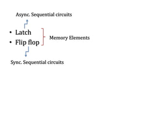
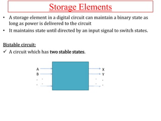
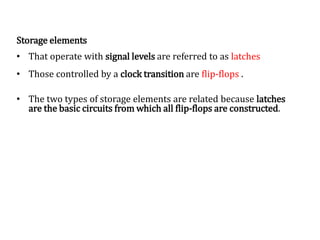
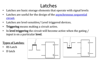
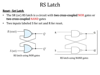
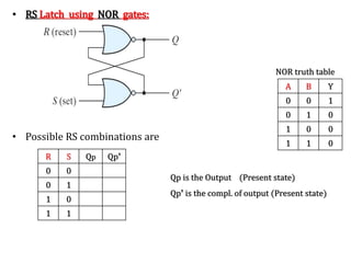

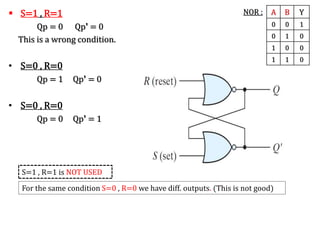
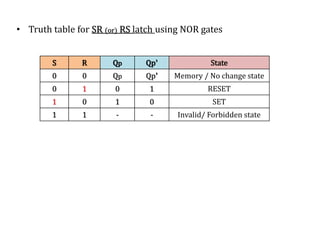
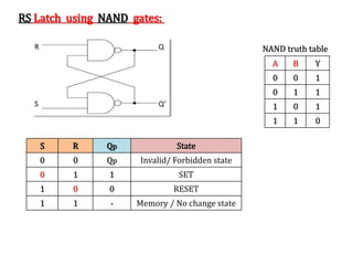


The document explains the fundamental concepts of latches and flip-flops in digital circuits, which are essential storage elements that maintain binary states. It discusses the operation of the RS latch using NOR and NAND gates, along with their input-output behaviors illustrated by truth tables. The document emphasizes the differences between latches and flip-flops, focusing on how latches are level-sensitive devices, while flip-flops are controlled by clock transitions.