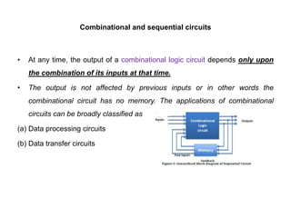
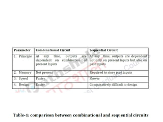
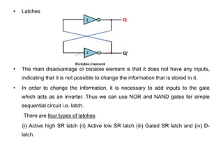
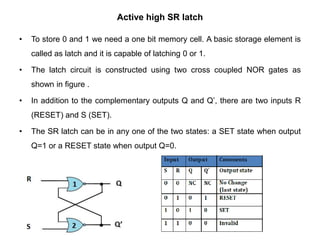
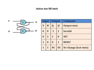
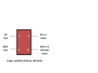
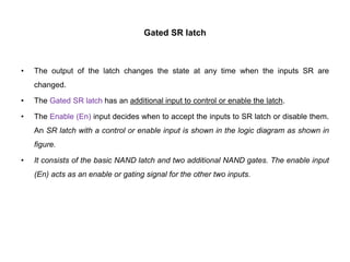
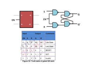
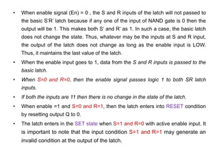
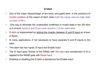
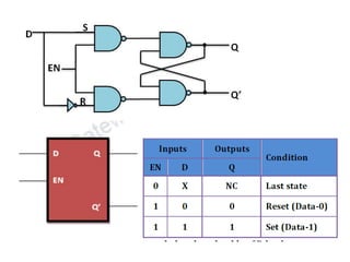
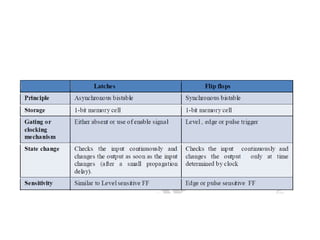
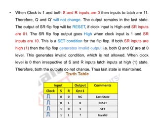
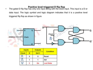
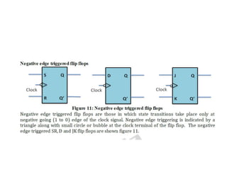
Unit IV
SYNCHRONOUS SEQUENTIAL LOGIC
Introduction
• Digital systems are mainly categorized as combinational logic circuits or
sequential logic circuits.
• All the applications of digital systems discussed so far like logic gates, adder,
subtractor,comparator, parity generator/checker, multiplexers, demultiplexers,
encoders and decoders are the examples of combinational circuits.
• Whereas there is range of logic circuits like latches, flipflops, counters and
registers are few popular applications of sequential circuits.
• The combinational logic circuit and sequential logic circuits differ mainly in the
way the outputs are obtained.
• In combinational circuits, the outputs are the function of the combination of
inputs applied at given time.
• But there are certain situations like wherein the output of the logic circuits should be
generated after the occurrence of particular sequence of inputs.
• For example in traffic light controller circuit, the Green light should be turned ON only after
RED light, or Washing machine should start wash cycle only after having sufficient water in
the tub, and so on. Such circuits are popularly known as sequential circuits.
• In sequential circuits, the output of the circuit is a function of present input as well as past
inputs.
• This indicates there is a need to some kind of memory cell to store the previous inputs.
• Latches and flip flops are basically two categories of bistable multivibrators used for storing
1-bit information.
• There are four types of latches namely
• Active low SR, Active high SR, Gated SR latch and D latch.
• Flip flops/ latches can be used as for storing information, counting events or generating a
desired sequence for various electronic systems.
Combinational and sequential circuits
• At any time, the output of a combinational logic circuit depends only upon
the combination of its inputs at that time.
• The output is not affected by previous inputs or in other words the
combinational circuit has no memory. The applications of combinational
circuits can be broadly classified as
(a) Data processing circuits
(b) Data transfer circuits
• Latches
• The main disadvantage of bistable element is that it does not have any inputs,
indicating that it is not possible to change the information that is stored in it.
• In order to change the information, it is necessary to add inputs to the gate
which acts as an inverter. Thus we can use NOR and NAND gates for simple
sequential circuit i.e. latch.
There are four types of latches
(i) Active high SR latch (ii) Active low SR latch (iii) Gated SR latch and (iv) D-
latch.
Active high SR latch
• To store 0 and 1 we need a one bit memory cell. A basic storage element is
called as latch and it is capable of latching 0 or 1.
• The latch circuit is constructed using two cross coupled NOR gates as
shown in figure .
• In addition to the complementary outputs Q and Q’, there are two inputs R
(RESET) and S (SET).
• The SR latch can be in any one of the two states: a SET state when output
Q=1 or a RESET state when output Q=0.
Active low SR latch
Gated SR latch
• The output of the latch changes the state at any time when the inputs SR are
changed.
• The Gated SR latch has an additional input to control or enable the latch.
• The Enable (En) input decides when to accept the inputs to SR latch or disable them.
An SR latch with a control or enable input is shown in the logic diagram as shown in
figure.
• It consists of the basic NAND latch and two additional NAND gates. The enable input
(En) acts as an enable or gating signal for the other two inputs.
• When enable signal (En) = 0 , the S and R inputs of the latch will not passed to
the basic S’R’ latch because if any one of the input of NAND gate is 0 then the
output will be 1. This makes both S’ and R’ as 1. In such a case, the basic latch
does not change the state. Thus, whatever may be the inputs at S and R input,
the output of the latch does not change as long as the enable input is LOW.
Thus, it maintains the last value of the latch.
• When the enable input goes to 1, data from the S and R inputs is passed to the
basic latch.
• When S=0 and R=0, then the enable signal passes logic 1 to both SR latch
inputs.
• If both the inputs are 11 then there is no change in the state of the latch.
• When enable =1 and S=0 and R=1, then the latch enters into RESET condition
by resetting output Q to 0.
• The latch enters in the SET state when S=1 and R=0 with active enable input. It
is important to note that the input condition S=1 and R=1 may generate an
invalid condition at the output of the latch.
D latch
• One of the major disadvantage of the basic and gated latch, is the presence of
invalid condition at the output of latch when both the inputs assume high state
i.e when S=R=1.
• One way to eliminate the undesirable undefined or invalid state in the SR latch
is to ensure inputs S and R are never equal to 1 at the same time.
• D latch is implemented by adding the inverter between S and R input as shown
in figure .
• In many applications, it not necessary to have separate S and R inputs to the
latch.
• This latch has two inputs: D input and Enable input.
• The D input goes directly to the NAND with Set input and complement of D is
applied to the NAND gate with Reset input.
• Enabling or disabling the D latch is decided by the Enable input.
• Let us now study the operation of gated D latch.
• If enable input is 0 i.e. data input is disabled then there is no change in the
output of latch.
• As long as the enable or gating input is 0, the basic S’R’ latch has both
inputs at the logic 1 level, and the circuit cannot change state regardless of
the value of D.
• When the enable input is 1 (High), then the data present at D input is
transferred to Q output.
• If D is 0, output Q goes to 0, providing the RESET condition of the latch.
• If D is 1, the Q output goes to 1, placing the circuit in the set state.
• In other word, we can say that the output Q follows the D input when enable
input is high.
• Therefore, this latch is also called as transparent data or D latch.
Comparison between latches and Flip flops
• Latches and flip flops are sequential circuits capable of storing an information
and find applications in many electronic gadgets.
• Figure-1 indicates the comparison table for latches and flip flops. First column in
the table includes important keywords or parameters used for the comparison.
• Latches are asynchronous bistable multivibrator devices whereas flip flops are
synchronous bistable multivibrator devices.
• Latches and flip flops are the basic elements and these are used to store
information. One flip flop and latch can store one bit of data, hence referred to
as 1-bit memory cell. Latch can hold the data without gating or clocking signal.
Certain latches can use enable signal for gating the data into the latch. It
changes state whenever the enable is asserted. Flip flops can store the data in
synchronism with a clock signal. Flip flops can be clocked as level, edge or
pulse triggering methods.
Positive level triggered SR flip flop
• The logic symbol of SR flip contains two SR inputs, a clock input and
complementary outputs Q and Q’ is shown in figure.
• The logic diagram contains two sections: Gating circuit for latch with clock
input and an active low cross coupled NAND latch.
• When clock input is at High level (1), S and R inputs controls the state of
latch.
• When Clock is 1 and both S and R inputs are 0 then inputs to latch are 11.
Therefore, Q and Q’ will not change. The output remains in the last state.
The output of SR flip flop will be RESET, if clock input is High and SR inputs
are 01. The SR flip flop output goes High when clock input is 1 and SR
inputs are 10. This is a SET condition for the flip flop. If both SR inputs are
high (1) then the flip flop generates invalid output i.e. both Q and Q’ are at 0
level. This generates invalid condition, which is not allowed. When clock
level is 0 then irrespective of S and R inputs latch inputs at high (1) state.
Therefore, both the outputs do not change. Thus last state is maintained.
Positive level triggered D flip flop
• The gated D flip flop has only one input along with the clock input. This input is a D or
data input. The logic symbol and logic diagram indicates that it is a positive level
triggered flip flop as shown in figure
• When the clock input is high, the Q output follows the input D. It is possible
to store data 0 or 1 in the flip flop.
• When D=0 then flip flop output is RESET state and at D=1, the flip flops
stores 1 i.e. SET state.
• During low level of clock irrespective of the value of D input, the Q output of
flip flop do not change irrespective of D input.
• Thus flip flop keeps the last state.
• As the inputs appear at output after some delay, hence D flip flop is also
called as Delay flip flop
Positive level triggered JK flip flop
• The basic SR flip circuit has many applications but it has some switching problems. First,
when both S and R input are at logic 1 then SR flip flop generate invalid or not allowed
condition, which must always be avoided.
• Similarly, if S or R input changes when clock is active then the correct latching action may
not occur.
• To overcome these two problems with SR flip flop, the JK flip flop is developed.
• The JK flip flop is considered to be a universal flip flop because it is possible to convert JK
flip flop into any other types of flip flops like SR or D type.
• The logic symbol of this flip flop includes JK inputs along with Clock input.
• The JK flip flop is exactly the same as the SR flip flop except the difference is that it does
not generate invalid or not allowed condition.
• The logic diagram of flip flop indicates that both S and R inputs of SR flip flop are replaced
by two inputs called the J and K inputs respectively i.e. J=S and K=R.
• The name JK flip flop is given after its inventor Jack Kilby.
Race-around condition
• The unpredictable or invalid condition of SR flip flop when both inputs are
1(S=R=1) is eliminated in a JK flip flop by using the feedback connection from
outputs to the inputs. Therefore, changes in the output results change in input.
• Consider for example that the inputs J=K=1 and CLK=1. Let us assume Q=0.
After a time t equal to propagation delay through two NAND gates in series the
output will change to Q=1. Now we have J=K=1 and Q=1 and after another time
t the output will change back to Q=0. Hence , we conclude that as long as
CLK=1, the outputs will oscillate back and forth between 0 and 1. At the end of
clock the output Q value is uncertain.
• This situation is referred to as the race around condition.
• To avoid racing, it is now important to think about different approach in designing
the flip flop.
Master Slave JK flip flop
• There are basically two sections – master section and slave section. The
external control inputs (i.e. J, K and Clock) are applied to master JK section.
The slave section is the same as the master section except that it is clocked
on inverted clock pulse and is controlled by the outputs of the master section.
• The feedbacks from slave Q and Q’ are connected to master JK inputs. The
master section assumes the state determined by the J and K inputs at the
positive going edge of the clock pulse and the slave section at the negative
going edge of the clock pulse. The state of the slave then immediately
appears at Q and Q’ outputs. Q output of slave is connected back to NAND
gate which receives K input of master and Q’ output is connected back into
NAND gate which receives J input of master.
• When J=0 and K=0 at pulse triggering, there is no change at the output of
the flip flop. In short, the flip flop holds the last state. When J=0 and K=1 at
pulse trigger, the flip flop enters in Reset state i.e. Q=0. Flip flop enters into
SET state, when J=1 and K=0 at pulse clock transition. When J=1 and K=1
at triggering transition, the flip flop toggles i.e. goes to the complement of
the present state. Note that, in this pulse triggering method, the flip flop
changes the state only once after a clock pulse. Thus the problem of racing
is avoided.

Unit IV version I.ppt

  • 1.
  • 2.
    Introduction • Digital systemsare mainly categorized as combinational logic circuits or sequential logic circuits. • All the applications of digital systems discussed so far like logic gates, adder, subtractor,comparator, parity generator/checker, multiplexers, demultiplexers, encoders and decoders are the examples of combinational circuits. • Whereas there is range of logic circuits like latches, flipflops, counters and registers are few popular applications of sequential circuits. • The combinational logic circuit and sequential logic circuits differ mainly in the way the outputs are obtained. • In combinational circuits, the outputs are the function of the combination of inputs applied at given time.
  • 3.
    • But thereare certain situations like wherein the output of the logic circuits should be generated after the occurrence of particular sequence of inputs. • For example in traffic light controller circuit, the Green light should be turned ON only after RED light, or Washing machine should start wash cycle only after having sufficient water in the tub, and so on. Such circuits are popularly known as sequential circuits. • In sequential circuits, the output of the circuit is a function of present input as well as past inputs. • This indicates there is a need to some kind of memory cell to store the previous inputs. • Latches and flip flops are basically two categories of bistable multivibrators used for storing 1-bit information. • There are four types of latches namely • Active low SR, Active high SR, Gated SR latch and D latch. • Flip flops/ latches can be used as for storing information, counting events or generating a desired sequence for various electronic systems.
  • 4.
    Combinational and sequentialcircuits • At any time, the output of a combinational logic circuit depends only upon the combination of its inputs at that time. • The output is not affected by previous inputs or in other words the combinational circuit has no memory. The applications of combinational circuits can be broadly classified as (a) Data processing circuits (b) Data transfer circuits
  • 6.
    • Latches • Themain disadvantage of bistable element is that it does not have any inputs, indicating that it is not possible to change the information that is stored in it. • In order to change the information, it is necessary to add inputs to the gate which acts as an inverter. Thus we can use NOR and NAND gates for simple sequential circuit i.e. latch. There are four types of latches (i) Active high SR latch (ii) Active low SR latch (iii) Gated SR latch and (iv) D- latch.
  • 7.
    Active high SRlatch • To store 0 and 1 we need a one bit memory cell. A basic storage element is called as latch and it is capable of latching 0 or 1. • The latch circuit is constructed using two cross coupled NOR gates as shown in figure . • In addition to the complementary outputs Q and Q’, there are two inputs R (RESET) and S (SET). • The SR latch can be in any one of the two states: a SET state when output Q=1 or a RESET state when output Q=0.
  • 8.
  • 10.
    Gated SR latch •The output of the latch changes the state at any time when the inputs SR are changed. • The Gated SR latch has an additional input to control or enable the latch. • The Enable (En) input decides when to accept the inputs to SR latch or disable them. An SR latch with a control or enable input is shown in the logic diagram as shown in figure. • It consists of the basic NAND latch and two additional NAND gates. The enable input (En) acts as an enable or gating signal for the other two inputs.
  • 12.
    • When enablesignal (En) = 0 , the S and R inputs of the latch will not passed to the basic S’R’ latch because if any one of the input of NAND gate is 0 then the output will be 1. This makes both S’ and R’ as 1. In such a case, the basic latch does not change the state. Thus, whatever may be the inputs at S and R input, the output of the latch does not change as long as the enable input is LOW. Thus, it maintains the last value of the latch. • When the enable input goes to 1, data from the S and R inputs is passed to the basic latch. • When S=0 and R=0, then the enable signal passes logic 1 to both SR latch inputs. • If both the inputs are 11 then there is no change in the state of the latch. • When enable =1 and S=0 and R=1, then the latch enters into RESET condition by resetting output Q to 0. • The latch enters in the SET state when S=1 and R=0 with active enable input. It is important to note that the input condition S=1 and R=1 may generate an invalid condition at the output of the latch.
  • 13.
    D latch • Oneof the major disadvantage of the basic and gated latch, is the presence of invalid condition at the output of latch when both the inputs assume high state i.e when S=R=1. • One way to eliminate the undesirable undefined or invalid state in the SR latch is to ensure inputs S and R are never equal to 1 at the same time. • D latch is implemented by adding the inverter between S and R input as shown in figure . • In many applications, it not necessary to have separate S and R inputs to the latch. • This latch has two inputs: D input and Enable input. • The D input goes directly to the NAND with Set input and complement of D is applied to the NAND gate with Reset input. • Enabling or disabling the D latch is decided by the Enable input.
  • 15.
    • Let usnow study the operation of gated D latch. • If enable input is 0 i.e. data input is disabled then there is no change in the output of latch. • As long as the enable or gating input is 0, the basic S’R’ latch has both inputs at the logic 1 level, and the circuit cannot change state regardless of the value of D. • When the enable input is 1 (High), then the data present at D input is transferred to Q output. • If D is 0, output Q goes to 0, providing the RESET condition of the latch. • If D is 1, the Q output goes to 1, placing the circuit in the set state. • In other word, we can say that the output Q follows the D input when enable input is high. • Therefore, this latch is also called as transparent data or D latch.
  • 16.
    Comparison between latchesand Flip flops • Latches and flip flops are sequential circuits capable of storing an information and find applications in many electronic gadgets. • Figure-1 indicates the comparison table for latches and flip flops. First column in the table includes important keywords or parameters used for the comparison. • Latches are asynchronous bistable multivibrator devices whereas flip flops are synchronous bistable multivibrator devices. • Latches and flip flops are the basic elements and these are used to store information. One flip flop and latch can store one bit of data, hence referred to as 1-bit memory cell. Latch can hold the data without gating or clocking signal. Certain latches can use enable signal for gating the data into the latch. It changes state whenever the enable is asserted. Flip flops can store the data in synchronism with a clock signal. Flip flops can be clocked as level, edge or pulse triggering methods.
  • 19.
    Positive level triggeredSR flip flop • The logic symbol of SR flip contains two SR inputs, a clock input and complementary outputs Q and Q’ is shown in figure. • The logic diagram contains two sections: Gating circuit for latch with clock input and an active low cross coupled NAND latch. • When clock input is at High level (1), S and R inputs controls the state of latch.
  • 20.
    • When Clockis 1 and both S and R inputs are 0 then inputs to latch are 11. Therefore, Q and Q’ will not change. The output remains in the last state. The output of SR flip flop will be RESET, if clock input is High and SR inputs are 01. The SR flip flop output goes High when clock input is 1 and SR inputs are 10. This is a SET condition for the flip flop. If both SR inputs are high (1) then the flip flop generates invalid output i.e. both Q and Q’ are at 0 level. This generates invalid condition, which is not allowed. When clock level is 0 then irrespective of S and R inputs latch inputs at high (1) state. Therefore, both the outputs do not change. Thus last state is maintained.
  • 21.
    Positive level triggeredD flip flop • The gated D flip flop has only one input along with the clock input. This input is a D or data input. The logic symbol and logic diagram indicates that it is a positive level triggered flip flop as shown in figure
  • 22.
    • When theclock input is high, the Q output follows the input D. It is possible to store data 0 or 1 in the flip flop. • When D=0 then flip flop output is RESET state and at D=1, the flip flops stores 1 i.e. SET state. • During low level of clock irrespective of the value of D input, the Q output of flip flop do not change irrespective of D input. • Thus flip flop keeps the last state. • As the inputs appear at output after some delay, hence D flip flop is also called as Delay flip flop
  • 23.
    Positive level triggeredJK flip flop • The basic SR flip circuit has many applications but it has some switching problems. First, when both S and R input are at logic 1 then SR flip flop generate invalid or not allowed condition, which must always be avoided. • Similarly, if S or R input changes when clock is active then the correct latching action may not occur. • To overcome these two problems with SR flip flop, the JK flip flop is developed. • The JK flip flop is considered to be a universal flip flop because it is possible to convert JK flip flop into any other types of flip flops like SR or D type. • The logic symbol of this flip flop includes JK inputs along with Clock input. • The JK flip flop is exactly the same as the SR flip flop except the difference is that it does not generate invalid or not allowed condition. • The logic diagram of flip flop indicates that both S and R inputs of SR flip flop are replaced by two inputs called the J and K inputs respectively i.e. J=S and K=R. • The name JK flip flop is given after its inventor Jack Kilby.
  • 25.
    Race-around condition • Theunpredictable or invalid condition of SR flip flop when both inputs are 1(S=R=1) is eliminated in a JK flip flop by using the feedback connection from outputs to the inputs. Therefore, changes in the output results change in input. • Consider for example that the inputs J=K=1 and CLK=1. Let us assume Q=0. After a time t equal to propagation delay through two NAND gates in series the output will change to Q=1. Now we have J=K=1 and Q=1 and after another time t the output will change back to Q=0. Hence , we conclude that as long as CLK=1, the outputs will oscillate back and forth between 0 and 1. At the end of clock the output Q value is uncertain. • This situation is referred to as the race around condition. • To avoid racing, it is now important to think about different approach in designing the flip flop.
  • 29.
    Master Slave JKflip flop • There are basically two sections – master section and slave section. The external control inputs (i.e. J, K and Clock) are applied to master JK section. The slave section is the same as the master section except that it is clocked on inverted clock pulse and is controlled by the outputs of the master section. • The feedbacks from slave Q and Q’ are connected to master JK inputs. The master section assumes the state determined by the J and K inputs at the positive going edge of the clock pulse and the slave section at the negative going edge of the clock pulse. The state of the slave then immediately appears at Q and Q’ outputs. Q output of slave is connected back to NAND gate which receives K input of master and Q’ output is connected back into NAND gate which receives J input of master.
  • 31.
    • When J=0and K=0 at pulse triggering, there is no change at the output of the flip flop. In short, the flip flop holds the last state. When J=0 and K=1 at pulse trigger, the flip flop enters in Reset state i.e. Q=0. Flip flop enters into SET state, when J=1 and K=0 at pulse clock transition. When J=1 and K=1 at triggering transition, the flip flop toggles i.e. goes to the complement of the present state. Note that, in this pulse triggering method, the flip flop changes the state only once after a clock pulse. Thus the problem of racing is avoided.

Editor's Notes

  • #27 The problem of race around condition in the level triggered flip flop can be solved by ‘edge triggering’ the flip flop. Flip flops change state either at the positive edge (rising edge) or at the negative edge (falling) edge of the clock pulse as shown in figure 9.. These are also called as Low-to-high or High-to-low clock transitions.