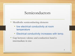
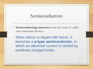
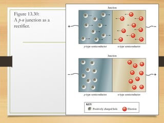
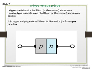
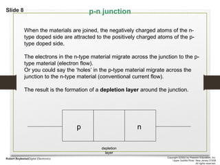
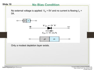
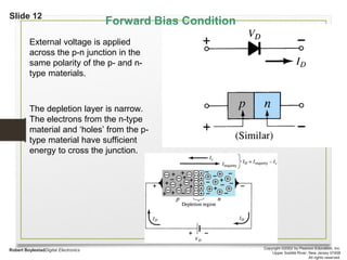
SlideShare a Scribd company logo
Solids: Conductors, Insulators and
Semiconductors
• Conductors: mostly metals
• Insulators: mostly nonmetal materials
• we’ll study allotropes of carbon and study their
properties
• Semiconductors: metalloids
1
Solids: Conductors, Insulators and
Semiconductors
2
Conductor Insulator Semiconductor
Valence Band
in red
Conduction Band: white
Band gap
No gap
Solids: Conductors, Insulators and
Semiconductors
3
Conductor Insulator
Band gap = 5.5 eV
≈ 530 kJ/mol
No gap
Graphite
Diamond
Solids: Conductors, Insulators and
Semiconductors
4
Semiconductor
Band gap
Band Gap for Semiconductors
Diamond 5.5 eV
Si 1.1 eV
Ge 0.67 eV
Semiconductors
• Metalloids: semiconducting elements
• low electrical conductivity at room
temperature
• Electrical conductivity increases with temp.
• Gap between valence and conduction band is
intermediate in size
5
Semiconductors
• Semiconducting elements form the basis of solid
state electronic devices.
6
– A striking property of these elements is that their
conductivities increase markedly when they are
doped with small quantities of other elements.
– Metalloids (such as silicon or germanium) are
semiconducting elements whose electrical
conductivity increases as temperature increases.
Semiconductors
• Semiconducting elements form the basis of solid
state electronic devices.
7
– When silicon is doped with boron, it
becomes a p-type semiconductor, in
which an electrical current is carried by
positively charged holes
Semiconductors
• Semiconducting elements form the basis of solid
state electronic devices.
8
– Joining a p-type semiconductor to an n-
type semiconductor produces a p-n
junction, which can function as a rectifier.
– A rectifier is a device that allows current to
flow in one direction, but not the other.
Figure 13.30:
A p-n junction as a
rectifier.
9
Slide 5
Robert BoylestadDigital Electronics Copyright ©2002 by Pearson Education, Inc.
Upper Saddle River, New Jersey 07458
All rights reserved.
Semiconductor Materials
Common materials used in the development of semiconductor
devices:
• Silicon (Si)
• Germanium (Ge)
Slide 6
Robert BoylestadDigital Electronics Copyright ©2002 by Pearson Education, Inc.
Upper Saddle River, New Jersey 07458
All rights reserved.
Doping
The electrical characteristics of Silicon and Germanium are improved
by adding materials in a process called doping.
The additional materials are in two types:
• n-type
• p-type
Slide 7
Robert BoylestadDigital Electronics Copyright ©2002 by Pearson Education, Inc.
Upper Saddle River, New Jersey 07458
All rights reserved.
n-type materials make the Silicon (or Germanium) atoms more
negative-type materials make the Silicon (or Germanium) atoms more
positive.
Join n-type and p-type doped Silicon (or Germanium) to form a p-n
junction.
n-type versus p-type
Slide 8
Robert BoylestadDigital Electronics Copyright ©2002 by Pearson Education, Inc.
Upper Saddle River, New Jersey 07458
All rights reserved.
p-n junction
When the materials are joined, the negatively charged atoms of the n-
type doped side are attracted to the positively charged atoms of the p-
type doped side.
The electrons in the n-type material migrate across the junction to the p-
type material (electron flow).
Or you could say the ‘holes’ in the p-type material migrate across the
junction to the n-type material (conventional current flow).
The result is the formation of a depletion layer around the junction.
depletion
layer
p n
Slide 9
Robert BoylestadDigital Electronics Copyright ©2002 by Pearson Education, Inc.
Upper Saddle River, New Jersey 07458
All rights reserved.
Operating Conditions
• No Bias
• Forward Bias
• Reverse Bias
Slide 10
Robert BoylestadDigital Electronics Copyright ©2002 by Pearson Education, Inc.
Upper Saddle River, New Jersey 07458
All rights reserved.
No external voltage is applied: VD = 0V and no current is flowing ID =
0A.
Only a modest depletion layer exists.
No Bias Condition
Slide 11
Robert BoylestadDigital Electronics Copyright ©2002 by Pearson Education, Inc.
Upper Saddle River, New Jersey 07458
All rights reserved.
Reverse Bias Condition
External voltage is applied across the p-n junction
in the opposite polarity of the p- and n-type materials.
This causes the depletion layer to widen.
The electrons in the n-type material are attracted
towards the positive terminal and the ‘holes’ in
the p-type material are attracted towards the
negative terminal.
Slide 12
Robert BoylestadDigital Electronics Copyright ©2002 by Pearson Education, Inc.
Upper Saddle River, New Jersey 07458
All rights reserved.
Forward Bias Condition
External voltage is applied
across the p-n junction in the
same polarity of the p- and n-
type materials.
The depletion layer is narrow.
The electrons from the n-type
material and ‘holes’ from the p-
type material have sufficient
energy to cross the junction.
Slide 28
Robert BoylestadDigital Electronics Copyright ©2002 by Pearson Education, Inc.
Upper Saddle River, New Jersey 07458
All rights reserved.
An ohmmeter set on a low ohm's scale can be used to test a diode.
A normal diode will have the following readings.
The diode should be tested out of circuit.
B. Ohmmeter
Slide 30
Robert BoylestadDigital Electronics Copyright ©2002 by Pearson Education, Inc.
Upper Saddle River, New Jersey 07458
All rights reserved.
Other Types of Diodes
1. Zener Diode2. Light Emitting Diode
3. Diode Arrays
Slide 31
Robert BoylestadDigital Electronics Copyright ©2002 by Pearson Education, Inc.
Upper Saddle River, New Jersey 07458
All rights reserved.
A Zener is a diode operated in reverse bias at the Peak Inverse Voltage (PIV)
called the Zener Voltage (VZ).
Symbol
Common Zener Voltages: 1.8V to 200V
1. Zener Diode
Slide 32
Robert BoylestadDigital Electronics Copyright ©2002 by Pearson Education, Inc.
Upper Saddle River, New Jersey 07458
All rights reserved.
2. Light Emitting Diode (LED)
This diode when forward biased emits photons. These can be in the visible
spectrum.
Symbol
The forward bias voltage is higher, usually around 2-3V.
Slide 33
Robert BoylestadDigital Electronics Copyright ©2002 by Pearson Education, Inc.
Upper Saddle River, New Jersey 07458
All rights reserved.
Multiple diodes can be packaged together in an integrated circuit (IC).
A variety of combinations exist.
Example of an array:
3. Diode Arrays

More Related Content

Similar to chap.1.pdf

Semiconductor devices
Semiconductor devicesSemiconductor devices
Semiconductor devices
GS Virdi
 
Electronic devices-and-circuit-theory-10th-ed-boylestad-chapter-1
Electronic devices-and-circuit-theory-10th-ed-boylestad-chapter-1Electronic devices-and-circuit-theory-10th-ed-boylestad-chapter-1
Electronic devices-and-circuit-theory-10th-ed-boylestad-chapter-1Shiwam Isrie
 
ELECTRONIC DEVICES
ELECTRONIC DEVICESELECTRONIC DEVICES
ELECTRONIC DEVICES
ssuserb29892
 
Chapter 38
Chapter 38Chapter 38
Chapter 38mcfalltj
 
Diodes and rectifiers
Diodes and rectifiersDiodes and rectifiers
Diodes and rectifiers
Ankit Dubey
 
BASIC ELECTRONICS on physics for teaching grade 12
BASIC ELECTRONICS on physics for teaching grade 12BASIC ELECTRONICS on physics for teaching grade 12
BASIC ELECTRONICS on physics for teaching grade 12
JerryOgugo
 
DHRUV PHYSICS PPT.pptx
DHRUV PHYSICS  PPT.pptxDHRUV PHYSICS  PPT.pptx
DHRUV PHYSICS PPT.pptx
SaiKumar761648
 
7760402.ppt
7760402.ppt7760402.ppt
7760402.ppt
MilkTea45
 
Physics of LEDs
Physics of LEDsPhysics of LEDs
Physics of LEDsTan Kim
 
Semiconductor Diode: Introduction and Application
Semiconductor Diode: Introduction and ApplicationSemiconductor Diode: Introduction and Application
Semiconductor Diode: Introduction and Application
Samir Raj Bhandari
 
Semiconductor and It's Importance
Semiconductor and It's ImportanceSemiconductor and It's Importance
Semiconductor and It's Importance
Paurav Shah
 
Bem (3)
Bem (3)Bem (3)
EDC ( P-type & N-type )
EDC ( P-type & N-type )EDC ( P-type & N-type )
EDC ( P-type & N-type )
Pritam Shil
 
MS4SSA-IntroductiontoSemiconductors.ppt
MS4SSA-IntroductiontoSemiconductors.pptMS4SSA-IntroductiontoSemiconductors.ppt
MS4SSA-IntroductiontoSemiconductors.ppt
NagaKiran Kumar
 
MS4SSA-.pptfeetrererertryrtrtererwewwwew
MS4SSA-.pptfeetrererertryrtrtererwewwwewMS4SSA-.pptfeetrererertryrtrtererwewwwew
MS4SSA-.pptfeetrererertryrtrtererwewwwew
SoniaChebouki
 
Importance of Semiconductorits.pptx
Importance of Semiconductorits.pptxImportance of Semiconductorits.pptx
Importance of Semiconductorits.pptx
Amanda153361
 
Blue light Emitting Diode
Blue light Emitting Diode Blue light Emitting Diode
Blue light Emitting Diode
Mohamed Hasanin
 
DOC-20221018-WA0001..pptx
DOC-20221018-WA0001..pptxDOC-20221018-WA0001..pptx
DOC-20221018-WA0001..pptx
PVenkataGaneshReddy
 

Similar to chap.1.pdf (20)

Semiconductor devices
Semiconductor devicesSemiconductor devices
Semiconductor devices
 
Electronic devices-and-circuit-theory-10th-ed-boylestad-chapter-1
Electronic devices-and-circuit-theory-10th-ed-boylestad-chapter-1Electronic devices-and-circuit-theory-10th-ed-boylestad-chapter-1
Electronic devices-and-circuit-theory-10th-ed-boylestad-chapter-1
 
ELECTRONIC DEVICES
ELECTRONIC DEVICESELECTRONIC DEVICES
ELECTRONIC DEVICES
 
Chapter 38
Chapter 38Chapter 38
Chapter 38
 
Diodes and rectifiers
Diodes and rectifiersDiodes and rectifiers
Diodes and rectifiers
 
Ch01
Ch01Ch01
Ch01
 
BASIC ELECTRONICS on physics for teaching grade 12
BASIC ELECTRONICS on physics for teaching grade 12BASIC ELECTRONICS on physics for teaching grade 12
BASIC ELECTRONICS on physics for teaching grade 12
 
DHRUV PHYSICS PPT.pptx
DHRUV PHYSICS  PPT.pptxDHRUV PHYSICS  PPT.pptx
DHRUV PHYSICS PPT.pptx
 
7760402.ppt
7760402.ppt7760402.ppt
7760402.ppt
 
Physics of LEDs
Physics of LEDsPhysics of LEDs
Physics of LEDs
 
Semiconductor Diode: Introduction and Application
Semiconductor Diode: Introduction and ApplicationSemiconductor Diode: Introduction and Application
Semiconductor Diode: Introduction and Application
 
Semiconductordevices
SemiconductordevicesSemiconductordevices
Semiconductordevices
 
Semiconductor and It's Importance
Semiconductor and It's ImportanceSemiconductor and It's Importance
Semiconductor and It's Importance
 
Bem (3)
Bem (3)Bem (3)
Bem (3)
 
EDC ( P-type & N-type )
EDC ( P-type & N-type )EDC ( P-type & N-type )
EDC ( P-type & N-type )
 
MS4SSA-IntroductiontoSemiconductors.ppt
MS4SSA-IntroductiontoSemiconductors.pptMS4SSA-IntroductiontoSemiconductors.ppt
MS4SSA-IntroductiontoSemiconductors.ppt
 
MS4SSA-.pptfeetrererertryrtrtererwewwwew
MS4SSA-.pptfeetrererertryrtrtererwewwwewMS4SSA-.pptfeetrererertryrtrtererwewwwew
MS4SSA-.pptfeetrererertryrtrtererwewwwew
 
Importance of Semiconductorits.pptx
Importance of Semiconductorits.pptxImportance of Semiconductorits.pptx
Importance of Semiconductorits.pptx
 
Blue light Emitting Diode
Blue light Emitting Diode Blue light Emitting Diode
Blue light Emitting Diode
 
DOC-20221018-WA0001..pptx
DOC-20221018-WA0001..pptxDOC-20221018-WA0001..pptx
DOC-20221018-WA0001..pptx
 

Recently uploaded

Smart TV Buyer Insights Survey 2024 by 91mobiles.pdf
Smart TV Buyer Insights Survey 2024 by 91mobiles.pdfSmart TV Buyer Insights Survey 2024 by 91mobiles.pdf
Smart TV Buyer Insights Survey 2024 by 91mobiles.pdf
91mobiles
 
Assuring Contact Center Experiences for Your Customers With ThousandEyes
Assuring Contact Center Experiences for Your Customers With ThousandEyesAssuring Contact Center Experiences for Your Customers With ThousandEyes
Assuring Contact Center Experiences for Your Customers With ThousandEyes
ThousandEyes
 
Empowering NextGen Mobility via Large Action Model Infrastructure (LAMI): pav...
Empowering NextGen Mobility via Large Action Model Infrastructure (LAMI): pav...Empowering NextGen Mobility via Large Action Model Infrastructure (LAMI): pav...
Empowering NextGen Mobility via Large Action Model Infrastructure (LAMI): pav...
Thierry Lestable
 
AI for Every Business: Unlocking Your Product's Universal Potential by VP of ...
AI for Every Business: Unlocking Your Product's Universal Potential by VP of ...AI for Every Business: Unlocking Your Product's Universal Potential by VP of ...
AI for Every Business: Unlocking Your Product's Universal Potential by VP of ...
Product School
 
To Graph or Not to Graph Knowledge Graph Architectures and LLMs
To Graph or Not to Graph Knowledge Graph Architectures and LLMsTo Graph or Not to Graph Knowledge Graph Architectures and LLMs
To Graph or Not to Graph Knowledge Graph Architectures and LLMs
Paul Groth
 
Epistemic Interaction - tuning interfaces to provide information for AI support
Epistemic Interaction - tuning interfaces to provide information for AI supportEpistemic Interaction - tuning interfaces to provide information for AI support
Epistemic Interaction - tuning interfaces to provide information for AI support
Alan Dix
 
Bits & Pixels using AI for Good.........
Bits & Pixels using AI for Good.........Bits & Pixels using AI for Good.........
Bits & Pixels using AI for Good.........
Alison B. Lowndes
 
Kubernetes & AI - Beauty and the Beast !?! @KCD Istanbul 2024
Kubernetes & AI - Beauty and the Beast !?! @KCD Istanbul 2024Kubernetes & AI - Beauty and the Beast !?! @KCD Istanbul 2024
Kubernetes & AI - Beauty and the Beast !?! @KCD Istanbul 2024
Tobias Schneck
 
State of ICS and IoT Cyber Threat Landscape Report 2024 preview
State of ICS and IoT Cyber Threat Landscape Report 2024 previewState of ICS and IoT Cyber Threat Landscape Report 2024 preview
State of ICS and IoT Cyber Threat Landscape Report 2024 preview
Prayukth K V
 
Monitoring Java Application Security with JDK Tools and JFR Events
Monitoring Java Application Security with JDK Tools and JFR EventsMonitoring Java Application Security with JDK Tools and JFR Events
Monitoring Java Application Security with JDK Tools and JFR Events
Ana-Maria Mihalceanu
 
Generating a custom Ruby SDK for your web service or Rails API using Smithy
Generating a custom Ruby SDK for your web service or Rails API using SmithyGenerating a custom Ruby SDK for your web service or Rails API using Smithy
Generating a custom Ruby SDK for your web service or Rails API using Smithy
g2nightmarescribd
 
PCI PIN Basics Webinar from the Controlcase Team
PCI PIN Basics Webinar from the Controlcase TeamPCI PIN Basics Webinar from the Controlcase Team
PCI PIN Basics Webinar from the Controlcase Team
ControlCase
 
FIDO Alliance Osaka Seminar: FIDO Security Aspects.pdf
FIDO Alliance Osaka Seminar: FIDO Security Aspects.pdfFIDO Alliance Osaka Seminar: FIDO Security Aspects.pdf
FIDO Alliance Osaka Seminar: FIDO Security Aspects.pdf
FIDO Alliance
 
GenAISummit 2024 May 28 Sri Ambati Keynote: AGI Belongs to The Community in O...
GenAISummit 2024 May 28 Sri Ambati Keynote: AGI Belongs to The Community in O...GenAISummit 2024 May 28 Sri Ambati Keynote: AGI Belongs to The Community in O...
GenAISummit 2024 May 28 Sri Ambati Keynote: AGI Belongs to The Community in O...
Sri Ambati
 
Essentials of Automations: Optimizing FME Workflows with Parameters
Essentials of Automations: Optimizing FME Workflows with ParametersEssentials of Automations: Optimizing FME Workflows with Parameters
Essentials of Automations: Optimizing FME Workflows with Parameters
Safe Software
 
Key Trends Shaping the Future of Infrastructure.pdf
Key Trends Shaping the Future of Infrastructure.pdfKey Trends Shaping the Future of Infrastructure.pdf
Key Trends Shaping the Future of Infrastructure.pdf
Cheryl Hung
 
The Art of the Pitch: WordPress Relationships and Sales
The Art of the Pitch: WordPress Relationships and SalesThe Art of the Pitch: WordPress Relationships and Sales
The Art of the Pitch: WordPress Relationships and Sales
Laura Byrne
 
Unsubscribed: Combat Subscription Fatigue With a Membership Mentality by Head...
Unsubscribed: Combat Subscription Fatigue With a Membership Mentality by Head...Unsubscribed: Combat Subscription Fatigue With a Membership Mentality by Head...
Unsubscribed: Combat Subscription Fatigue With a Membership Mentality by Head...
Product School
 
From Siloed Products to Connected Ecosystem: Building a Sustainable and Scala...
From Siloed Products to Connected Ecosystem: Building a Sustainable and Scala...From Siloed Products to Connected Ecosystem: Building a Sustainable and Scala...
From Siloed Products to Connected Ecosystem: Building a Sustainable and Scala...
Product School
 
De-mystifying Zero to One: Design Informed Techniques for Greenfield Innovati...
De-mystifying Zero to One: Design Informed Techniques for Greenfield Innovati...De-mystifying Zero to One: Design Informed Techniques for Greenfield Innovati...
De-mystifying Zero to One: Design Informed Techniques for Greenfield Innovati...
Product School
 

Recently uploaded (20)

Smart TV Buyer Insights Survey 2024 by 91mobiles.pdf
Smart TV Buyer Insights Survey 2024 by 91mobiles.pdfSmart TV Buyer Insights Survey 2024 by 91mobiles.pdf
Smart TV Buyer Insights Survey 2024 by 91mobiles.pdf
 
Assuring Contact Center Experiences for Your Customers With ThousandEyes
Assuring Contact Center Experiences for Your Customers With ThousandEyesAssuring Contact Center Experiences for Your Customers With ThousandEyes
Assuring Contact Center Experiences for Your Customers With ThousandEyes
 
Empowering NextGen Mobility via Large Action Model Infrastructure (LAMI): pav...
Empowering NextGen Mobility via Large Action Model Infrastructure (LAMI): pav...Empowering NextGen Mobility via Large Action Model Infrastructure (LAMI): pav...
Empowering NextGen Mobility via Large Action Model Infrastructure (LAMI): pav...
 
AI for Every Business: Unlocking Your Product's Universal Potential by VP of ...
AI for Every Business: Unlocking Your Product's Universal Potential by VP of ...AI for Every Business: Unlocking Your Product's Universal Potential by VP of ...
AI for Every Business: Unlocking Your Product's Universal Potential by VP of ...
 
To Graph or Not to Graph Knowledge Graph Architectures and LLMs
To Graph or Not to Graph Knowledge Graph Architectures and LLMsTo Graph or Not to Graph Knowledge Graph Architectures and LLMs
To Graph or Not to Graph Knowledge Graph Architectures and LLMs
 
Epistemic Interaction - tuning interfaces to provide information for AI support
Epistemic Interaction - tuning interfaces to provide information for AI supportEpistemic Interaction - tuning interfaces to provide information for AI support
Epistemic Interaction - tuning interfaces to provide information for AI support
 
Bits & Pixels using AI for Good.........
Bits & Pixels using AI for Good.........Bits & Pixels using AI for Good.........
Bits & Pixels using AI for Good.........
 
Kubernetes & AI - Beauty and the Beast !?! @KCD Istanbul 2024
Kubernetes & AI - Beauty and the Beast !?! @KCD Istanbul 2024Kubernetes & AI - Beauty and the Beast !?! @KCD Istanbul 2024
Kubernetes & AI - Beauty and the Beast !?! @KCD Istanbul 2024
 
State of ICS and IoT Cyber Threat Landscape Report 2024 preview
State of ICS and IoT Cyber Threat Landscape Report 2024 previewState of ICS and IoT Cyber Threat Landscape Report 2024 preview
State of ICS and IoT Cyber Threat Landscape Report 2024 preview
 
Monitoring Java Application Security with JDK Tools and JFR Events
Monitoring Java Application Security with JDK Tools and JFR EventsMonitoring Java Application Security with JDK Tools and JFR Events
Monitoring Java Application Security with JDK Tools and JFR Events
 
Generating a custom Ruby SDK for your web service or Rails API using Smithy
Generating a custom Ruby SDK for your web service or Rails API using SmithyGenerating a custom Ruby SDK for your web service or Rails API using Smithy
Generating a custom Ruby SDK for your web service or Rails API using Smithy
 
PCI PIN Basics Webinar from the Controlcase Team
PCI PIN Basics Webinar from the Controlcase TeamPCI PIN Basics Webinar from the Controlcase Team
PCI PIN Basics Webinar from the Controlcase Team
 
FIDO Alliance Osaka Seminar: FIDO Security Aspects.pdf
FIDO Alliance Osaka Seminar: FIDO Security Aspects.pdfFIDO Alliance Osaka Seminar: FIDO Security Aspects.pdf
FIDO Alliance Osaka Seminar: FIDO Security Aspects.pdf
 
GenAISummit 2024 May 28 Sri Ambati Keynote: AGI Belongs to The Community in O...
GenAISummit 2024 May 28 Sri Ambati Keynote: AGI Belongs to The Community in O...GenAISummit 2024 May 28 Sri Ambati Keynote: AGI Belongs to The Community in O...
GenAISummit 2024 May 28 Sri Ambati Keynote: AGI Belongs to The Community in O...
 
Essentials of Automations: Optimizing FME Workflows with Parameters
Essentials of Automations: Optimizing FME Workflows with ParametersEssentials of Automations: Optimizing FME Workflows with Parameters
Essentials of Automations: Optimizing FME Workflows with Parameters
 
Key Trends Shaping the Future of Infrastructure.pdf
Key Trends Shaping the Future of Infrastructure.pdfKey Trends Shaping the Future of Infrastructure.pdf
Key Trends Shaping the Future of Infrastructure.pdf
 
The Art of the Pitch: WordPress Relationships and Sales
The Art of the Pitch: WordPress Relationships and SalesThe Art of the Pitch: WordPress Relationships and Sales
The Art of the Pitch: WordPress Relationships and Sales
 
Unsubscribed: Combat Subscription Fatigue With a Membership Mentality by Head...
Unsubscribed: Combat Subscription Fatigue With a Membership Mentality by Head...Unsubscribed: Combat Subscription Fatigue With a Membership Mentality by Head...
Unsubscribed: Combat Subscription Fatigue With a Membership Mentality by Head...
 
From Siloed Products to Connected Ecosystem: Building a Sustainable and Scala...
From Siloed Products to Connected Ecosystem: Building a Sustainable and Scala...From Siloed Products to Connected Ecosystem: Building a Sustainable and Scala...
From Siloed Products to Connected Ecosystem: Building a Sustainable and Scala...
 
De-mystifying Zero to One: Design Informed Techniques for Greenfield Innovati...
De-mystifying Zero to One: Design Informed Techniques for Greenfield Innovati...De-mystifying Zero to One: Design Informed Techniques for Greenfield Innovati...
De-mystifying Zero to One: Design Informed Techniques for Greenfield Innovati...
 

chap.1.pdf

  • 1. Solids: Conductors, Insulators and Semiconductors • Conductors: mostly metals • Insulators: mostly nonmetal materials • we’ll study allotropes of carbon and study their properties • Semiconductors: metalloids 1
  • 2. Solids: Conductors, Insulators and Semiconductors 2 Conductor Insulator Semiconductor Valence Band in red Conduction Band: white Band gap No gap
  • 3. Solids: Conductors, Insulators and Semiconductors 3 Conductor Insulator Band gap = 5.5 eV ≈ 530 kJ/mol No gap Graphite Diamond
  • 4. Solids: Conductors, Insulators and Semiconductors 4 Semiconductor Band gap Band Gap for Semiconductors Diamond 5.5 eV Si 1.1 eV Ge 0.67 eV
  • 5. Semiconductors • Metalloids: semiconducting elements • low electrical conductivity at room temperature • Electrical conductivity increases with temp. • Gap between valence and conduction band is intermediate in size 5
  • 6. Semiconductors • Semiconducting elements form the basis of solid state electronic devices. 6 – A striking property of these elements is that their conductivities increase markedly when they are doped with small quantities of other elements. – Metalloids (such as silicon or germanium) are semiconducting elements whose electrical conductivity increases as temperature increases.
  • 7. Semiconductors • Semiconducting elements form the basis of solid state electronic devices. 7 – When silicon is doped with boron, it becomes a p-type semiconductor, in which an electrical current is carried by positively charged holes
  • 8. Semiconductors • Semiconducting elements form the basis of solid state electronic devices. 8 – Joining a p-type semiconductor to an n- type semiconductor produces a p-n junction, which can function as a rectifier. – A rectifier is a device that allows current to flow in one direction, but not the other.
  • 9. Figure 13.30: A p-n junction as a rectifier. 9
  • 10. Slide 5 Robert BoylestadDigital Electronics Copyright ©2002 by Pearson Education, Inc. Upper Saddle River, New Jersey 07458 All rights reserved. Semiconductor Materials Common materials used in the development of semiconductor devices: • Silicon (Si) • Germanium (Ge)
  • 11. Slide 6 Robert BoylestadDigital Electronics Copyright ©2002 by Pearson Education, Inc. Upper Saddle River, New Jersey 07458 All rights reserved. Doping The electrical characteristics of Silicon and Germanium are improved by adding materials in a process called doping. The additional materials are in two types: • n-type • p-type
  • 12. Slide 7 Robert BoylestadDigital Electronics Copyright ©2002 by Pearson Education, Inc. Upper Saddle River, New Jersey 07458 All rights reserved. n-type materials make the Silicon (or Germanium) atoms more negative-type materials make the Silicon (or Germanium) atoms more positive. Join n-type and p-type doped Silicon (or Germanium) to form a p-n junction. n-type versus p-type
  • 13. Slide 8 Robert BoylestadDigital Electronics Copyright ©2002 by Pearson Education, Inc. Upper Saddle River, New Jersey 07458 All rights reserved. p-n junction When the materials are joined, the negatively charged atoms of the n- type doped side are attracted to the positively charged atoms of the p- type doped side. The electrons in the n-type material migrate across the junction to the p- type material (electron flow). Or you could say the ‘holes’ in the p-type material migrate across the junction to the n-type material (conventional current flow). The result is the formation of a depletion layer around the junction. depletion layer p n
  • 14. Slide 9 Robert BoylestadDigital Electronics Copyright ©2002 by Pearson Education, Inc. Upper Saddle River, New Jersey 07458 All rights reserved. Operating Conditions • No Bias • Forward Bias • Reverse Bias
  • 15. Slide 10 Robert BoylestadDigital Electronics Copyright ©2002 by Pearson Education, Inc. Upper Saddle River, New Jersey 07458 All rights reserved. No external voltage is applied: VD = 0V and no current is flowing ID = 0A. Only a modest depletion layer exists. No Bias Condition
  • 16. Slide 11 Robert BoylestadDigital Electronics Copyright ©2002 by Pearson Education, Inc. Upper Saddle River, New Jersey 07458 All rights reserved. Reverse Bias Condition External voltage is applied across the p-n junction in the opposite polarity of the p- and n-type materials. This causes the depletion layer to widen. The electrons in the n-type material are attracted towards the positive terminal and the ‘holes’ in the p-type material are attracted towards the negative terminal.
  • 17. Slide 12 Robert BoylestadDigital Electronics Copyright ©2002 by Pearson Education, Inc. Upper Saddle River, New Jersey 07458 All rights reserved. Forward Bias Condition External voltage is applied across the p-n junction in the same polarity of the p- and n- type materials. The depletion layer is narrow. The electrons from the n-type material and ‘holes’ from the p- type material have sufficient energy to cross the junction.
  • 18. Slide 28 Robert BoylestadDigital Electronics Copyright ©2002 by Pearson Education, Inc. Upper Saddle River, New Jersey 07458 All rights reserved. An ohmmeter set on a low ohm's scale can be used to test a diode. A normal diode will have the following readings. The diode should be tested out of circuit. B. Ohmmeter
  • 19. Slide 30 Robert BoylestadDigital Electronics Copyright ©2002 by Pearson Education, Inc. Upper Saddle River, New Jersey 07458 All rights reserved. Other Types of Diodes 1. Zener Diode2. Light Emitting Diode 3. Diode Arrays
  • 20. Slide 31 Robert BoylestadDigital Electronics Copyright ©2002 by Pearson Education, Inc. Upper Saddle River, New Jersey 07458 All rights reserved. A Zener is a diode operated in reverse bias at the Peak Inverse Voltage (PIV) called the Zener Voltage (VZ). Symbol Common Zener Voltages: 1.8V to 200V 1. Zener Diode
  • 21. Slide 32 Robert BoylestadDigital Electronics Copyright ©2002 by Pearson Education, Inc. Upper Saddle River, New Jersey 07458 All rights reserved. 2. Light Emitting Diode (LED) This diode when forward biased emits photons. These can be in the visible spectrum. Symbol The forward bias voltage is higher, usually around 2-3V.
  • 22. Slide 33 Robert BoylestadDigital Electronics Copyright ©2002 by Pearson Education, Inc. Upper Saddle River, New Jersey 07458 All rights reserved. Multiple diodes can be packaged together in an integrated circuit (IC). A variety of combinations exist. Example of an array: 3. Diode Arrays