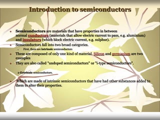
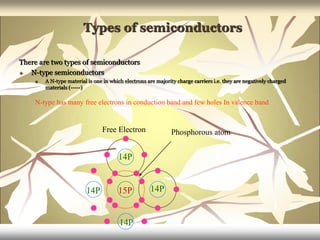
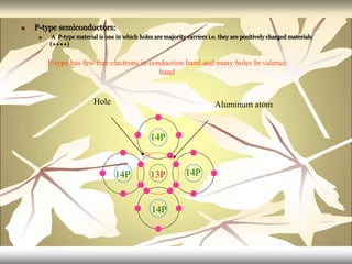
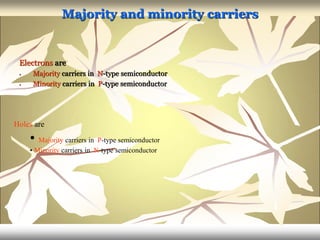
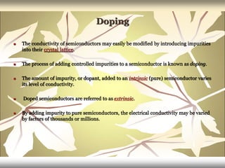
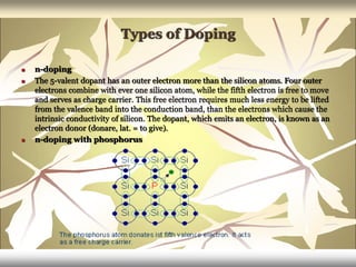
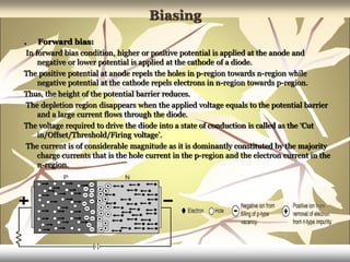
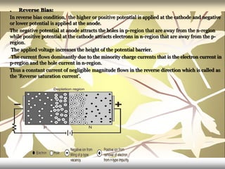
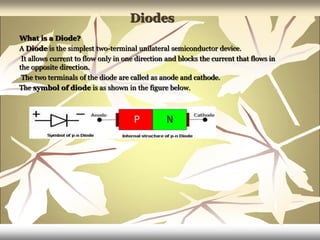
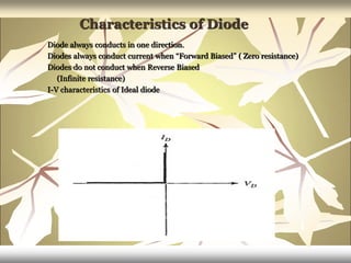
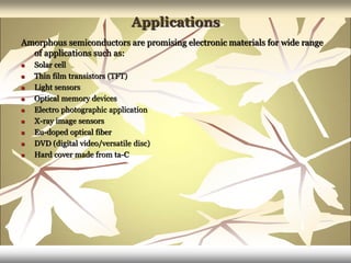
Semi-conductors
DEPARTMENT OF CHEMISTRY
SEMBODAI R.V. ARTS AND SCIENCE COLLEGE,
SEMBODAI – 614 809
Semiconductors
Overview:
Following are the topics which will be covered in this presentation.
 Introduction to semiconductors
 Types of semiconductors
 N-type semiconductors
 P-type semiconductors
 Doping
 N-type doping
 P-type doping
 Biasing
 Forward biasing
 Reverse biasing
 Diodes
 Role of semiconductors in electronics engineering
 Applications
 Importance
 Conclusion
Introduction to semiconductors
 Semiconductors are materials that have properties in between
normal conductors (materials that allow electric current to pass, e.g. aluminium)
and insulators (which block electric current, e.g. sulphur).
 Semiconductors fall into two broad categories.
1. First, there are intrinsic semiconductors
 These are composed of only one kind of material. Silicon and germanium are two
examples
 They are also called "undoped semiconductors" or "i-type semiconductors".
2-Extrinsic semiconductors.
 Which are made of intrinsic semiconductors that have had other substances added to
them to alter their properties.
Types of semiconductors
There are two types of semiconductors
 N-type semiconductors
 A N-type material is one in which electrons are majority charge carriers i.e. they are negatively charged
materials (-----)
N-type has many free electrons in conduction band and few holes In valence band
Free Electron
15P
14P
14P 14P
14P
Phosphorous atom
 P-type semiconductors:
 A P-type material is one in which holes are majority carriers i.e. they are positively charged materials
(++++)
P-type has few free electrons in conduction band and many holes In valence
band
13P
14P
14P 14P
14P
Aluminum atom
Hole
Majority and minority carriers
Electrons are
• Majority carriers in N-type semiconductor
• Minority carriers in P-type semiconductor
Holes are
• Majority carriers in P-type semiconductor
• Minority carriers in N-type semiconductor
Doping
 The conductivity of semiconductors may easily be modified by introducing impurities
into their crystal lattice.
 The process of adding controlled impurities to a semiconductor is known as doping.
 The amount of impurity, or dopant, added to an intrinsic (pure) semiconductor varies
its level of conductivity.
 Doped semiconductors are referred to as extrinsic.
 By adding impurity to pure semiconductors, the electrical conductivity may be varied
by factors of thousands or millions.
Types of Doping
 n-doping
 The 5-valent dopant has an outer electron more than the silicon atoms. Four outer
electrons combine with ever one silicon atom, while the fifth electron is free to move
and serves as charge carrier. This free electron requires much less energy to be lifted
from the valence band into the conduction band, than the electrons which cause the
intrinsic conductivity of silicon. The dopant, which emits an electron, is known as an
electron donor (donare, lat. = to give).
 n-doping with phosphorus
 P-Type doping :
 In contrast to the free electron due to doping with phosphorus, the 3-valent dopant
effect is exactly the opposite. The 3-valent dopants can catch an additional outer
electron, thus leaving a hole in the valence band of silicon atoms. Therefore the
electrons in the valence band become mobile. The holes move in the opposite
direction to the movement of the electrons. The necessary energy to lift an electron
into the energy level of indium as a dopant, is only 1 % of the energy which is needed
to raise a valence electron of silicon into the conduction band.
 p-doping with boron
Biasing
. Forward bias:
In forward bias condition, higher or positive potential is applied at the anode and
negative or lower potential is applied at the cathode of a diode.
The positive potential at anode repels the holes in p-region towards n-region while
negative potential at the cathode repels electrons in n-region towards p-region.
Thus, the height of the potential barrier reduces.
The depletion region disappears when the applied voltage equals to the potential barrier
and a large current flows through the diode.
The voltage required to drive the diode into a state of conduction is called as the ‘Cut
in/Offset/Threshold/Firing voltage’.
The current is of considerable magnitude as it is dominantly constituted by the majority
charge currents that is the hole current in the p-region and the electron current in the
n-region.
. Reverse Bias:
In reverse bias condition, the higher or positive potential is applied at the cathode and negative
or lower potential is applied at the anode.
The negative potential at anode attracts the holes in p-region that are away from the n-region
while positive potential at the cathode attracts electrons in n-region that are away from the p-
region.
The applied voltage increases the height of the potential barrier.
The current flows dominantly due to the minority charge currents that is the electron current in
p-region and the hole current in n-region.
Thus a constant current of negligible magnitude flows in the reverse direction which is called as
the ‘Reverse saturation current’.
Diodes
What is a Diode?
A Diode is the simplest two-terminal unilateral semiconductor device.
It allows current to flow only in one direction and blocks the current that flows in
the opposite direction.
The two terminals of the diode are called as anode and cathode.
The symbol of diode is as shown in the figure below.
Characteristics of Diode
Diode always conducts in one direction.
Diodes always conduct current when “Forward Biased” ( Zero resistance)
Diodes do not conduct when Reverse Biased
(Infinite resistance)
I-V characteristics of Ideal diode
I-V Characteristics of Practical Diode
Applications
Amorphous semiconductors are promising electronic materials for wide range
of applications such as:
 Solar cell
 Thin film transistors (TFT)
 Light sensors
 Optical memory devices
 Electro photographic application
 X-ray image sensors
 Eu-doped optical fiber
 DVD (digital video/versatile disc)
 Hard cover made from ta-C
Electro photographic application:
one of the most common, everyday used application is electro photography or xerography
(Greek word, meaning is “dry writing”).
The first xerography was made by Carlson and Kornei in 1938(!) in Astoria NY (USA).
The really first experiment was made using sulfur, but later on Se was the basic
material. Recently a-Si:H films have been utilized instead.
Solar cells:
Potentially the most important application of the amorphous semiconductors a-Si:H is in
the direct conversion of sunlight to electric power.
This is a cheaper raw material than crystalline silicon. No structural damage!
For example: space shuttle use.
 The conversation of solar light to electric power is available renewaable sources of
energies.
 The basic physical principle involved is the absorption of photon resulting in the
creation of electron-hole pairs; the excess electrons in the conduction band, and holes
in the valence band.
 Internal junction field separates them before recombination.
THE
END
THANK
YOU
ANY QUESTION

01 SEMI CONDUCTOR.ppt.....................

  • 1.
    Semi-conductors DEPARTMENT OF CHEMISTRY SEMBODAIR.V. ARTS AND SCIENCE COLLEGE, SEMBODAI – 614 809
  • 2.
    Semiconductors Overview: Following are thetopics which will be covered in this presentation.  Introduction to semiconductors  Types of semiconductors  N-type semiconductors  P-type semiconductors  Doping  N-type doping  P-type doping  Biasing  Forward biasing  Reverse biasing  Diodes  Role of semiconductors in electronics engineering  Applications  Importance  Conclusion
  • 3.
    Introduction to semiconductors Semiconductors are materials that have properties in between normal conductors (materials that allow electric current to pass, e.g. aluminium) and insulators (which block electric current, e.g. sulphur).  Semiconductors fall into two broad categories. 1. First, there are intrinsic semiconductors  These are composed of only one kind of material. Silicon and germanium are two examples  They are also called "undoped semiconductors" or "i-type semiconductors". 2-Extrinsic semiconductors.  Which are made of intrinsic semiconductors that have had other substances added to them to alter their properties.
  • 4.
    Types of semiconductors Thereare two types of semiconductors  N-type semiconductors  A N-type material is one in which electrons are majority charge carriers i.e. they are negatively charged materials (-----) N-type has many free electrons in conduction band and few holes In valence band Free Electron 15P 14P 14P 14P 14P Phosphorous atom
  • 5.
     P-type semiconductors: A P-type material is one in which holes are majority carriers i.e. they are positively charged materials (++++) P-type has few free electrons in conduction band and many holes In valence band 13P 14P 14P 14P 14P Aluminum atom Hole
  • 6.
    Majority and minoritycarriers Electrons are • Majority carriers in N-type semiconductor • Minority carriers in P-type semiconductor Holes are • Majority carriers in P-type semiconductor • Minority carriers in N-type semiconductor
  • 7.
    Doping  The conductivityof semiconductors may easily be modified by introducing impurities into their crystal lattice.  The process of adding controlled impurities to a semiconductor is known as doping.  The amount of impurity, or dopant, added to an intrinsic (pure) semiconductor varies its level of conductivity.  Doped semiconductors are referred to as extrinsic.  By adding impurity to pure semiconductors, the electrical conductivity may be varied by factors of thousands or millions.
  • 8.
    Types of Doping n-doping  The 5-valent dopant has an outer electron more than the silicon atoms. Four outer electrons combine with ever one silicon atom, while the fifth electron is free to move and serves as charge carrier. This free electron requires much less energy to be lifted from the valence band into the conduction band, than the electrons which cause the intrinsic conductivity of silicon. The dopant, which emits an electron, is known as an electron donor (donare, lat. = to give).  n-doping with phosphorus
  • 9.
     P-Type doping:  In contrast to the free electron due to doping with phosphorus, the 3-valent dopant effect is exactly the opposite. The 3-valent dopants can catch an additional outer electron, thus leaving a hole in the valence band of silicon atoms. Therefore the electrons in the valence band become mobile. The holes move in the opposite direction to the movement of the electrons. The necessary energy to lift an electron into the energy level of indium as a dopant, is only 1 % of the energy which is needed to raise a valence electron of silicon into the conduction band.  p-doping with boron
  • 10.
    Biasing . Forward bias: Inforward bias condition, higher or positive potential is applied at the anode and negative or lower potential is applied at the cathode of a diode. The positive potential at anode repels the holes in p-region towards n-region while negative potential at the cathode repels electrons in n-region towards p-region. Thus, the height of the potential barrier reduces. The depletion region disappears when the applied voltage equals to the potential barrier and a large current flows through the diode. The voltage required to drive the diode into a state of conduction is called as the ‘Cut in/Offset/Threshold/Firing voltage’. The current is of considerable magnitude as it is dominantly constituted by the majority charge currents that is the hole current in the p-region and the electron current in the n-region.
  • 11.
    . Reverse Bias: Inreverse bias condition, the higher or positive potential is applied at the cathode and negative or lower potential is applied at the anode. The negative potential at anode attracts the holes in p-region that are away from the n-region while positive potential at the cathode attracts electrons in n-region that are away from the p- region. The applied voltage increases the height of the potential barrier. The current flows dominantly due to the minority charge currents that is the electron current in p-region and the hole current in n-region. Thus a constant current of negligible magnitude flows in the reverse direction which is called as the ‘Reverse saturation current’.
  • 12.
    Diodes What is aDiode? A Diode is the simplest two-terminal unilateral semiconductor device. It allows current to flow only in one direction and blocks the current that flows in the opposite direction. The two terminals of the diode are called as anode and cathode. The symbol of diode is as shown in the figure below.
  • 13.
    Characteristics of Diode Diodealways conducts in one direction. Diodes always conduct current when “Forward Biased” ( Zero resistance) Diodes do not conduct when Reverse Biased (Infinite resistance) I-V characteristics of Ideal diode
  • 14.
    I-V Characteristics ofPractical Diode
  • 15.
    Applications Amorphous semiconductors arepromising electronic materials for wide range of applications such as:  Solar cell  Thin film transistors (TFT)  Light sensors  Optical memory devices  Electro photographic application  X-ray image sensors  Eu-doped optical fiber  DVD (digital video/versatile disc)  Hard cover made from ta-C
  • 16.
    Electro photographic application: oneof the most common, everyday used application is electro photography or xerography (Greek word, meaning is “dry writing”). The first xerography was made by Carlson and Kornei in 1938(!) in Astoria NY (USA). The really first experiment was made using sulfur, but later on Se was the basic material. Recently a-Si:H films have been utilized instead. Solar cells: Potentially the most important application of the amorphous semiconductors a-Si:H is in the direct conversion of sunlight to electric power. This is a cheaper raw material than crystalline silicon. No structural damage! For example: space shuttle use.
  • 17.
     The conversationof solar light to electric power is available renewaable sources of energies.  The basic physical principle involved is the absorption of photon resulting in the creation of electron-hole pairs; the excess electrons in the conduction band, and holes in the valence band.  Internal junction field separates them before recombination.
  • 18.
  • 19.