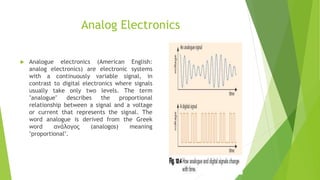
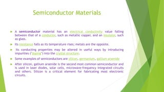
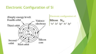
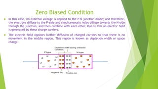
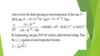
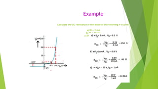
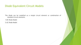
This document provides an introduction to analog electronics and discusses key concepts related to semiconductors and diodes. It defines analog electronics as systems with continuously variable signals, as opposed to digital electronics which use discrete signals. Semiconductors are described as having electrical conductivity between conductors and insulators. The document discusses n-type and p-type semiconductors, the PN junction, and diode characteristics under forward and reverse bias. Diode models including the ideal diode model and equivalent circuit models are presented. Key diode parameters such as forward and reverse resistance are also summarized.
This presentation contains the basic information you need to know about operational amplifier.
I have tried to cover all the basic info. If anything is left out or you have any suggestions i will appreciate it.
Its looks like a letter Z due to symmetrical switching characteristics for each polarity of the applied voltage. ... This means that, unlike the triac and the SCR, the disc cannot be estimated to maintain a low voltage drop until its current falls below the level of holding current. A triac is a 4-layer semiconductor device with two power terminals (MT1 and MT2) and a gate terminal. It is used as a power control device for 50/60Hz AC mains applications. It is placed in series with the load connected across the mains. ... A disc is a similar 4-layer device but does not have a gate terminal.
http://bit.ly/2PIOIQM
Introduction to operational Amplifier. For A2 level physics (CIE). Discusses characteristics of op amp, inverting and non inverting amplifier, and voltage follower, and transfer characetristics, virtual earth , etc
Original Uni-junction transistor or UJT is a simple device in which a bar of N-type semiconductor material into which P-type material is diffused; somewhere along its length defining the device parameter as intrinsic standoff. The 2N2646 is the most commonly used version of UJT.
Negative amplifiers and its types Positive feedback and Negative feedbackimtiazalijoono
Negative amplifiers
What is Feedback?
Positive feedback
Negative feedback
Feedback Circuit
Principles of Negative Voltage Feedback In Amplifiers
Gain of Negative Voltage Feedback Amplifier
Advantages of Negative Voltage Feedback
Principles of Negative Current Feedback
Current Gain with Negative Current Feedback
The three types of rectifiers in just 18 slides. Learn and enjoy the concepts. This PowerPoint presentation not only tells about the working and principles of rectifiers but also determines the disadvantages and advantages of different rectifiers. This PowerPoint presentation also has circuit diagrams that suit your necessities. This PPT can be written as an answer for a long type of question too.
dso is use for measurement ac as well as dc voltage and current.
and also use for faulty components in various circuit .it stored wave form in digital memory.it easy to operate. cursor measurement is possible.
Classification of signals and systems as well as their properties are given in the PPT .Examples related to types of signals and systems are also given .
Electrical current, voltage, resistance, capacitance, and inductance are a few of the basic elements of electronics and radio. Apart from current, voltage, resistance, capacitance, and inductance, there are many other interesting elements to electronic technology. ... Use Electronics Notes to learn electronics online.
Introduction to Semiconductor Devices.
In modern world no other technology permeates every nook and cranny of our existence as does electronics.
Application of electronics are : Televisions, radios, stereo equipment, computers, scanners, electronic control systems (in cars for example) etc.
SEMICONDUCTOR DEVICES AND APPLICATIONS.
Introduction to P-N Junction Diode and V-I Characteristics
Half wave and Full wave rectifiers
Capacitor filters
Zener diode and its Characteristics
Zener Diode as Voltage regulator
Electronics and Communication Engineering is the Branch of Engineering. Electronics and Communication Engineering field requires an understanding of core areas including Engineering Graphics, Computer Programming,Electronics Devices and Circuits-I, Network Analysis, Signals and Systems, Communication Systems, Electromagnetics Engineering, Digital Signal Processing, Embedded Systems, Microprocessor and Computer Architecture. Ekeeda offers Online Mechanical Engineering Courses for all the Subjects as per the Syllabus. Visit : https://ekeeda.com/streamdetails/stream/Electronics-and-Communication-Engineering
We have compiled the most important slides from each speaker's presentation. This year’s compilation, available for free, captures the key insights and contributions shared during the DfMAy 2024 conference.
6th International Conference on Machine Learning & Applications (CMLA 2024)ClaraZara1
6th International Conference on Machine Learning & Applications (CMLA 2024) will provide an excellent international forum for sharing knowledge and results in theory, methodology and applications of on Machine Learning & Applications.
Final project report on grocery store management system..pdfKamal Acharya
In today’s fast-changing business environment, it’s extremely important to be able to respond to client needs in the most effective and timely manner. If your customers wish to see your business online and have instant access to your products or services.
Online Grocery Store is an e-commerce website, which retails various grocery products. This project allows viewing various products available enables registered users to purchase desired products instantly using Paytm, UPI payment processor (Instant Pay) and also can place order by using Cash on Delivery (Pay Later) option. This project provides an easy access to Administrators and Managers to view orders placed using Pay Later and Instant Pay options.
In order to develop an e-commerce website, a number of Technologies must be studied and understood. These include multi-tiered architecture, server and client-side scripting techniques, implementation technologies, programming language (such as PHP, HTML, CSS, JavaScript) and MySQL relational databases. This is a project with the objective to develop a basic website where a consumer is provided with a shopping cart website and also to know about the technologies used to develop such a website.
This document will discuss each of the underlying technologies to create and implement an e- commerce website.
Sachpazis:Terzaghi Bearing Capacity Estimation in simple terms with Calculati...Dr.Costas Sachpazis
Terzaghi's soil bearing capacity theory, developed by Karl Terzaghi, is a fundamental principle in geotechnical engineering used to determine the bearing capacity of shallow foundations. This theory provides a method to calculate the ultimate bearing capacity of soil, which is the maximum load per unit area that the soil can support without undergoing shear failure. The Calculation HTML Code included.
Using recycled concrete aggregates (RCA) for pavements is crucial to achieving sustainability. Implementing RCA for new pavement can minimize carbon footprint, conserve natural resources, reduce harmful emissions, and lower life cycle costs. Compared to natural aggregate (NA), RCA pavement has fewer comprehensive studies and sustainability assessments.
Forklift Classes Overview by Intella PartsIntella Parts
Discover the different forklift classes and their specific applications. Learn how to choose the right forklift for your needs to ensure safety, efficiency, and compliance in your operations.
For more technical information, visit our website https://intellaparts.com
Overview of the fundamental roles in Hydropower generation and the components involved in wider Electrical Engineering.
This paper presents the design and construction of hydroelectric dams from the hydrologist’s survey of the valley before construction, all aspects and involved disciplines, fluid dynamics, structural engineering, generation and mains frequency regulation to the very transmission of power through the network in the United Kingdom.
Author: Robbie Edward Sayers
Collaborators and co editors: Charlie Sims and Connor Healey.
(C) 2024 Robbie E. Sayers
2. Electronics
The branch of physics that deals with the emission and effects of electrons
and with the use of electronic devices.
The use and study of electricity in semiconductors.
The branch of engineering in which the flow and control of electrons in
vacuum or semiconductor are studied is called electronics.
3. Analog Electronics
Analogue electronics (American English:
analog electronics) are electronic systems
with a continuously variable signal, in
contrast to digital electronics where signals
usually take only two levels. The term
"analogue" describes the proportional
relationship between a signal and a voltage
or current that represents the signal. The
word analogue is derived from the Greek
word ανάλογος (analogos) meaning
"proportional".
4. Electronic Devices and Circuits
The device which controls the flow of electrons is called electronic device.
These devices are the main building blocks of electronic circuits.
Electronics have various branches include, digital electronics, analog
electronics, micro electronics, nanoelectronics, optoelectronics, integrated
circuit and semiconductor device.
An electronic circuit is composed of individual electronic components, such as
resistors, transistors, capacitors, inductors and diodes, connected by
conductive wires or traces through which electric current can flow. To be
referred to as electronic, rather than electrical, generally at least one active
component must be present. The combination of components and wires
allows various simple and complex operations to be performed: signals can be
amplified, computations can be performed, and data can be moved from one
place to another.
9. Semiconductor Materials
A semiconductor material has an electrical conductivity value falling
between that of a conductor, such as metallic copper, and an insulator, such
as glass.
Its resistance falls as its temperature rises; metals are the opposite.
Its conducting properties may be altered in useful ways by introducing
impurities ("doping") into the crystal structure.
Some examples of semiconductors are silicon, germanium, gallium arsenide
After silicon, gallium arsenide is the second most common semiconductor and
is used in laser diodes, solar cells, microwave-frequency integrated circuits
and others. Silicon is a critical element for fabricating most electronic
circuits.
10. Semiconductor materials
Silicon (Si) and germanium (Ge) are well-known semiconductor materials.
When they are pure crystals, these substances are close to insulators (intrinsic
semiconductors), but doping a small amount of dopant causes the
electrical resistance to drop greatly, turning them into conductors.
Depending on the kind of dopant, n-type or p-type semiconductor can be
made.
Semiconductors made of several elements are called compound
semiconductors, as opposed to those made of a single element such as silicon
semiconductors. There are combinations such as Group III and Group V of the
periodic table, Group II and Group VI, Group IV, etc.
16. What is a n-type Semiconductor?
An n-type semiconductor is an intrinsic semiconductor doped with phosphorus
(P), arsenic (As), or antimony (Sb) as an impurity. Silicon of Group IV has four
valence electrons and phosphorus of Group V has five valence electrons. If a
small amount of phosphorus is added to a pure silicon crystal, one of the
valence electrons of phosphorus becomes free to move around (free
electron*) as a surplus electron. When this free electron is attracted to the
“+” electrode and moves, current flows.
18. What is a p-type Semiconductor?
A p-type semiconductor is an intrinsic semiconductor doped with boron (B) or
indium (In). Silicon of Group IV has four valence electrons and boron of Group
III has three valence electrons. If a small amount of boron is doped to a single
crystal of silicon, valence electrons will be insufficient at one position to bond
silicon and boron, resulting in holes* that lack electrons. When a voltage is
applied in this state, the neighboring electrons move to the hole, so that the
place where an electron is present becomes a new hole, and the holes appear
to move to the "–" electrode in sequence.
21. PN Junction
The contact surface between a p-type and an n-type semiconductor is called
a PN junction. When p-type and n-type semiconductors are bonded, holes and
free electrons, which are carriers, are attracted and bound and disappear
near the boundary. Since there are no carriers in this area, it is called a
depletion layer and it is in the same state as an insulator.
In this state, connecting the “+” pole to the p-type region, connecting the “-”
pole to the n-type region and applying a voltage cause electrons to flow
sequentially from the n-type to the p-type region. The electrons will first
disappear by combining with holes, but excess electrons move to the “+” pole
and current will flow.
24. A semiconductor Diode
A semiconductor diode is a device typically made up of a single p-n junction.
The junction of a p-type and n-type semiconductor forms a depletion region
where current conduction is reserved by the lack of mobile charge carriers.
When the device is forward biased, this depletion region is reduced, allowing
for significant conduction, when the diode is reverse biased, the only less
current can be achieved and the depletion region can be extended.
Exposing a semiconductor to light can produce electron hole pairs, which
increases the number of free carriers and thereby the conductivity. Diodes
optimized to take advantage of this phenomenon is known as photodiodes.
Compound semiconductor diodes are also being used to generate light, light-
emitting diodes and laser diodes.
26. PN Junction Diode Theory
Based on the applied voltage, there are three possible “biasing” conditions for
the P-N Junction Diode, which are as follows:
Zero Bias – No external voltage is applied to the PN junction diode.
Forward Bias– The voltage potential is connected positively to the P-type
terminal and negatively to the N-type terminal of the Diode.
Reverse Bias– The voltage potential is connected negatively to the P-type
terminal and positively to the N-type terminal of the Diode.
27. Zero Biased Condition
In this case, no external voltage is applied to the P-N junction diode; and therefore,
the electrons diffuse to the P-side and simultaneously holes diffuse towards the N-side
through the junction, and then combine with each other. Due to this an electric field
is generated by these charge carriers.
The electric field opposes further diffusion of charged carriers so that there is no
movement in the middle region. This region is known as depletion width or space
charge.
29. Forward Bias
In the forward bias condition, the negative terminal of the battery is
connected to the N-type material and the positive terminal of the battery is
connected to the P-Type material.
Electrons from the N-region cross the junction and enters the P-region. Due to
the attractive force that is generated in the P-region the electrons are
attracted and move towards the positive terminal.
Simultaneously the holes are attracted to the negative terminal of the
battery. By the movement of electrons and holes current flows.
In this forward bias condition, the width of the depletion region decreases
due to the reduction in the number of positive and negative ions.
31. V-I Characteristics
By supplying positive voltage, the electrons get enough energy to overcome the potential
barrier (depletion layer) and cross the junction and the same thing happens with the holes
as well. The amount of energy required by the electrons and holes for crossing the junction
is equal to the barrier potential 0.3 V for Ge and 0.7 V for Si, 1.2V for GaAs. This is also
known as Voltage drop.
33. Reverse Bias
When a diode is connected in a Reverse Bias condition, a positive voltage is
applied to the N-type material and a negative voltage is applied to the P-type
material.
The positive voltage applied to the N-type material attracts electrons towards
the positive electrode and away from the junction, while the holes in the P-
type end are also attracted away from the junction towards the negative
electrode.
The net result is that the depletion layer grows wider due to a lack of
electrons and holes and presents a high impedance path, almost an insulator.
The result is that a high potential barrier is created thus preventing current
from flowing through the semiconductor material.
40. Semiconductor Devices
Electronic parts using semiconductors are called semiconductor devices.
Many kinds of semiconductor devices have been developed in line with the
expansion of application fields and the progress of electronic equipment.
“Discrete semiconductors” are single devices with a single function, such as
transistors and diodes.
“Integrated circuits (ICs)” are devices with multiple functional elements
mounted on one chip. Typical ICs include memories, microprocessors (MPUs),
and logic Ics.
42. Diode current equation
Diode current equation expresses the relationship between the current
flowing through the diode as a function of the voltage applied across it.
Mathematically it is given as
Where,
I is the current flowing through the diode
I0 is the dark saturation current,
q is the charge on the electron,
V is the voltage applied across the diode,
η is the (exponential) ideality factor.
is the Boltzmann constant
T is the absolute temperature in Kelvin.
43. That is, if the diode under consideration behaves exactly as that of an ideal
diode, then η will be 1
The value of η is typically considered to be 1 for germanium diodes and 2 for
silicon diodes.
However, its exact value for the given diode depends on various factors like
electron drift, diffusion, carrier recombination which occurs within the
depletion region, its doping level, manufacturing technique and the purity of
its materials.
44. In forward biased condition, there will a large amount of current flow
through the diode. Thus the diode current equation (equation 1) becomes
On the other hand, if the diode is reverse biased, then the exponential term
in equation (1) becomes negligible. Thus we have
45. when we have the diode operating at roomtemperature. In this case, T =
300 K, also, and . Thus
By reciprocating, one gets, 25.87 mV which is called thermal voltage. Thus
the diode equation at room temperature becomes
49. Diode Resistance - Static,Dynamic and
Reverse Resistance
The diode does not allow the current completely under forward bias and does not
block the current in the reverse bias.
Ideally, the diode must have zero resistance in forward biasing and infinite
resistance in reverse biasing.
When forward biased is applied the width of the depletion layer gets
decreased. However, the depletion layer can't be completely eradicated. The
thin layer of depletion layer is always exist.
The resistance offered by this thin layer of depletion region under forward
biased state is called forward resistance of the diode.
Under reverse biasing, the diode offers very large resistance to the electric
current. This resistance is called the reverse resistance.
50. There are two types of resistance of p-n junction diode.
1. Forward Resistance
2. Reverse Resistance
The resistance of the forward biased diode is called forward resistance. The forward resistance can be
further grouped into two category.
1. Static Resistance or DC resistance
2. Dynamic Resistance or AC resistance
51. Example
Calculate the DC resistance of the diode of the following V-I curve.
a) ID = 2 mA
b) ID = 20 mA
c) VD = -10 Volts
52. Static Resistance or DC Forward Resistance
When DC is fed to diode, the current flows in one direction. The resistance
offered by the diode is called the DC resistance.
53. Dynamic Resistance or AC Forward Resistance
The resistance offered by the diode when AC is applied to the diode is called AC resistance or
dynamic resistance. The current flows in both the direction when AC voltage is applied.
The ratio of change in voltage to change in current represent
dynamic resistance of the diode. It is denoted by rac .
54. Reverse Resistance
When reverse bias is applied to p-n junction diode, the width of the depletion
layer increase and it offers higher resistance to the flow of charge carriers.
The reverse resistance of p-n diode is in order of mega ohms. The reverse
resistance is very large compared to the forward resistance of the diode.
57. Diode Equivalent Circuit Models
The diode can be modelled as a simple circuit element or combination of
standard circuit elements.
1.DC Diode Model
2.AC Diode Model
58. DC Diode Model
Ideal diode: VON= 0, Rr = ∞ and Rf = 0. In other words, the ideal diode is a
short in the forward bias region and an open in the reverse bias region.
Practical diode (silicon): VON = 0.7V, Rr < ∞ (typically several MΩ), Rf ≈rd
(typically < 50 Ω).
59. general representation for a practical
diode under dc operating conditions
For the forward bias region (vD≥ 0.7 V for silicon),
the ideal diode is a short and the terminal
characteristics of the model abovereduce to the
parallel combination of Rr and Rf. Since Rr >> Rf,
Rr ||Rf≈ Rf.
60. Dc models of diode in forward and
reverse bias
Likewise, when the voltage applied to the diode is less than VON (vD < 0.7
V)for silicon), the ideal diode is an open and the resistance between
terminals a and b is Rr.
diode characteristics in the forward and reverse bias regions are quite distinct
61. AC Diode Model under reverse bias
The charge separation comes in the diode due to the depletion region, which
in turn dependent on the applied bias.
For the reverse bias case, this introduces a junction capacitance (Cj) in
parallel with the reverse bias resistance (Rr)
62. AC Diode Model under forward bias
Since current flow is moving charge, we’ve got charges moving in
the semiconductor material. Charges cannot move
instantaneously, so there is a “charge storage” effect that leads
to a diffusion capacitance (CD). The forward bias resistance is also
a function of frequency, so the dynamic resistance, rd, replaces
the constant Rf term.
63. Load line
In graphical analysis of nonlinear electronic circuits, a load line is a line
drawn on the characteristic curve, a graph of the current vs. the voltage in a
nonlinear device like a diode or transistor. It represents the constraint put on
the voltage and current in the nonlinear device by the external circuit
The load line, usually a straight line, represents the response of the linear
part of the circuit, connected to the nonlinear device in question
64. What is a DC Load Line?
A circuit supplied with dc power as the external source of the circuit. There
exist both alternating and direct currents in the circuit. The reactive
components of the circuits are made zero and the straight line is drawn above
the voltage-current characteristics curves. Hence these results in the
formation of intersecting point referred to an operating point. The straight
line that is drawn for this purpose is defined as the DC load line.
66. The characteristic curve (curved line), representing the current I
through the diode for any given voltage across the diode VD, is an
exponential curve. The load line (diagonal line) represents the
relationship between current and voltage due to Kirchhoff's voltage
law applied to the resistor and voltage source, is
Since the current going through the three elements in series must be
the same, and the voltage at the terminals of the diode must be the
same, the operating point of the circuit will be at the intersection of
the curve with the load line.