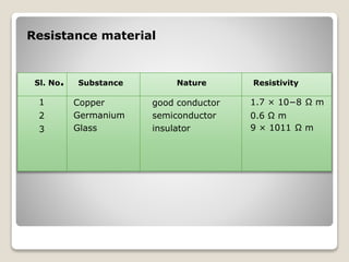
This document discusses semiconductors and provides details about their properties and characteristics. It defines a semiconductor as a material with resistivity between that of a conductor and insulator. Some key points made in the document are:
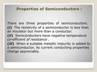
- Semiconductors have properties like negative temperature coefficient of resistance and their conductivity can change when doped with impurities.
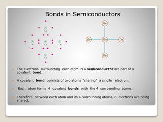
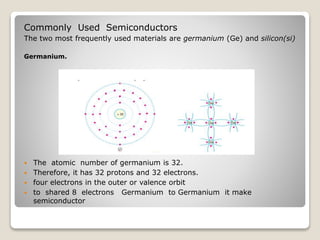
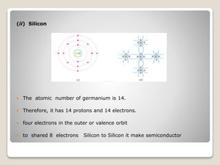
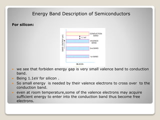
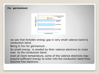
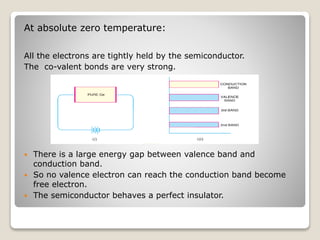
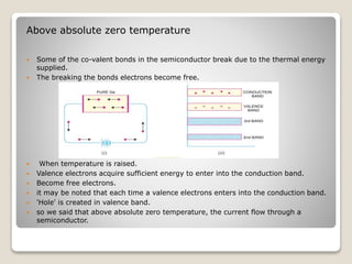
- Common semiconductors include silicon and germanium which form covalent bonds and have small energy gaps between valence and conduction bands.
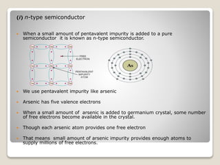
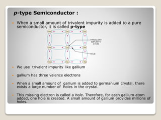
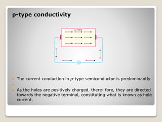
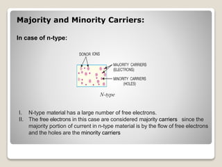
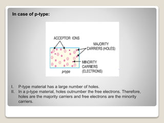
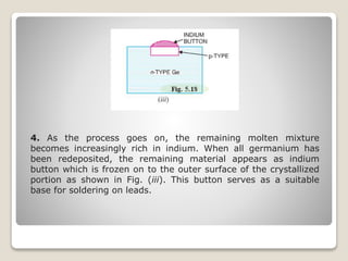
- Semiconductors can be doped as n-type or p-type to introduce free electrons or holes that serve as majority carriers for current flow. A pn junction is formed when a p-type and n-


![[Deck] What's New in Spark-Iceberg Integration via DSV2.pptx](https://cdn.slidesharecdn.com/ss_thumbnails/deckwhatsnewinspark-icebergintegrationviadsv2-260210005337-25955b12-thumbnail.jpg?width=640&height=640&fit=bounds)


