Download to read offline
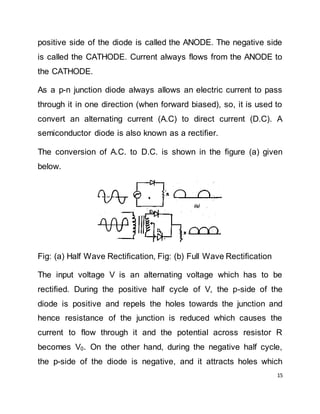
![22
opposite to the emitter) that collects the charge carriers (i.e.
electrons or holes) [is called the collector]. The collector is always
larger than the emitter and the base of a transistor. The doping
level of the collector is in between the heavy doping of the emitter
and the light doping of the base. In both PNP and NPN transistors
the collector base junction always should be reverse biased.
Collector of PNP transistor receives hole charges that flow in the
output circuit. Similarly, the collector of NPN transistor receives
electrons.
Emitter of a Transistor
The portion on one side of transistor that supplies charge carriers
(i.e. electrons or holes) to the other two portions (is called
emitter). The emitter is a heavily doped region. The emitter is
always forward biased with respect to base so that it can supply a
large number of majority carriers. In both PNP and NPN
transistors emitter base junction always should be forward biased.
Emitter of PNP transistor supplies hole charges to its junction with
the base. Similarly, the emitter of NPN transistor supplies free
electrons to its junction with the base.](https://image.slidesharecdn.com/moduleno-200324163633/85/Module-No-25-22-320.jpg)

Majority and minority charge carriers are defined for p-type and n-type semiconductors. In p-type semiconductors, holes are the majority carriers while electrons are the minority carriers. In n-type semiconductors, electrons are the majority carriers and holes are the minority carriers. Semiconductors are doped with impurities to increase the number of majority carriers, making the material either p-type or n-type. A depletion region forms at the PN junction where majority carriers diffuse across and recombine, leaving an area devoid of carriers.