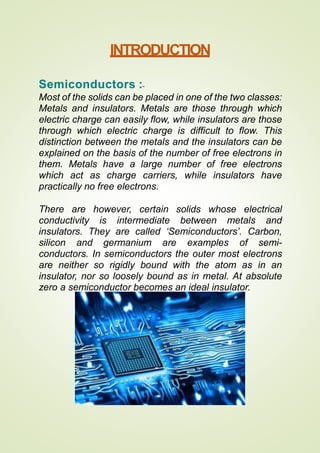
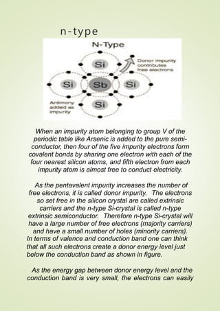
GUIDED BY :- SUBMISSIONTED BY
SHIVAM JHADE
CLASS-XIIA SEC-A
ROLL NO- 24
BOARD ROLL NO-
YEAR-2020-21
PHYSICS INVESTIGATORY PROJECT
ON
SEMICONDUCTORS
NRI GLOBAL DISCOVERY SCHOOL BHOPAL
TEACHERPRINCIPAL
ACKNOLEGMENT
I would like to express my special
thanks of gratitude to my teacher
(Name of the teacher) as well as
our principal (Name of the
principal)who gave me the golden
opportunity to do this wonderful
project on the topic
(SEMICONDUCTOR), which also
helped me in doing a lot of
Research and i came to know
about so many new things I am
really thankful to them.
Secondly i would also like to thank
my parents and friends who
helped me a lot in finalizing this
project within the limited time
frame.
DATE:-
SHIVAM JHADE
XII A
INDEX
1. INTRODUCTION
2.Theory a n d Definition
3 . E f f e c t o f t e m p e r a t u r e on
conductivity o f Semiconductor
4. INTRINSIC SEMICONDUCTORS
5 . e x t r i n s i c semiconductors
· n-type semiconductor
7. p-type semiconductor
8 . e l e c t r i c a l r e s i s t i v i t y o f
semiconductors
INTRODUCTION
Semiconductors :-
Most of the solids can be placed in one of the two classes:
Metals and insulators. Metals are those through which
electric charge can easily flow, while insulators are those
through which electric charge is difficult to flow. This
distinction between the metals and the insulators can be
explained on the basis of the number of free electrons in
them. Metals have a large number of free electrons
which act as charge carriers, while insulators have
practically no free electrons.
There are however, certain solids whose electrical
conductivity is intermediate between metals and
insulators. They are called ‘Semiconductors’. Carbon,
silicon and germanium are examples of semi-
conductors. In semiconductors the outer most electrons
are neither so rigidly bound with the atom as in an
insulator, nor so loosely bound as in metal. At absolute
zero a semiconductor becomes an ideal insulator.
Theory and
Definition
 Semiconductors are the materials whose
electrical conductivity lies in between metals
and insulator.
The energy band structure of the semiconductors
is similar to the insulators but in their case, the size of
the
 forbidden energy gap is much smaller than that of the
insulator. In this class of crystals, the forbidden gap is of
 the order of about 1ev, and the two energy bands are
distinctly separate with no overlapping. At absolute
o0,
 no electron has any energy even to jump the forbidden gap
and reach the conduction band. Therefore
the
 substance is an insulator.
But when we heat the crystal and thus provide some energy to
the atoms and their electrons, it becomes an easy matter for
some electrons to jump the small (» 1 ev) energy gap and go to
conduction band. Thus at higher temperatures, the crystal
becomes a conductors. This is the specific property of the crystal
which is known as a semiconductor.
E f f e c t o f t e m p e r a t u r e on
conductivity o f Semiconductor
At 0K, all semiconductors are insulators. The valence
band at absolute zero is completely filled and there are
no free electrons in conduction band. At room
temperature the electrons jump to the conduction band
due to the thermal energy. When the temperature
increases, a large number of electrons cross over the
forbidden gap and jump from valence to conduction band.
Hence conductivity of semiconductor increases with
temperature.
INTRINSIC SEMICONDUCTORS
Pure semiconductors are called intrinsic semi-conductors. In
a pure semiconductor, each atom behaves as if thereare
8 electrons in its valence shell and therefore the entire
material behaves as an insulator at low temperatures.
A semiconductor atom needs energy of the order of 1.1ev
to shake off the valence electron. This energy becomes
available to it even at room temperature.
Due to thermal agitation of crystal structure, electrons
from a few covalent bonds come out. The bond from
which electron is freed, a vacancy is created there. The
vacancy in the covalent bond is called a hole.
This hole can be filled by some other electron in a
covalent bond. As an electron from covalent bond moves
to fill the hole, the hole is created in the covalent bond
from which the electron has moved. Since the direction
of movement of the hole is opposite to that of the negative
electron, a hole behaves as a positive
carrier. Thus, at room temperature,
charge
a pure
semiconductor will have electrons and holes wandering
in random directions. These electrons and holes are
called intrinsic carriers.
As the crystal is neutral, the number of free electrons will
be equal to the number of holes. In an intrinsic
semiconductor, if ne denotes the electron number density
in conduction band, nh the hole number density in
valence band and ni the number density or concentration
of charge carriers, then
ne = nh =ni
extrinsic semiconductors
 As the conductivity of intrinsic semi-conductors is poor, so
intrinsic semi-conductors are of little practical importance. The
conductivity of pure semi-conductor can, however be
enormously increased by addition of some pentavalent or a
trivalent impurity in a very small amount (about 1 to 106 parts of
the semi-conductor). The process of adding an impurity to a
pure semiconductor so as to improve its conductivity is called
doping. Such semi-conductors are called extrinsic semi-
conductors. Extrinsic semiconductors are of two types :
i)
ii)
n-type semiconductor
p-type semiconductor
n-type
semiconductor
When an impurity atom belonging to group V of the
periodic table like Arsenic is added to the pure semi-
conductor, then four of the five impurity electrons form
covalent bonds by sharing one electron with each of the
four nearest silicon atoms, and fifth electron from each
impurity atom is almost free to conduct electricity.
As the pentavalent impurity increases the number of
free electrons, it is called donor impurity. The electrons
so set free in the silicon crystal are called extrinsic
carriers and the n-type Si-crystal is called n-type
extrinsic semiconductor. Therefore n-type Si-crystal will
have a large number of free electrons (majority carriers)
and have a small number of holes (minority carriers).
In terms of valence and conduction band one can think
that all such electrons create a donor energy level just
below the conduction band as shown in figure.
As the energy gap between donor energy level and the
conduction band is very small, the electrons can easily
raise themselves to conduction band even at room
temperature. Hence, the conductivity of n-type extrinsic
semiconductor is markedly increased.
In a doped or extrinsic semiconductor, the number
density of the conduction band (ne) and the number
density of holes in the valence band (nh) differ from that
in a pure semiconductor. If ni is the number density of
electrons is conduction band, then it is proved that
ne nh =ni2
p-type semiconductor
If a trivalent impurity like indium is added in pure semi-
conductor, the impurity atom can provide only three
valence electrons for covalent bond formation. Thus a
gap is left in one of the covalent bonds. The gap acts as
a hole that tends to accept electrons. As the trivalent
impurity atoms accept electrons from the silicon crystal,it
is called acceptor impurity. The holes so created are
extrinsic carriers and the p-type Si-crystal so obtained is
called p-type extrinsic semiconductor. Again, as the pure
Si-crystal also possesses a few electrons and holes,
therefore, the p-type si-crystal will have a large number
of holes (majority carriers) and a small number of
electrons (minority carriers).
It terms of valence and conduction band one can think
that all such holes create an accepter energy level just
above the top of the valance band as shown in figure.
The electrons from valence band can raise themselves
to the accepter energy level by absorbing thermal
energy at room temperature and in turn create holes in
the valence band.
Number density of valence band holes (nh) in p-type
semiconductor is approximately equal to that of the
acceptor atoms (Na) and is very large as compared to the
number density of conduction band electrons (ne). Thus,
nh» Na > > ne
e l e c t r i c a l r e s i s t i v i t y o f
semiconductors
Consider a block of semiconductor of length l1 area of
cross-section A and having number density of electrons
and holes as ne and nh respectively. Suppose that on
applying a potential difference, say V, a current I flows
through it as shown in figure. The electron current (Ic)
and the hole current (Ih) constitute the current I flowing
through the semi conductor i.e.
I=Ie +Ih (i)
It ne is the number density of conduction
band electrons in the semiconductor and ve, the drift
velocity of electrons then
Ie = eneAve
Similarly, the hole current, Ih = enhAvh
From (i) I = eneAve + enhAvh
I=eA(neve +nhvh) (ii)
If r is the resistivity of the material of the
semiconductor, then the resistance offered by the
semiconductor to the flow of current is given by :
R=  l/A (iii)
Since V = RI, from equation (ii) and (iii) we have
V = RI =  l/A eA (neve + nh vh)
V=  le(neve +nhvh) (iv)
If E is the electric field set up across the semiconductor,
then:
E=V/l (v)
from equation (iv) and (v), we have
E = e (neve + nhvh)
1/ = e (ne ve/E + nh vh/E)
On applying electric field, the drift velocity
acquired by the electrons (or holes) per unit strength of
electric field is called mobility of electrons (or holes).
Therefore,
mobility of electrons and holes is given by :
e = ve/E and h = vh/E
1/ =e(ne e +nh h) (vi)
Also,  = 1/ is called conductivity of the material
of semiconductor
 =e(ne e +nh h) (vii)
The relation (vi) and (vii) show that the conductivity and
resistivity of a semiconductor depend upon the electron
and hole number densities and their mobilities. As
ne and nh increases with rise in temperature, therefore,
conductivity of semiconductor increases with rise in
temperature and resistivity decreases with rise in
temperature.
.
.
bibl o g r a p h y
1.www.google.com
2.www.wikipedia.com
3.www.ncert.nic.in
4.Pradeep class 12 Physics
5.HC verma class 12 Physics
TheEnd

INVESTIGATORY PROJECT ON SEMICONDUCTOR by shivam jhade

  • 1.
    GUIDED BY :-SUBMISSIONTED BY SHIVAM JHADE CLASS-XIIA SEC-A ROLL NO- 24 BOARD ROLL NO- YEAR-2020-21 PHYSICS INVESTIGATORY PROJECT ON SEMICONDUCTORS NRI GLOBAL DISCOVERY SCHOOL BHOPAL TEACHERPRINCIPAL
  • 2.
    ACKNOLEGMENT I would liketo express my special thanks of gratitude to my teacher (Name of the teacher) as well as our principal (Name of the principal)who gave me the golden opportunity to do this wonderful project on the topic (SEMICONDUCTOR), which also helped me in doing a lot of Research and i came to know about so many new things I am really thankful to them. Secondly i would also like to thank my parents and friends who helped me a lot in finalizing this project within the limited time frame. DATE:- SHIVAM JHADE XII A
  • 3.
    INDEX 1. INTRODUCTION 2.Theory an d Definition 3 . E f f e c t o f t e m p e r a t u r e on conductivity o f Semiconductor 4. INTRINSIC SEMICONDUCTORS 5 . e x t r i n s i c semiconductors · n-type semiconductor 7. p-type semiconductor 8 . e l e c t r i c a l r e s i s t i v i t y o f semiconductors
  • 4.
    INTRODUCTION Semiconductors :- Most ofthe solids can be placed in one of the two classes: Metals and insulators. Metals are those through which electric charge can easily flow, while insulators are those through which electric charge is difficult to flow. This distinction between the metals and the insulators can be explained on the basis of the number of free electrons in them. Metals have a large number of free electrons which act as charge carriers, while insulators have practically no free electrons. There are however, certain solids whose electrical conductivity is intermediate between metals and insulators. They are called ‘Semiconductors’. Carbon, silicon and germanium are examples of semi- conductors. In semiconductors the outer most electrons are neither so rigidly bound with the atom as in an insulator, nor so loosely bound as in metal. At absolute zero a semiconductor becomes an ideal insulator.
  • 5.
    Theory and Definition  Semiconductorsare the materials whose electrical conductivity lies in between metals and insulator. The energy band structure of the semiconductors is similar to the insulators but in their case, the size of the  forbidden energy gap is much smaller than that of the insulator. In this class of crystals, the forbidden gap is of  the order of about 1ev, and the two energy bands are distinctly separate with no overlapping. At absolute o0,  no electron has any energy even to jump the forbidden gap and reach the conduction band. Therefore the  substance is an insulator. But when we heat the crystal and thus provide some energy to the atoms and their electrons, it becomes an easy matter for some electrons to jump the small (» 1 ev) energy gap and go to conduction band. Thus at higher temperatures, the crystal becomes a conductors. This is the specific property of the crystal which is known as a semiconductor.
  • 6.
    E f fe c t o f t e m p e r a t u r e on conductivity o f Semiconductor At 0K, all semiconductors are insulators. The valence band at absolute zero is completely filled and there are no free electrons in conduction band. At room temperature the electrons jump to the conduction band due to the thermal energy. When the temperature increases, a large number of electrons cross over the forbidden gap and jump from valence to conduction band. Hence conductivity of semiconductor increases with temperature. INTRINSIC SEMICONDUCTORS Pure semiconductors are called intrinsic semi-conductors. In a pure semiconductor, each atom behaves as if thereare
  • 7.
    8 electrons inits valence shell and therefore the entire material behaves as an insulator at low temperatures. A semiconductor atom needs energy of the order of 1.1ev to shake off the valence electron. This energy becomes available to it even at room temperature. Due to thermal agitation of crystal structure, electrons from a few covalent bonds come out. The bond from which electron is freed, a vacancy is created there. The vacancy in the covalent bond is called a hole. This hole can be filled by some other electron in a covalent bond. As an electron from covalent bond moves to fill the hole, the hole is created in the covalent bond from which the electron has moved. Since the direction of movement of the hole is opposite to that of the negative electron, a hole behaves as a positive carrier. Thus, at room temperature, charge a pure semiconductor will have electrons and holes wandering in random directions. These electrons and holes are called intrinsic carriers. As the crystal is neutral, the number of free electrons will be equal to the number of holes. In an intrinsic semiconductor, if ne denotes the electron number density in conduction band, nh the hole number density in valence band and ni the number density or concentration of charge carriers, then ne = nh =ni
  • 8.
    extrinsic semiconductors  Asthe conductivity of intrinsic semi-conductors is poor, so intrinsic semi-conductors are of little practical importance. The conductivity of pure semi-conductor can, however be enormously increased by addition of some pentavalent or a trivalent impurity in a very small amount (about 1 to 106 parts of the semi-conductor). The process of adding an impurity to a pure semiconductor so as to improve its conductivity is called doping. Such semi-conductors are called extrinsic semi- conductors. Extrinsic semiconductors are of two types : i) ii) n-type semiconductor p-type semiconductor
  • 9.
    n-type semiconductor When an impurityatom belonging to group V of the periodic table like Arsenic is added to the pure semi- conductor, then four of the five impurity electrons form covalent bonds by sharing one electron with each of the four nearest silicon atoms, and fifth electron from each impurity atom is almost free to conduct electricity. As the pentavalent impurity increases the number of free electrons, it is called donor impurity. The electrons so set free in the silicon crystal are called extrinsic carriers and the n-type Si-crystal is called n-type extrinsic semiconductor. Therefore n-type Si-crystal will have a large number of free electrons (majority carriers) and have a small number of holes (minority carriers). In terms of valence and conduction band one can think that all such electrons create a donor energy level just below the conduction band as shown in figure. As the energy gap between donor energy level and the conduction band is very small, the electrons can easily
  • 10.
    raise themselves toconduction band even at room temperature. Hence, the conductivity of n-type extrinsic semiconductor is markedly increased. In a doped or extrinsic semiconductor, the number density of the conduction band (ne) and the number density of holes in the valence band (nh) differ from that in a pure semiconductor. If ni is the number density of electrons is conduction band, then it is proved that ne nh =ni2 p-type semiconductor If a trivalent impurity like indium is added in pure semi- conductor, the impurity atom can provide only three valence electrons for covalent bond formation. Thus a gap is left in one of the covalent bonds. The gap acts as a hole that tends to accept electrons. As the trivalent impurity atoms accept electrons from the silicon crystal,it
  • 11.
    is called acceptorimpurity. The holes so created are extrinsic carriers and the p-type Si-crystal so obtained is called p-type extrinsic semiconductor. Again, as the pure Si-crystal also possesses a few electrons and holes, therefore, the p-type si-crystal will have a large number of holes (majority carriers) and a small number of electrons (minority carriers). It terms of valence and conduction band one can think that all such holes create an accepter energy level just above the top of the valance band as shown in figure. The electrons from valence band can raise themselves to the accepter energy level by absorbing thermal energy at room temperature and in turn create holes in the valence band. Number density of valence band holes (nh) in p-type semiconductor is approximately equal to that of the acceptor atoms (Na) and is very large as compared to the number density of conduction band electrons (ne). Thus, nh» Na > > ne e l e c t r i c a l r e s i s t i v i t y o f semiconductors Consider a block of semiconductor of length l1 area of cross-section A and having number density of electrons and holes as ne and nh respectively. Suppose that on applying a potential difference, say V, a current I flows through it as shown in figure. The electron current (Ic) and the hole current (Ih) constitute the current I flowing through the semi conductor i.e. I=Ie +Ih (i)
  • 12.
    It ne isthe number density of conduction band electrons in the semiconductor and ve, the drift velocity of electrons then Ie = eneAve Similarly, the hole current, Ih = enhAvh From (i) I = eneAve + enhAvh I=eA(neve +nhvh) (ii) If r is the resistivity of the material of the semiconductor, then the resistance offered by the semiconductor to the flow of current is given by : R=  l/A (iii) Since V = RI, from equation (ii) and (iii) we have V = RI =  l/A eA (neve + nh vh) V=  le(neve +nhvh) (iv) If E is the electric field set up across the semiconductor, then: E=V/l (v) from equation (iv) and (v), we have E = e (neve + nhvh) 1/ = e (ne ve/E + nh vh/E) On applying electric field, the drift velocity acquired by the electrons (or holes) per unit strength of electric field is called mobility of electrons (or holes). Therefore, mobility of electrons and holes is given by : e = ve/E and h = vh/E 1/ =e(ne e +nh h) (vi) Also,  = 1/ is called conductivity of the material of semiconductor  =e(ne e +nh h) (vii) The relation (vi) and (vii) show that the conductivity and resistivity of a semiconductor depend upon the electron
  • 13.
    and hole numberdensities and their mobilities. As ne and nh increases with rise in temperature, therefore, conductivity of semiconductor increases with rise in temperature and resistivity decreases with rise in temperature. . .
  • 14.
    bibl o gr a p h y 1.www.google.com 2.www.wikipedia.com 3.www.ncert.nic.in 4.Pradeep class 12 Physics 5.HC verma class 12 Physics
  • 15.