Download to read offline

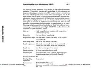
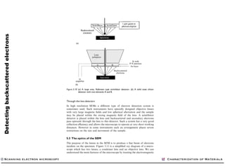

The document discusses scanning electron microscopy (SEM) and its use in characterizing materials. SEM uses an electron beam focused into a probe that scans over a sample, creating signals like secondary electrons and backscattered electrons. These signals are detected and used to form a magnified image of the sample's surface on a cathode ray tube. SEM provides higher magnification than light microscopes, with a greater depth of field. It is capable of elemental analysis and mapping at magnifications from around 10x to 300,000x, with typical operating ranges of 500eV-50keV beam energy.


