Introduction: Why SEMis Needed
• Optical microscopes are limited by the wavelength of
visible light (≈ 400–700 nm), restricting resolution to
about 200 nm.
• SEM overcomes this limitation by using electrons with
much shorter wavelengths (≈ 0.005 nm), enabling
nanometer-scale imaging.
• Provides high-resolution (≈ 1nm) surface topography,
morphology, and compositional details of materials.
• Widely used in materials science, nanotechnology,
biology, and failure analysis.
3.
Principle of SEM
•SEM works by scanning a focused beam of high-
energy electrons across a specimen surface.
• These electrons interact with atoms in the sample,
producing various signals (secondary, backscattered,
X-rays).
• Detectors collect these emitted signals to form an
image or perform analysis.
• The image brightness corresponds to signal intensity,
revealing topographical and compositional contrasts.
4.
Instrumentation of SEM
Thesecan be broadly divided
into three parts:
• Electron Column,
• Sample Column
• and Detection & Imaging
System.
5.
1. Electron Column
Theelectron column is the heart of the SEM, it produces,
accelerates, focuses, and directs the electron beam onto the
specimen.
• a) Electron Gun (Source)
• Purpose: To generate a stable beam of high-energy electrons.
• Types:
– Thermionic Emission Guns – Use heat to release electrons.
• Tungsten Filament: Inexpensive, robust, but limited
brightness.
• LaB₆ (Lanthanum Hexaboride): Brighter and longer-
lasting than tungsten.
– Field Emission Guns (FEG):
• Emit electrons under strong electric field.
• Provide high brightness and small energy spread.
• Excellent for high-resolution imaging (sub-nanometer).
6.
• b) Anode
•Accelerates electrons toward the specimen.
• Acceleration voltage: typically 0.5–30 kV depending on sample
and analysis type.
• c) Condenser Lens System
• Controls the beam diameter and current.
• Adjusts the spot size — smaller spots give higher resolution,
larger spots provide higher signal.
• d) Scanning Coils
• Deflect the focused beam across the specimen in a raster
pattern.
• Controlled electronically to synchronize with image formation.
• e) Objective Lens
• Final focusing element before the beam hits the sample.
• Defines working distance (distance from lens to sample).
• May include stigmators to correct astigmatism in the beam.
7.
2. Sample Column
Thearea where the sample is mounted and examined.
• a) Sample Stage
• Allows X, Y, Z, tilt, and rotation adjustments.
• Enables imaging from different angles and magnifications.
• b) Vacuum System
• Prevents electron scattering by air molecules.
• Comprises:
– Roughing Pump: Lowers pressure to ~10⁻² mbar.
– High-Vacuum Pump (Turbomolecular or Ion Pump): Achieves
pressures up to 10⁻⁵–10⁻⁷ mbar.
• Some SEMs operate in Low Vacuum or Environmental
SEM (ESEM) modes to study non-conductive or moist
samples.
• c) Specimen Holders
• Metallic stubs used to hold samples, often with
conductive adhesive or tape.
8.
3. Detectors andImaging System
• a) Secondary Electron (SE) Detector
• Collects low-energy electrons emitted from surface atoms.
• Provides high-resolution surface topography.
• Commonly uses an Everhart–Thornley detector with a scintillator and photomultiplier.
• b) Backscattered Electron (BSE) Detector
• Detects elastically scattered high-energy electrons.
• Produces compositional contrast (heavier elements appear brighter).
• c) Energy Dispersive X-ray (EDX or EDS) Detector
• Detects characteristic X-rays emitted during electron–matter interactions.
• Used for elemental analysis and compositional mapping.
• d) Other Detectors
• CL (Cathodoluminescence) Detector: For optical emission from semiconductors and
minerals.
• EBSD (Electron Backscatter Diffraction): Determines crystal structure and orientation.
• e) Imaging and Display System
• Signals from detectors are digitized and displayed as raster images.
• Modern systems include digital image processing, 3D reconstruction, and elemental
mapping software.
9.
4. Control andData System
Operated via computer interface.
Controls beam parameters
(voltage, current, focus), stage
movement, and detector selection.
Integrates imaging and EDX data
for correlative analysis.
10.
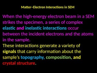
Matter–Electron Interactions inSEM
When the high-energy electron beam in a SEM
strikes the specimen, a series of complex
elastic and inelastic interactions occur
between the incident electrons and the atoms
in the sample.
These interactions generate a variety of
signals that carry information about the
sample’s topography, composition, and
crystal structure.
11.
1. Interaction Volume
Theregion inside the specimen
where electrons interact with
matter is called the interaction
volume.
Its size and shape depend on:
Accelerating voltage (higher
voltage → deeper
penetration)
Atomic number (Z) of the
material (higher Z → smaller
volume)
Density of the sample
Typically, the interaction
depth ranges from a few nm
to a few µm.
For light elements (e.g.,
carbon): up to ~2 µm
For heavy elements (e.g.,
gold): <100 nm
12.
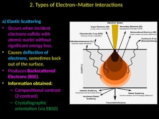
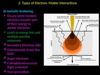
2. Types ofElectron–Matter Interactions
a) Elastic Scattering
• Occurs when incident
electrons collide with
atomic nuclei without
significant energy loss.
• Causes deflection of
electrons, sometimes back
out of the surface.
• Produces Backscattered
Electrons (BSE).
• Information obtained:
– Compositional contrast
(Z-contrast)
– Crystallographic
orientation (via EBSD)
13.
2. Types ofElectron–Matter Interactions
b) Inelastic Scattering
Occurs when incident
electrons transfer part
of their energy to
atomic electrons.
Leads to energy loss and
multiple possible
emissions:
Secondary Electrons (SE)
Characteristic X-rays (for
EDX)
Auger electrons
Cathodoluminescence
(light emission)
Heat generation
14.
Sample Preparation
• Samplesmust be clean, dry, and electrically
conductive.
• Non-conductive samples are coated with thin
conductive layers (Au, Pt, C) using sputter coating.
• Cross-sections may be polished or fractured to reveal
internal structures.
• Samples are mounted on metal stubs using conductive
tape or adhesive.
• Avoid contamination, charging, and mechanical
damage.
15.
Secondary vs. BackscatteredElectrons
• Secondary Electrons (SE):
• - Low energy (<50 eV)
• - Generated near the surface
• - Provide high-resolution topographic contrast.
• Backscattered Electrons (BSE):
• Higher energy (>50 eV)
• - Originate from deeper regions
• - Provide compositional contrast (brighter regions =
heavier elements).
16.
Energy Dispersive X-raySpectroscopy
(EDX/EDS)
• Occurs when high-energy electrons knock out inner
shell electrons.
• Outer shell electrons fill the vacancy, emitting
characteristic X-rays.
• Each element emits X-rays with unique energies,
enabling elemental analysis.
• EDX detector measures X-ray energy to identify and
quantify elements.
• Useful for compositional mapping, line scans, and
point analysis.
17.
Applications of SEM
•Surface morphology and microstructure
analysis.
• Nanoparticle size, shape, and distribution
study.
• Corrosion and coating analysis.
• Biological sample imaging (with proper
preparation).
• Elemental mapping using EDX/EDS.
18.
Comparison: Optical Microscopevs. SEM
• Parameter | Optical Microscope | Scanning Electron
Microscope (SEM)
• -----------|-------------------|-------------------------------------
• Source | Visible light | Electron beam
• Resolution | ~200 nm | <1–10 nm
• Magnification | Up to ~2000x | Up to ~1,000,000x
• Depth of Field | Shallow | Very large
• Image Type | Color, 2D | Grayscale, pseudo-3D
• Sample Type | Transparent or thin | Conductive or coated
19.
Summary
• • SEMprovides high-resolution imaging and
compositional information.
• • Combines multiple detection modes (SE, BSE,
EDX) for versatile analysis.
• • Essential in research and industry for
characterizing nanomaterials, surfaces, and
interfaces.
• • Continuous advances (like low-vacuum and
cryo-SEM) broaden its applications further.


![SEM_Group_2_ppt[1]..pptxtttttttttttttttt](https://cdn.slidesharecdn.com/ss_thumbnails/semgroup2ppt1-250821082712-4dd54452-thumbnail.jpg?width=640&height=640&fit=bounds)