Downloaded 948 times


![ELECTRON SOURCES
Anode [Hitachi S2300]](https://image.slidesharecdn.com/scanningelectronmicroscopymubbu-140116073649-phpapp01/85/Scanning-electron-microscopy-mubbu-10-320.jpg)


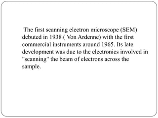
![Final Lens
Backscatter
Detector
Secondary
Detector
SEM Sample Chamber [AMRAY 1830] showing positions
of SE and BSE Detectors and the Final Lens](https://image.slidesharecdn.com/scanningelectronmicroscopymubbu-140116073649-phpapp01/85/Scanning-electron-microscopy-mubbu-13-320.jpg)
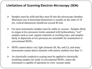
![Backscattered Electron
Generation
-SEM-BSE
-primary beam electrons
-high energy
-composition and topography
[specimen atomic number]](https://image.slidesharecdn.com/scanningelectronmicroscopymubbu-140116073649-phpapp01/85/Scanning-electron-microscopy-mubbu-14-320.jpg)
![SEM Imaging Modes
Secondary Electron
Generation
-SEM-SE
-sample electrons ejected by the
primary beam [green line]
-low energy
-surface detail & topography](https://image.slidesharecdn.com/scanningelectronmicroscopymubbu-140116073649-phpapp01/85/Scanning-electron-microscopy-mubbu-15-320.jpg)


This document provides an overview of scanning electron microscopy (SEM). It discusses how SEM works by using a beam of electrons to examine objects at a very fine scale, with greater resolving power than light microscopes. The first SEM debuted in 1938. SEM can provide information about a sample's topography, morphology, composition, and crystal structure. Diagrams show the major components of an SEM, including the electron gun and various detectors. Imaging modes like secondary electron and backscattered electron are described. Applications and limitations of SEM are also summarized.