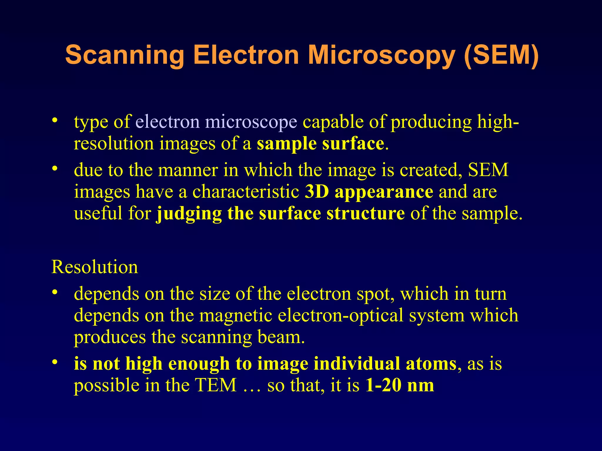
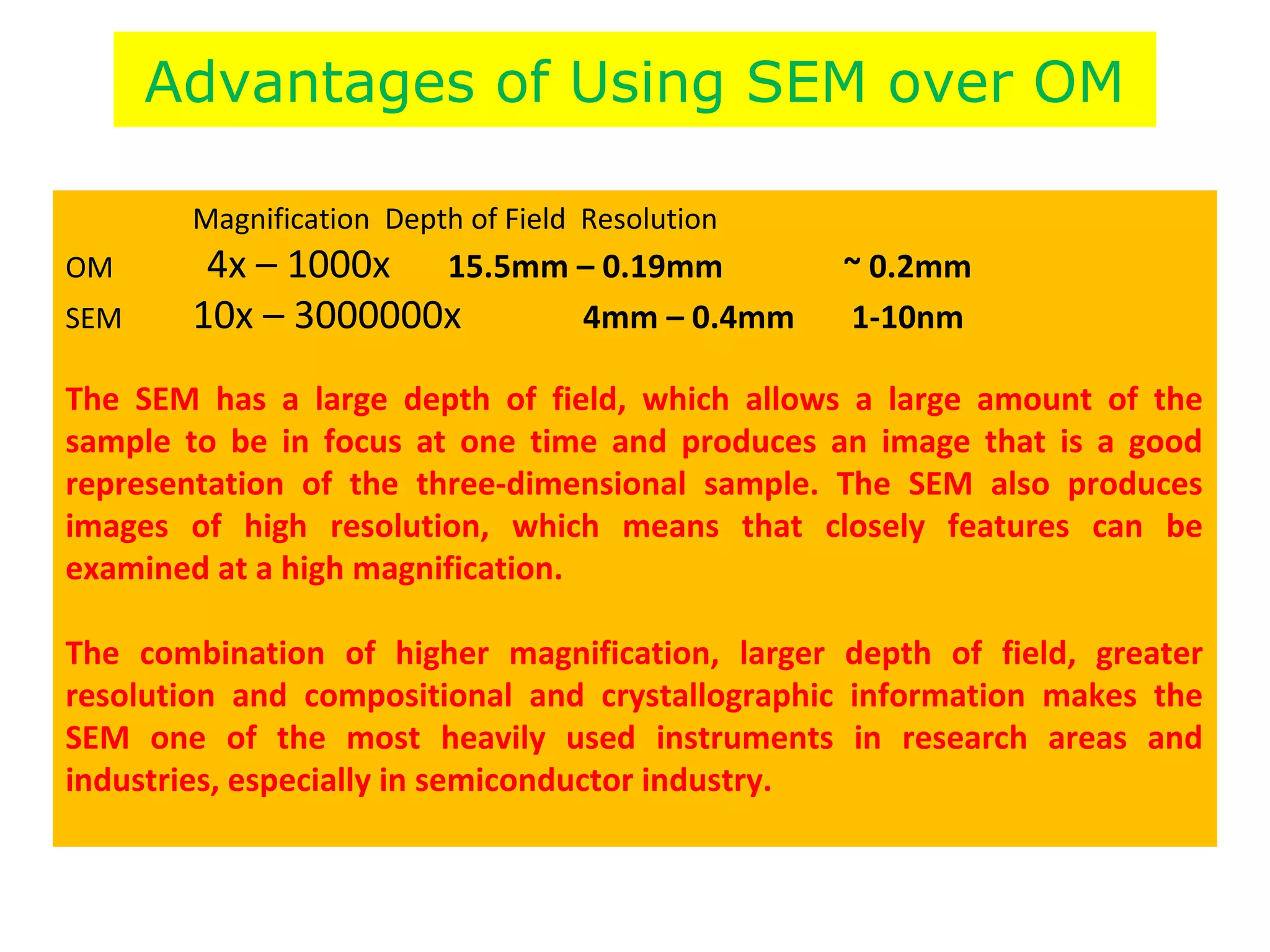
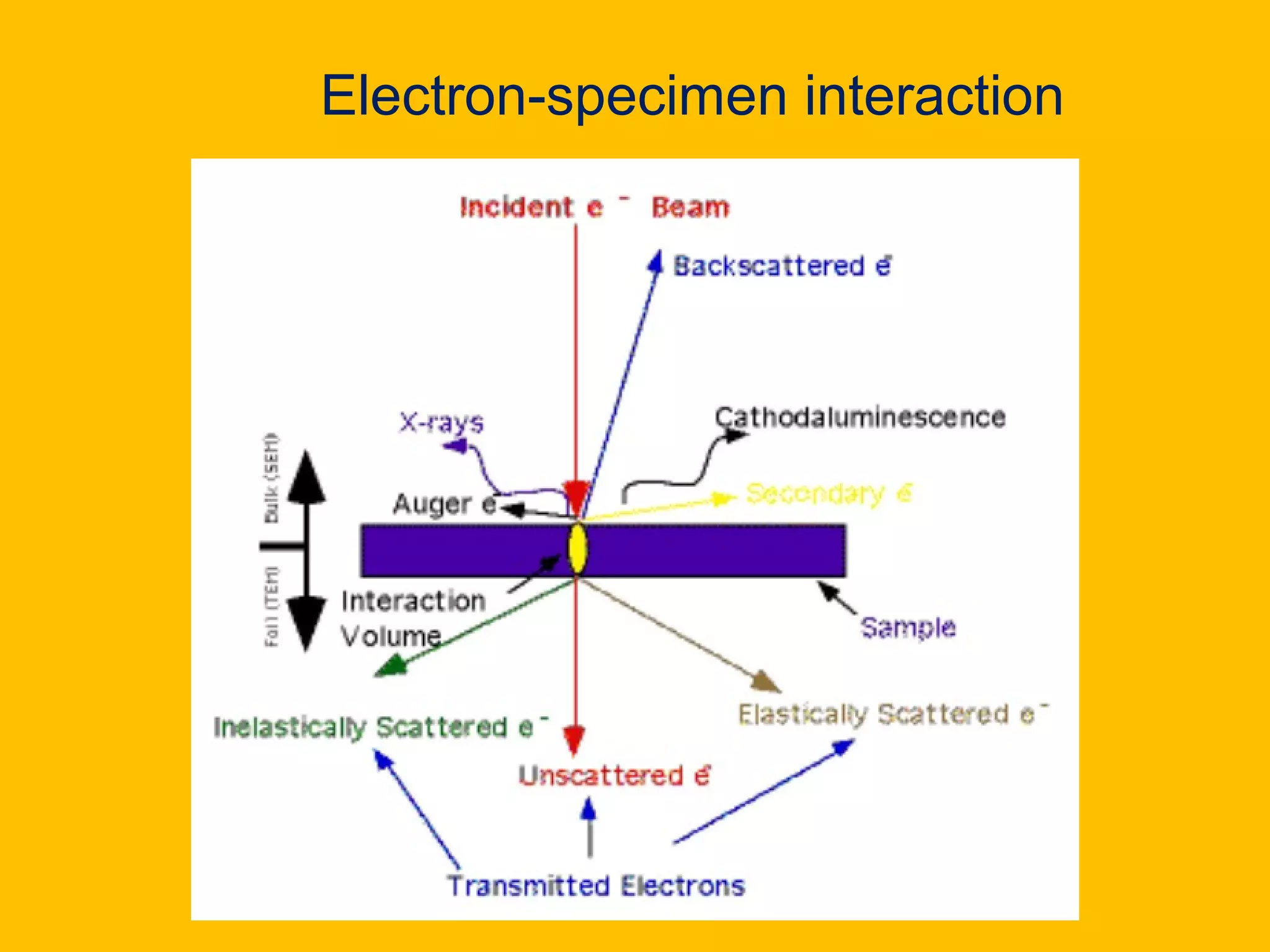
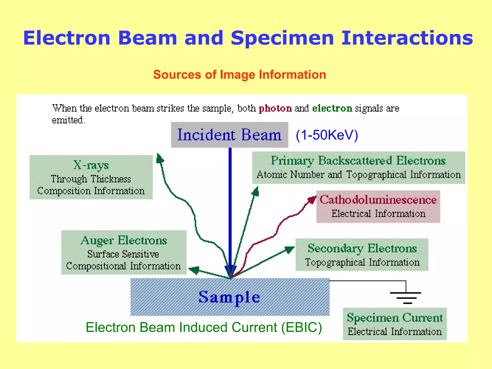
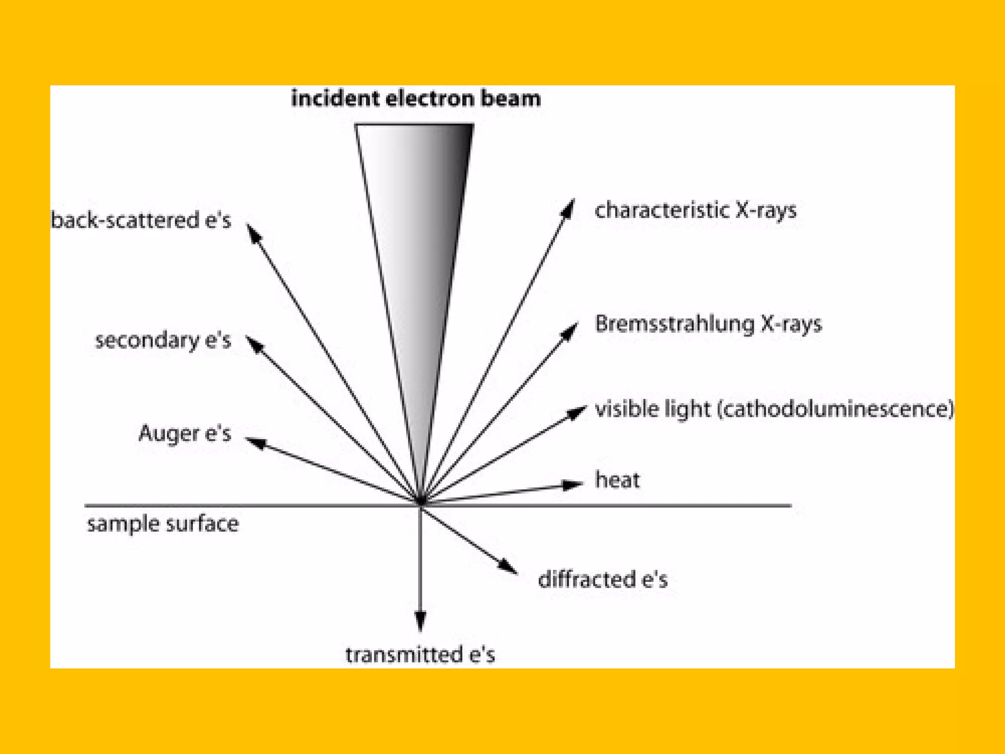
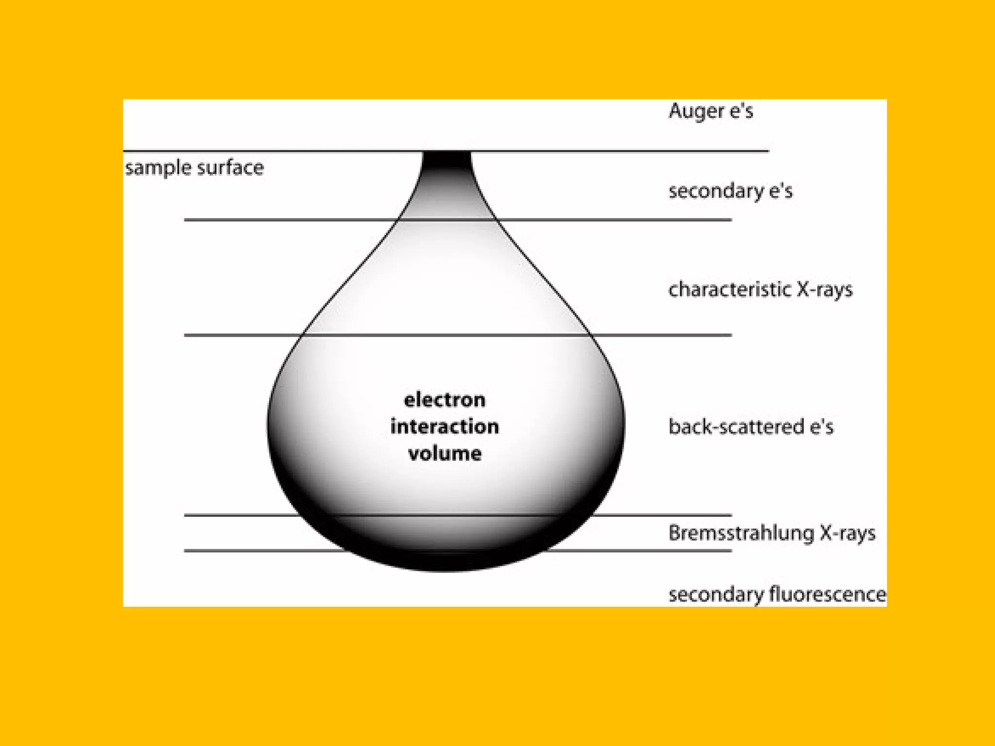
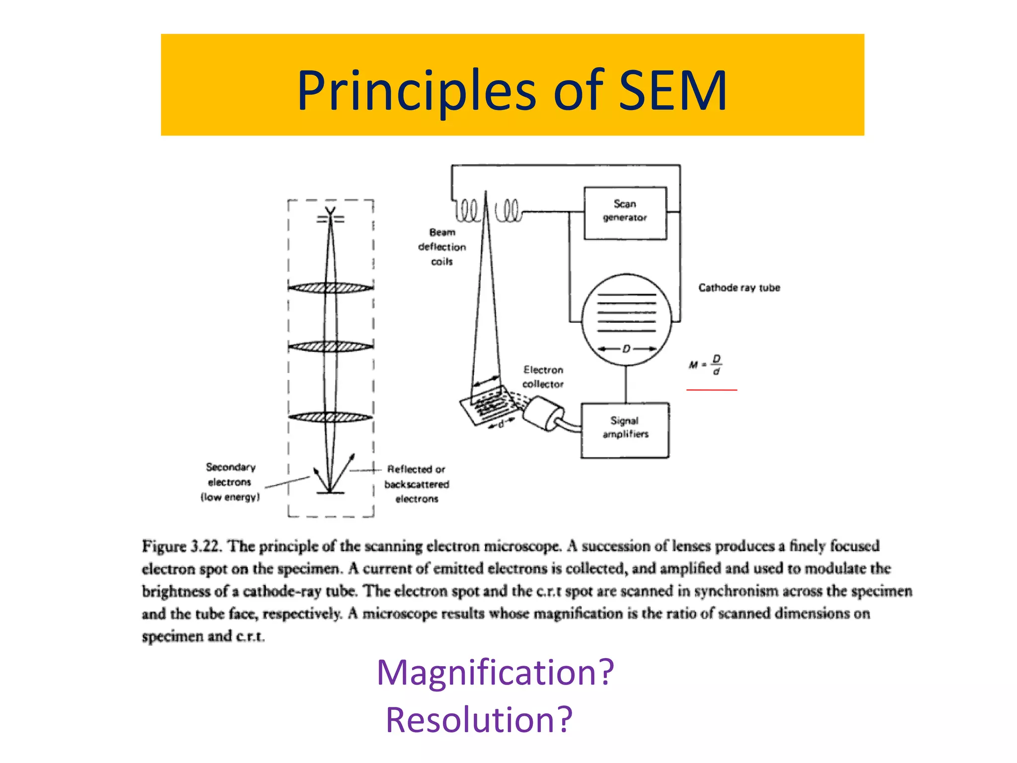
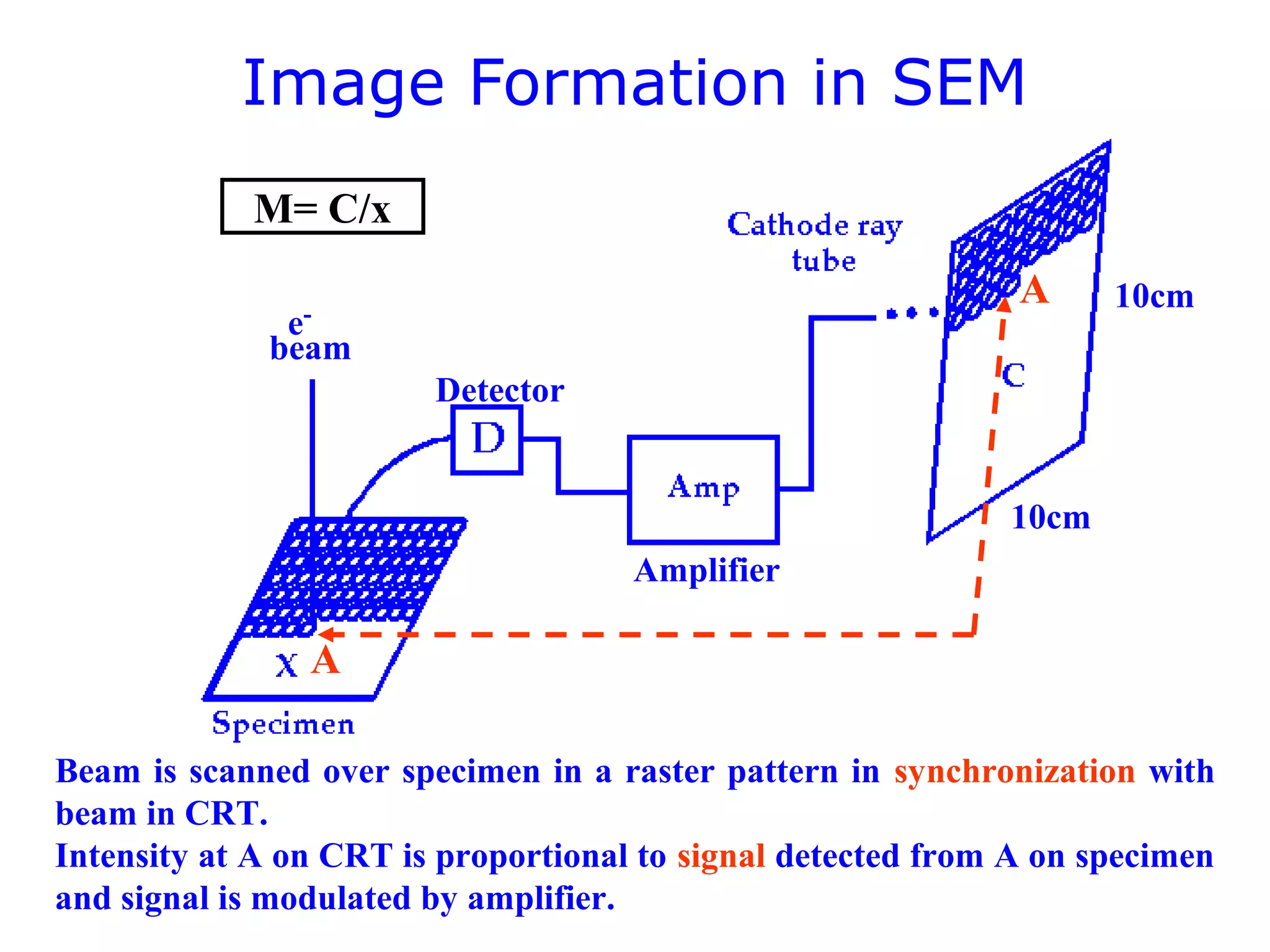
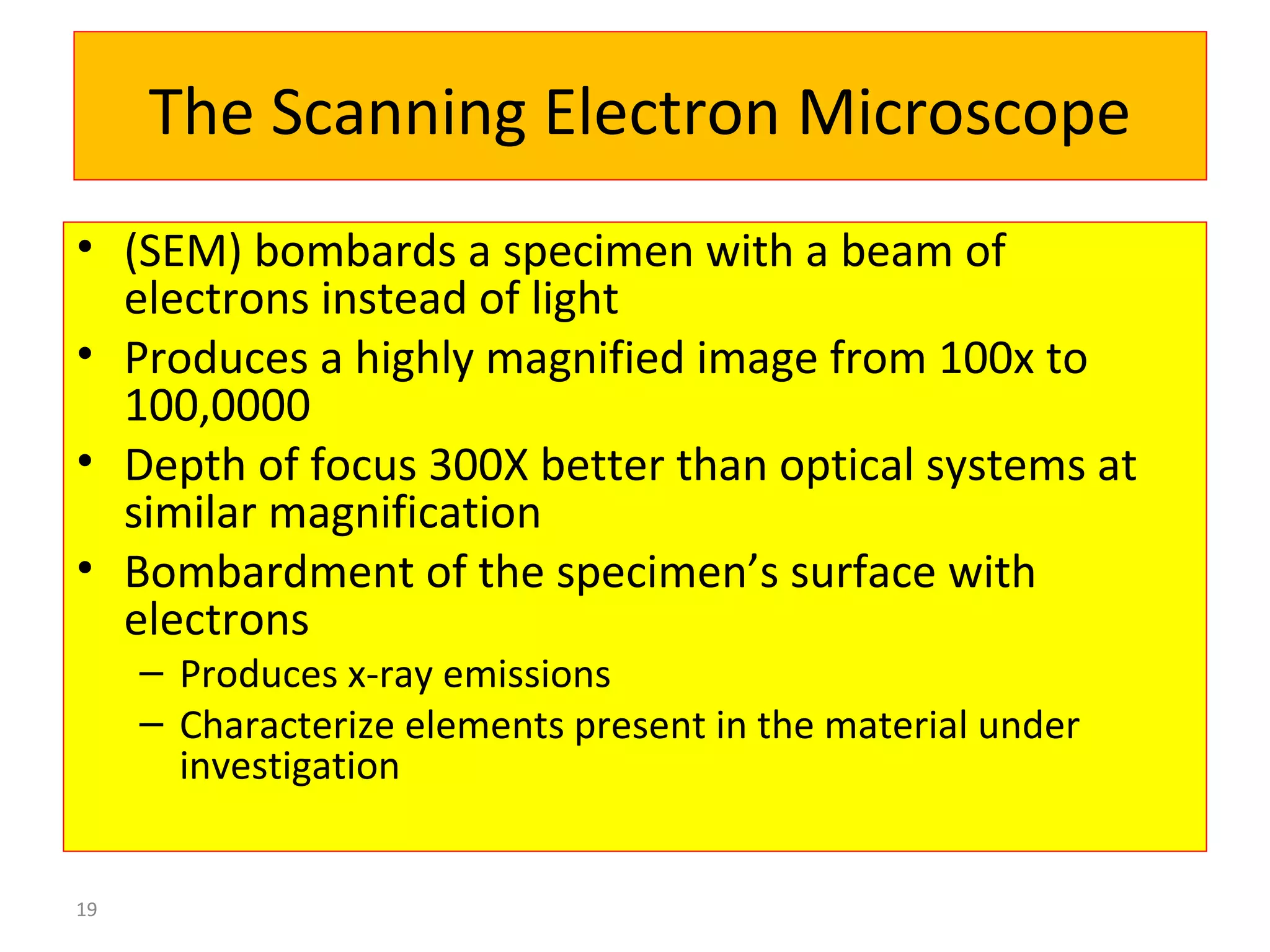
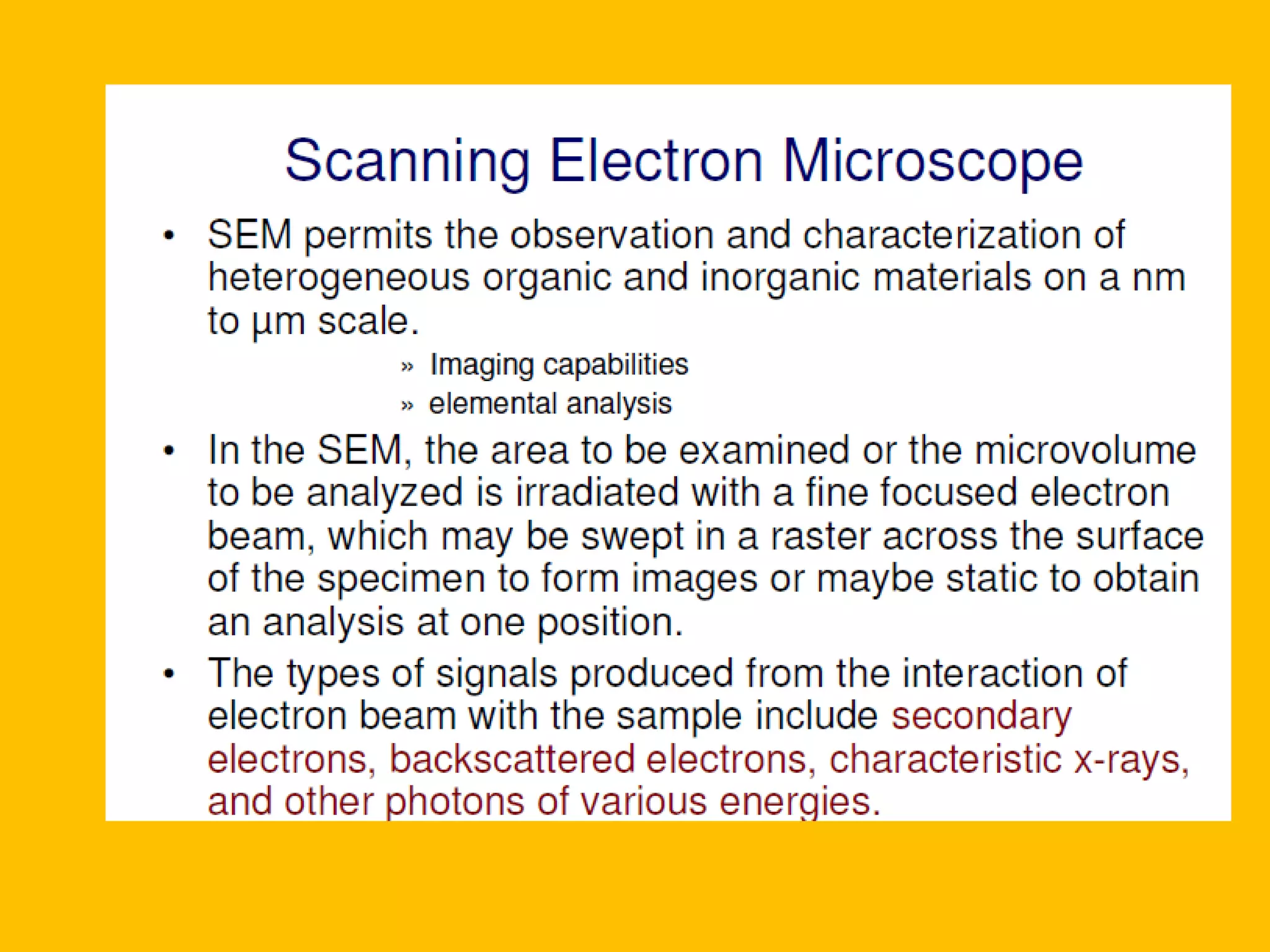
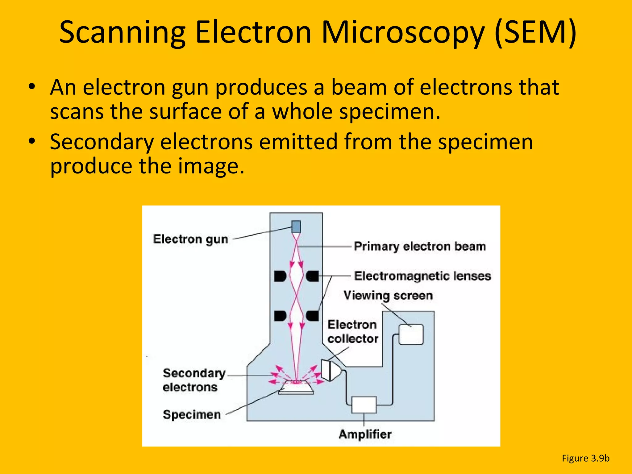
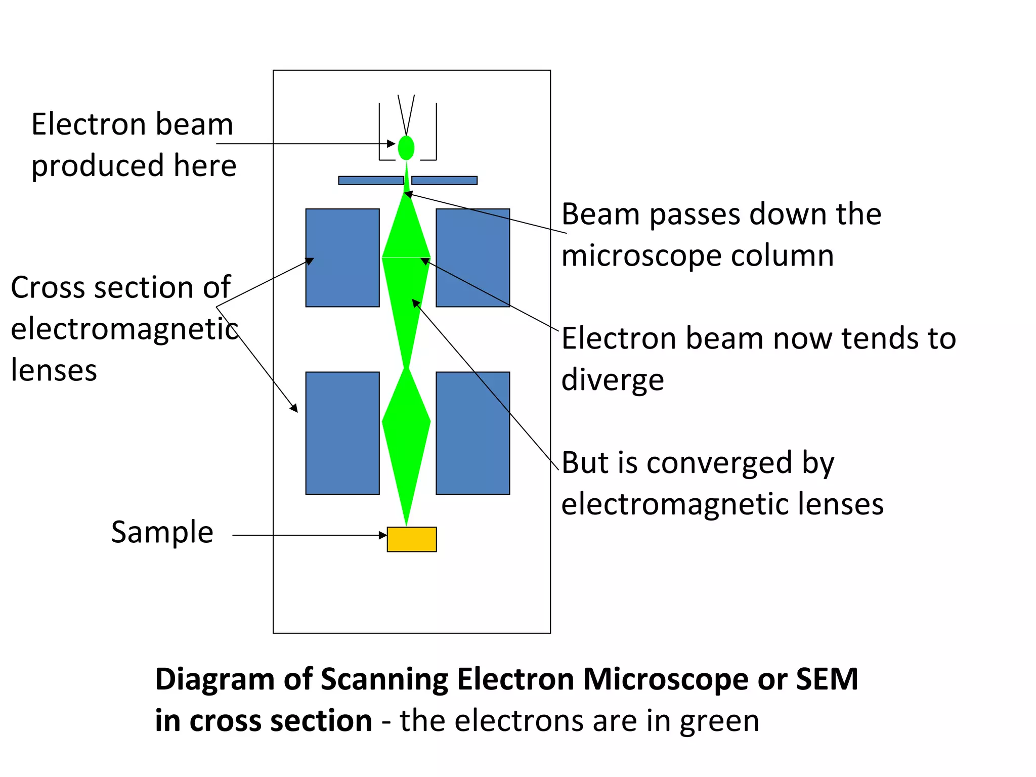
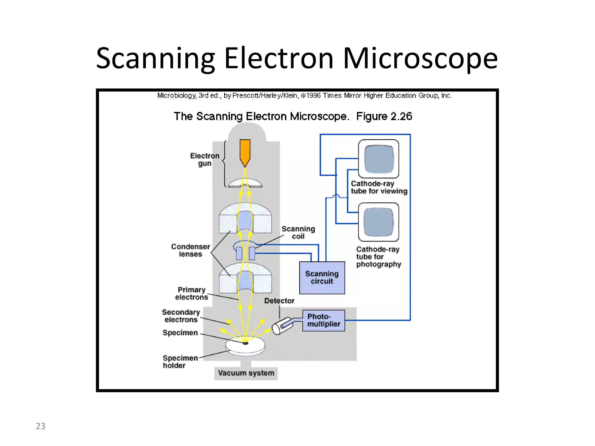
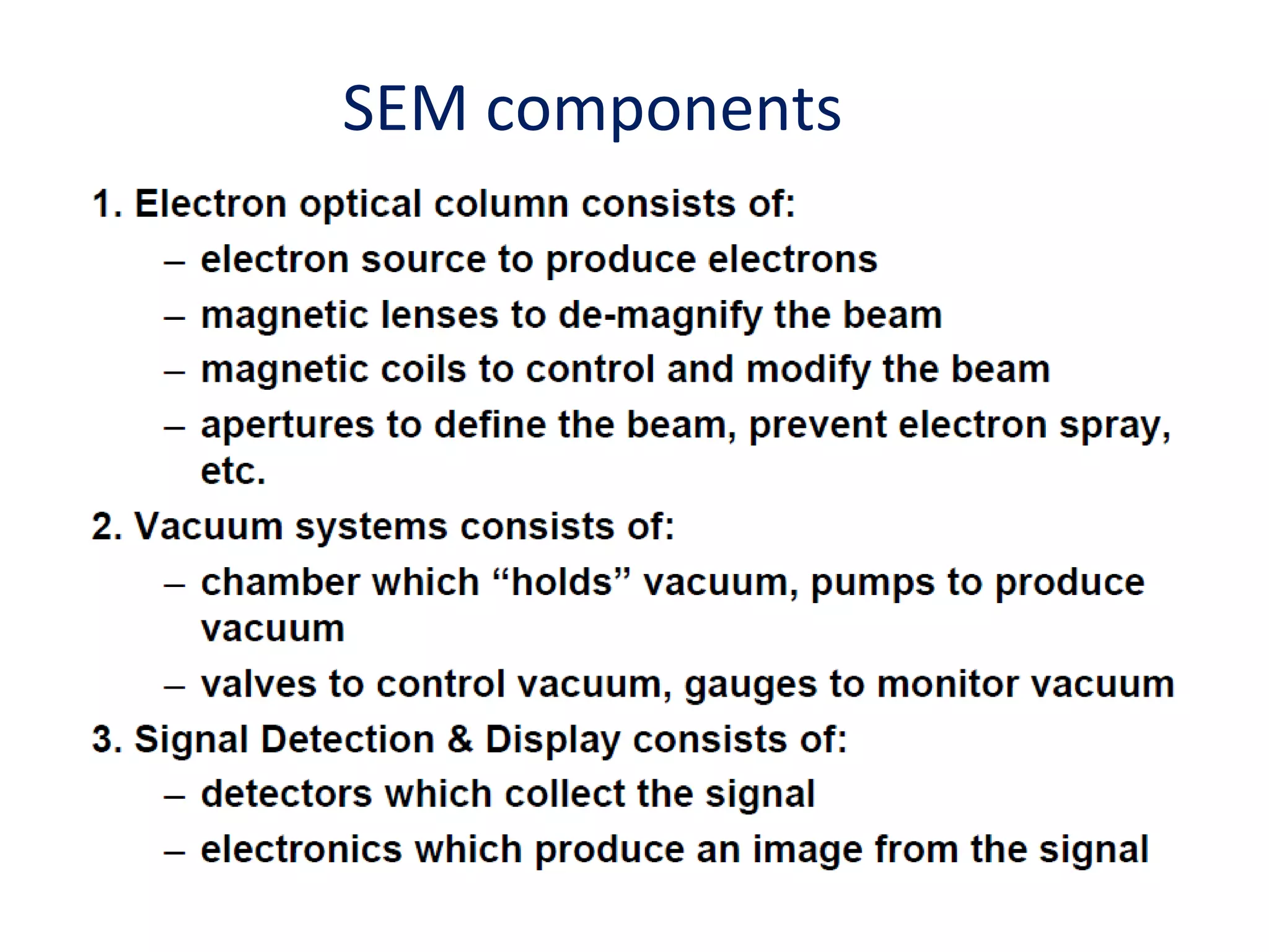
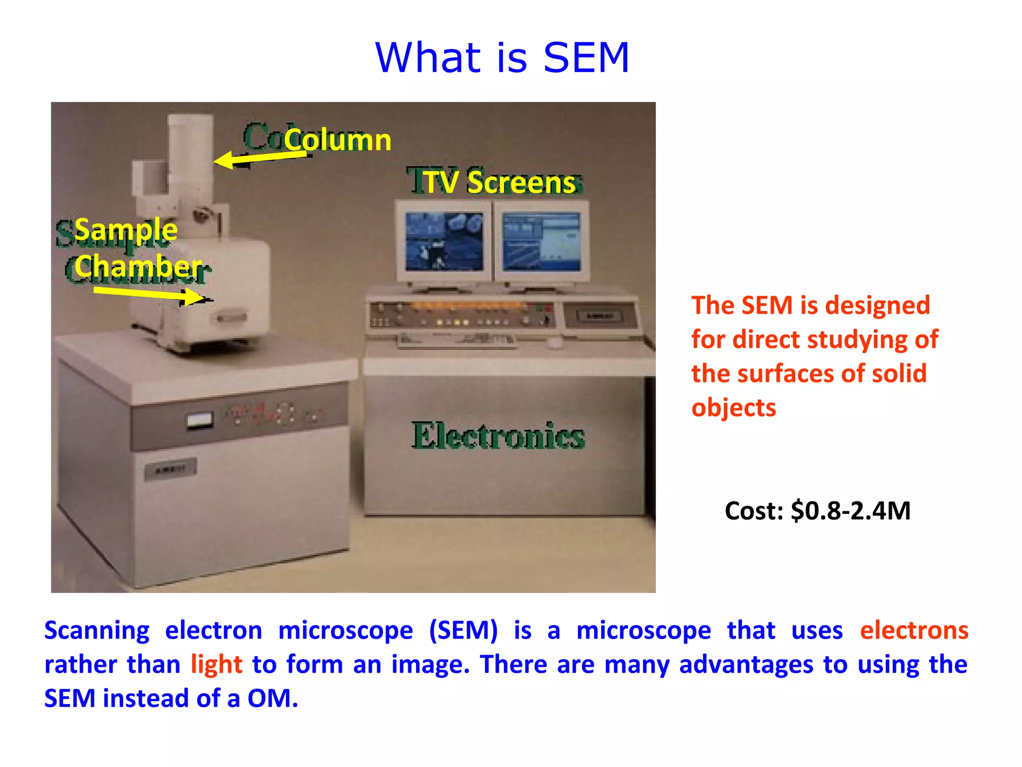
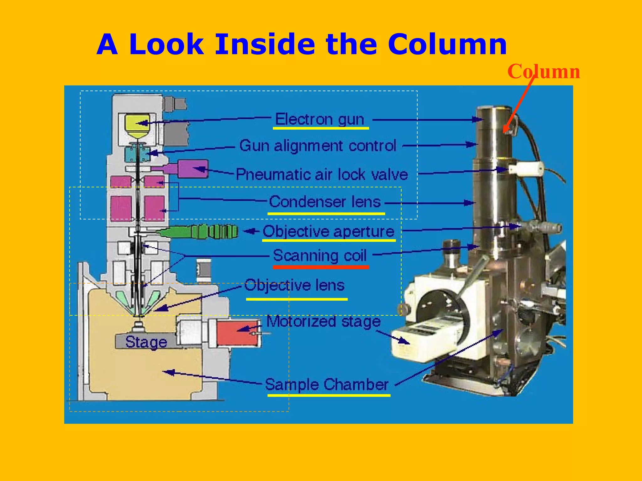
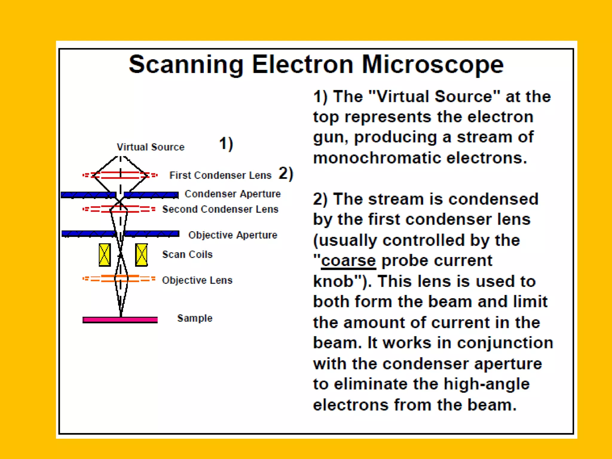
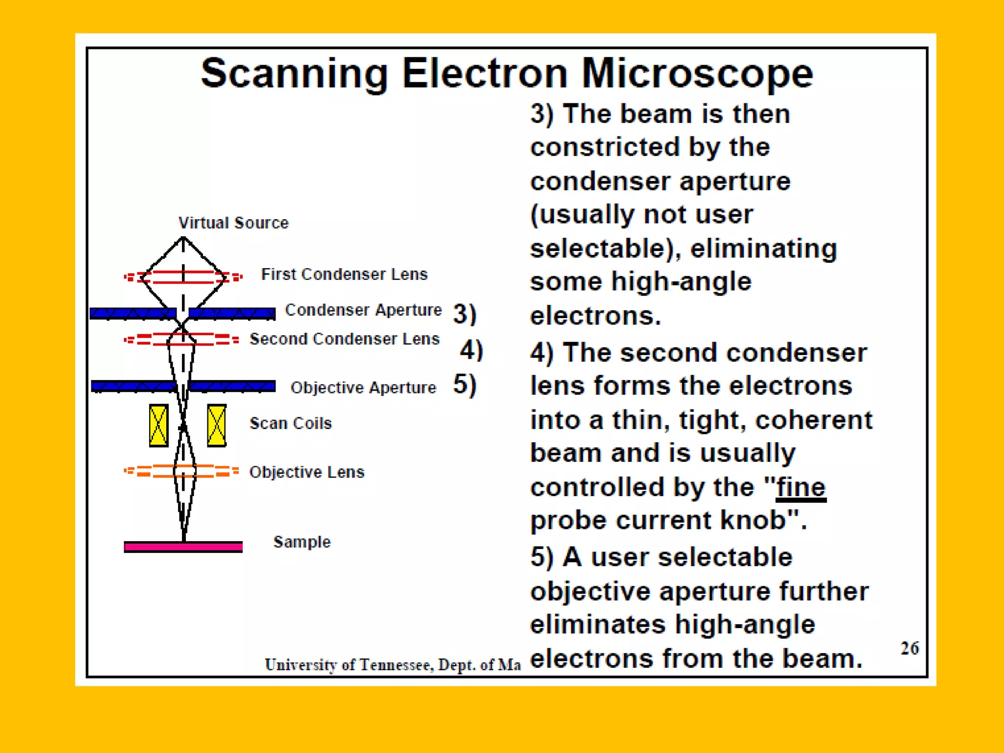
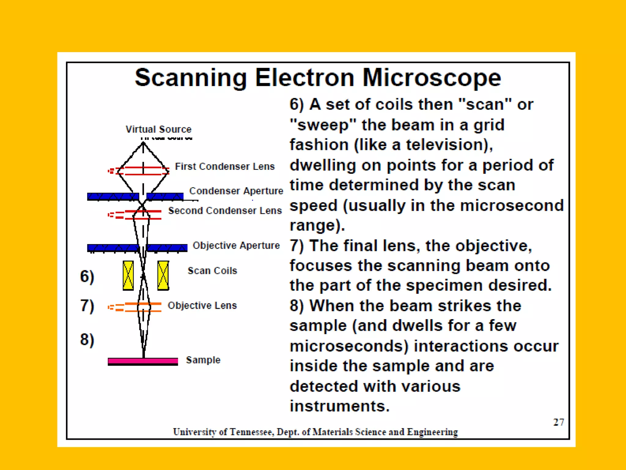
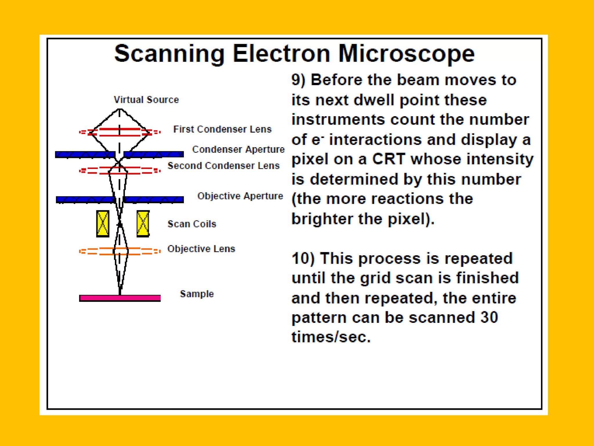
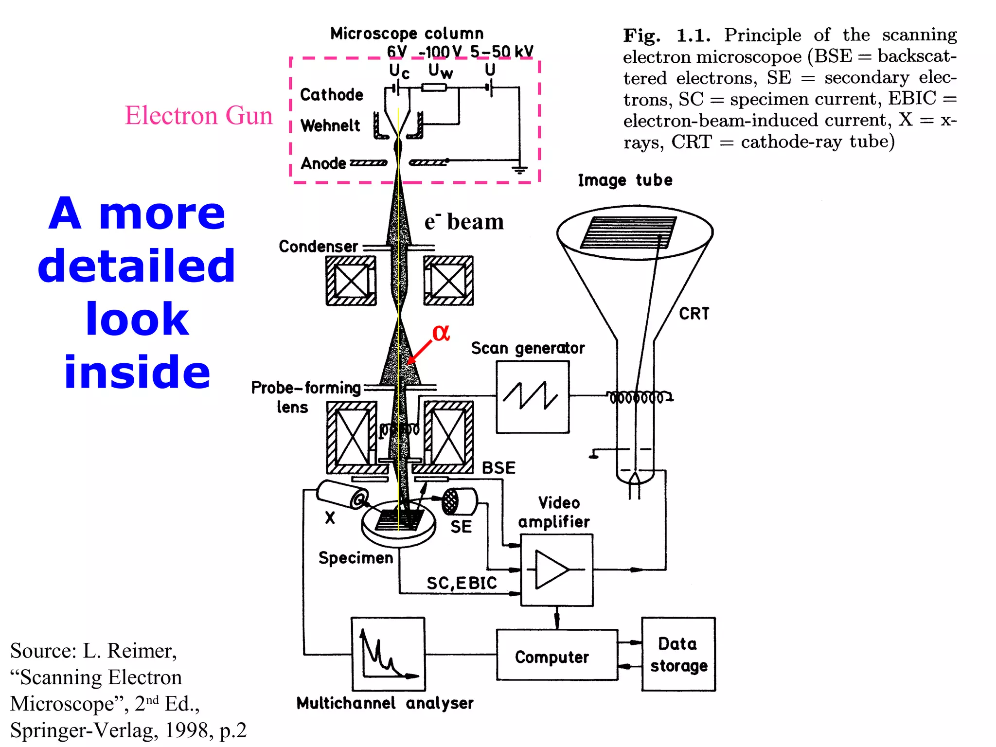
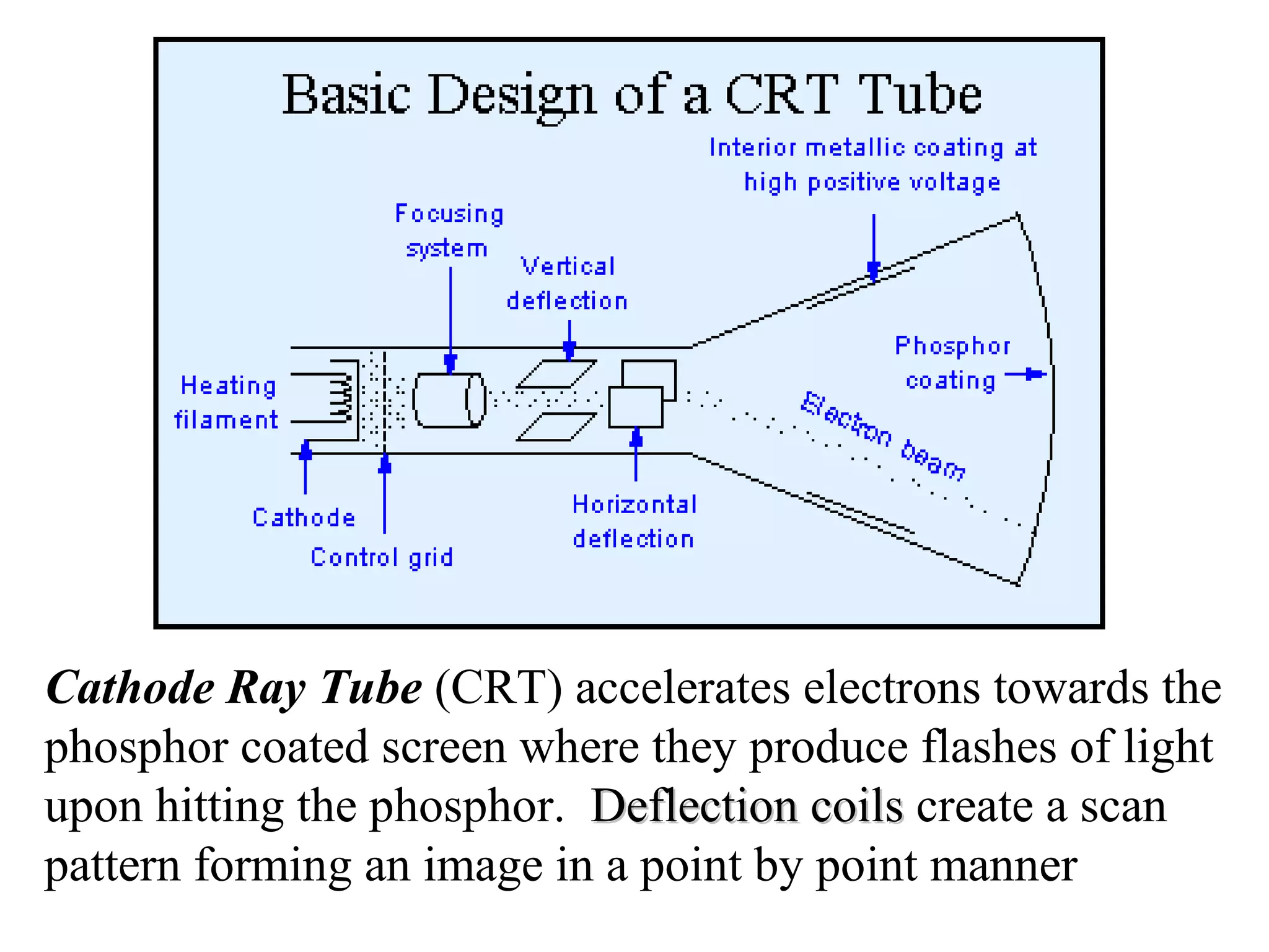
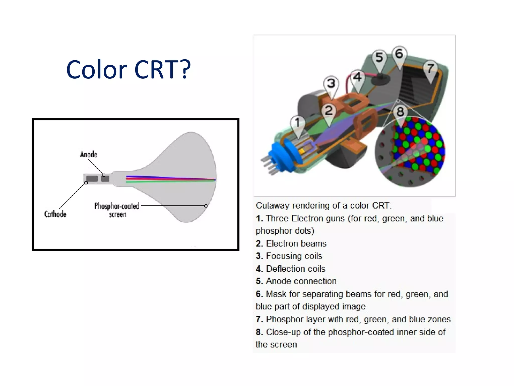
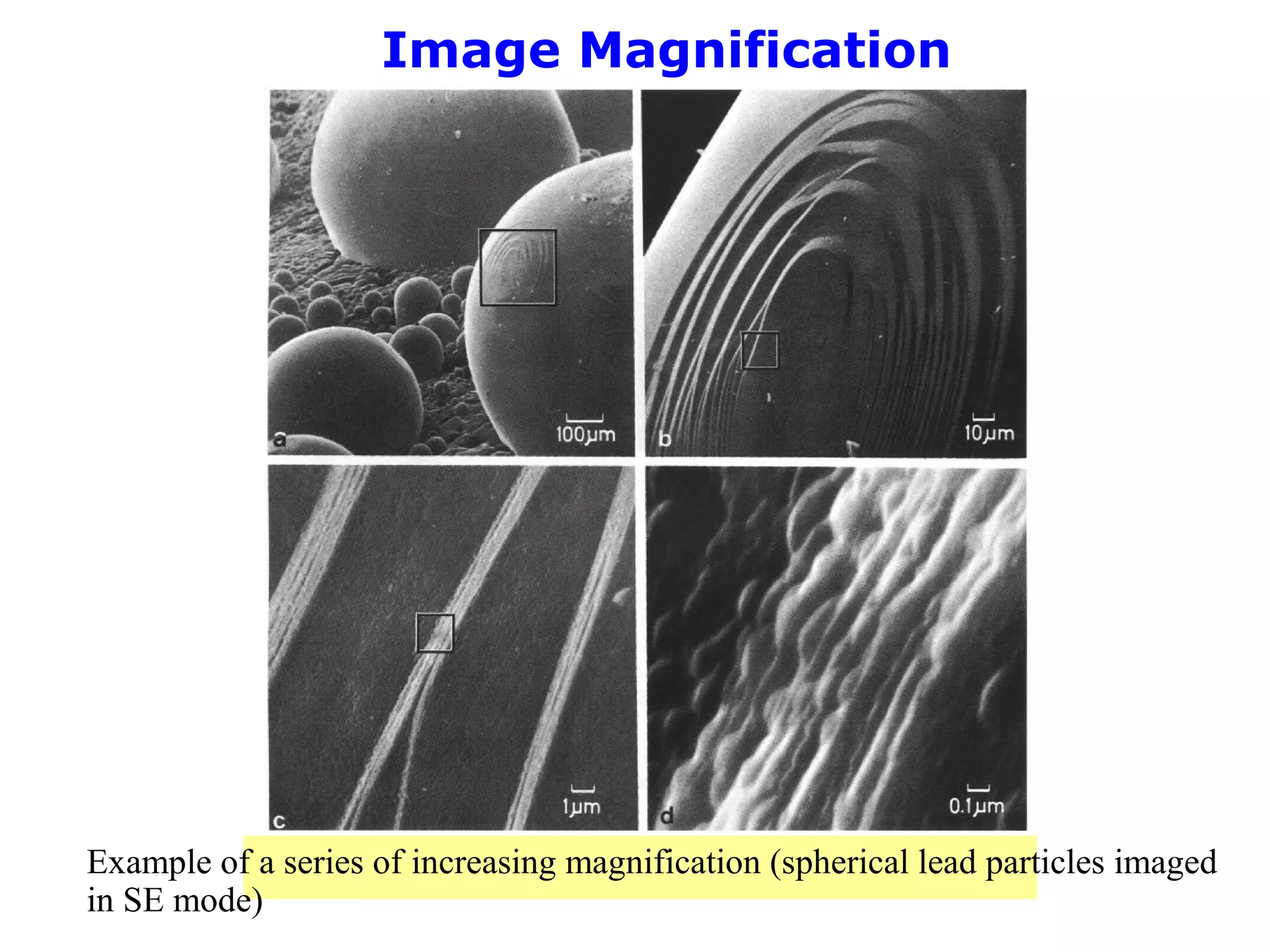
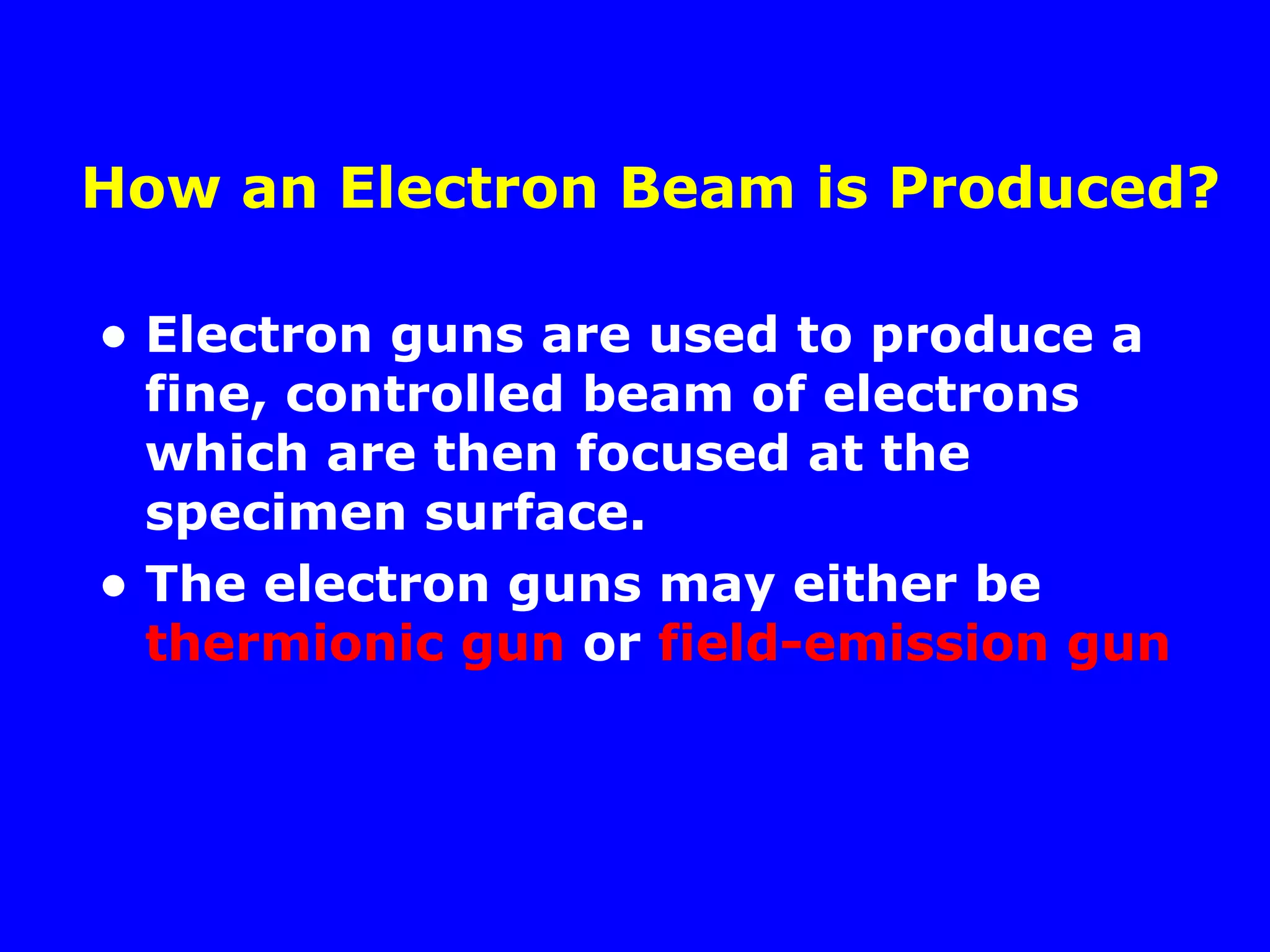
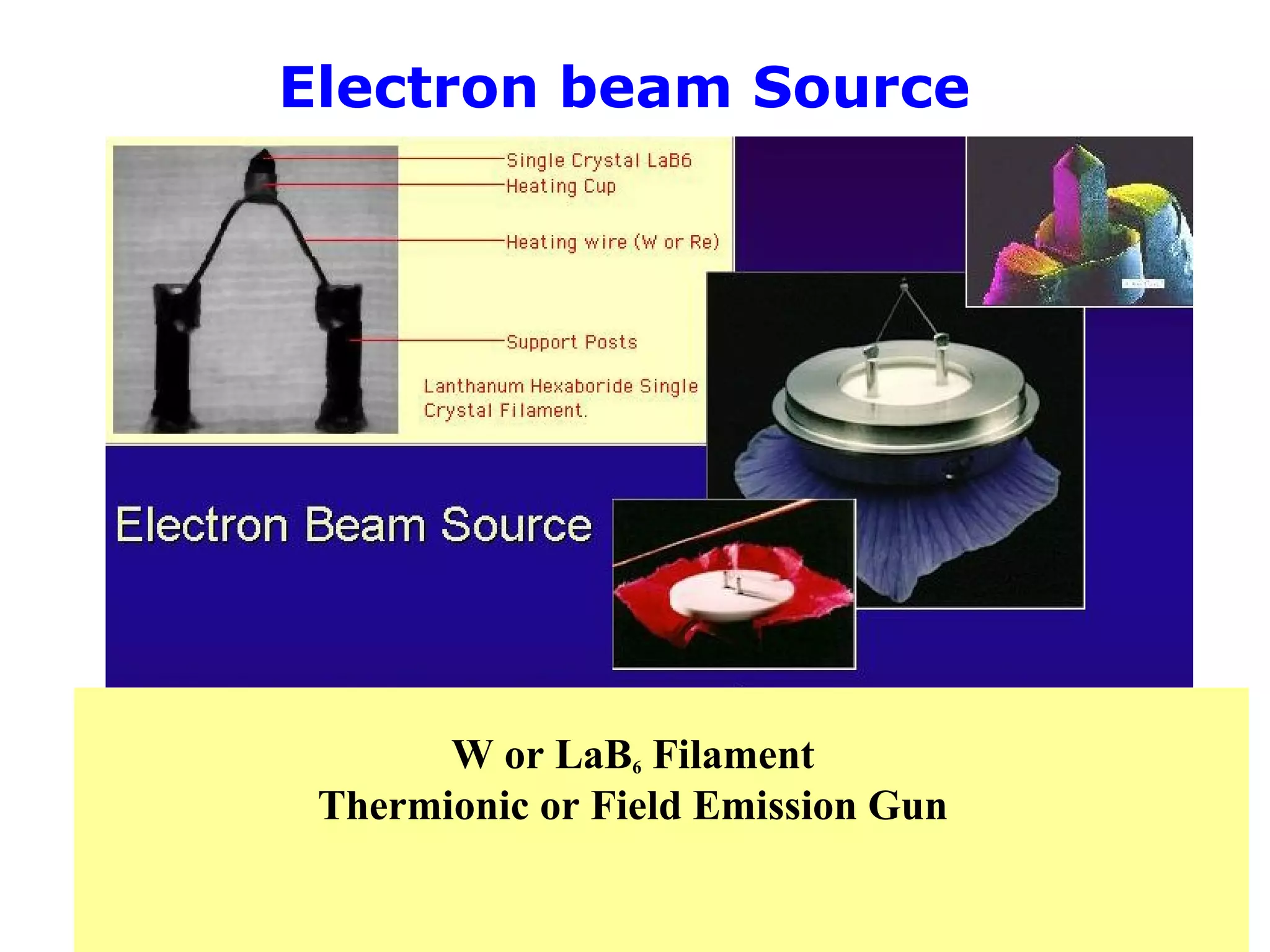
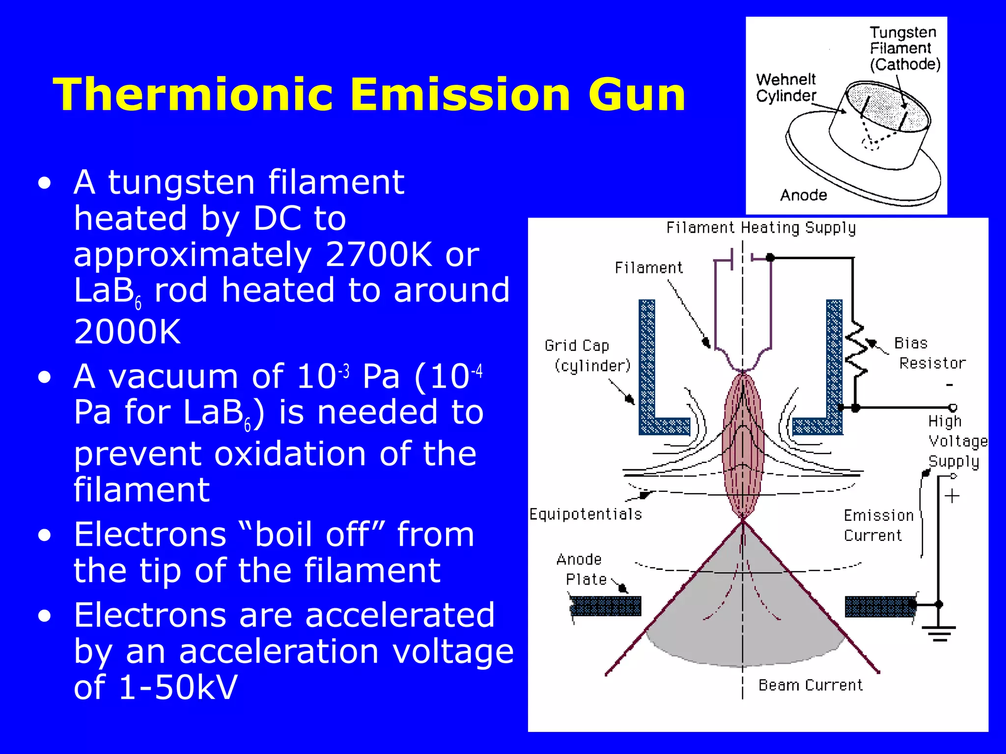
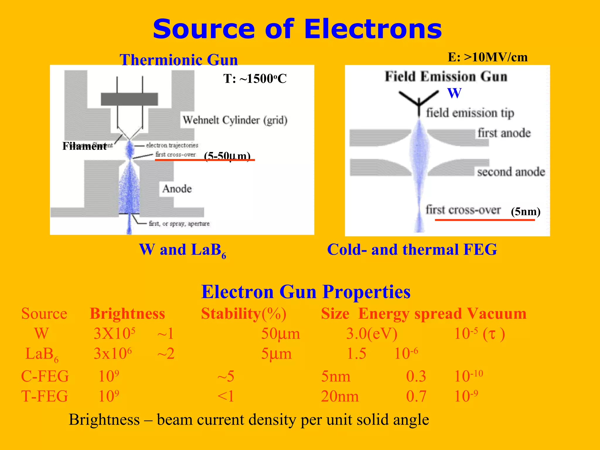
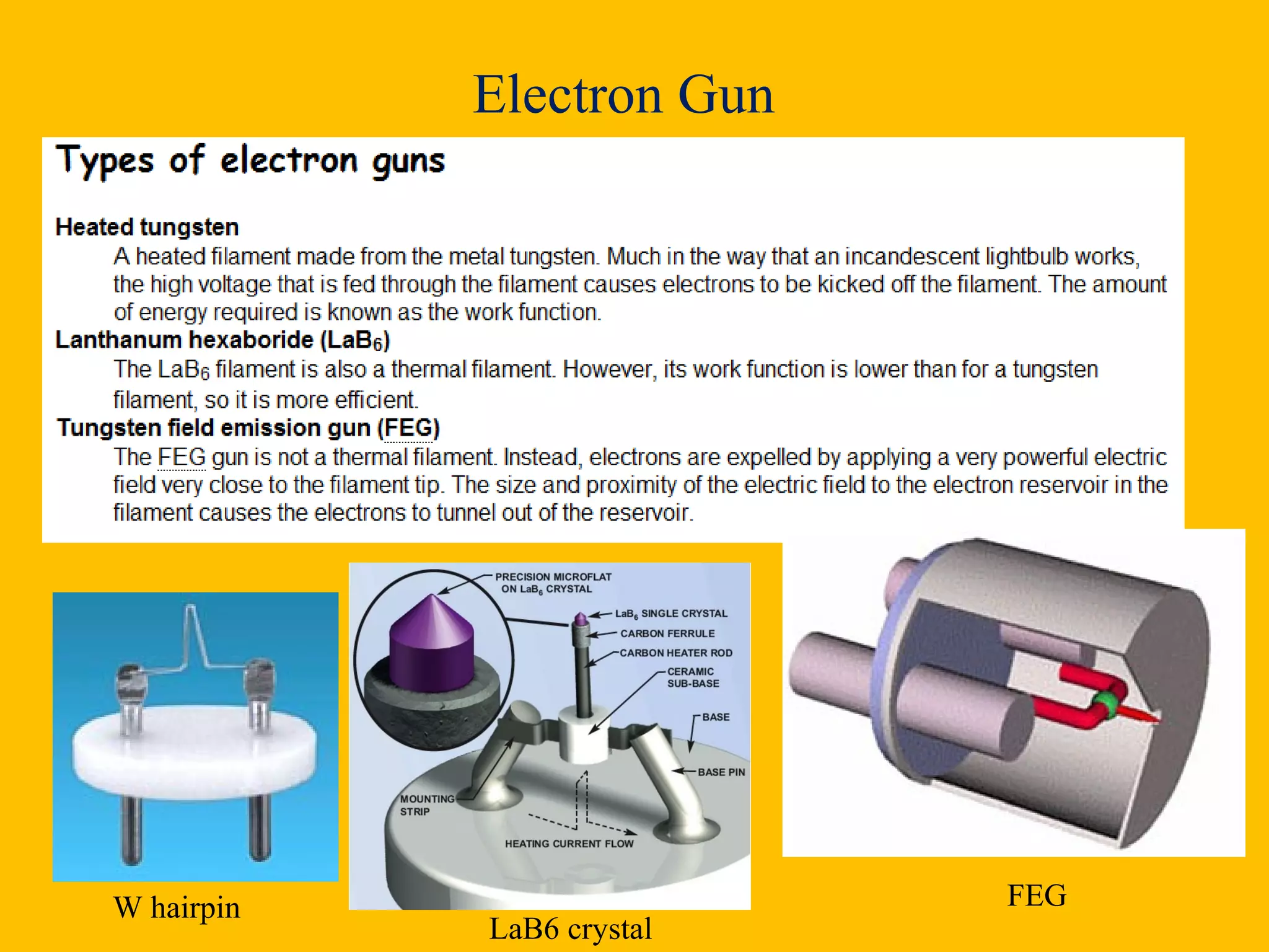
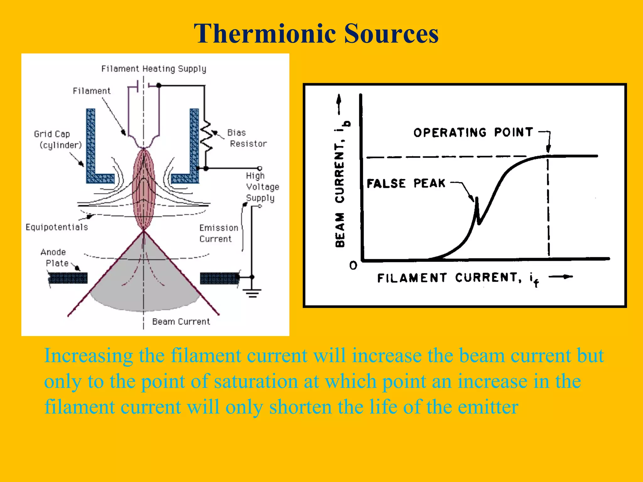
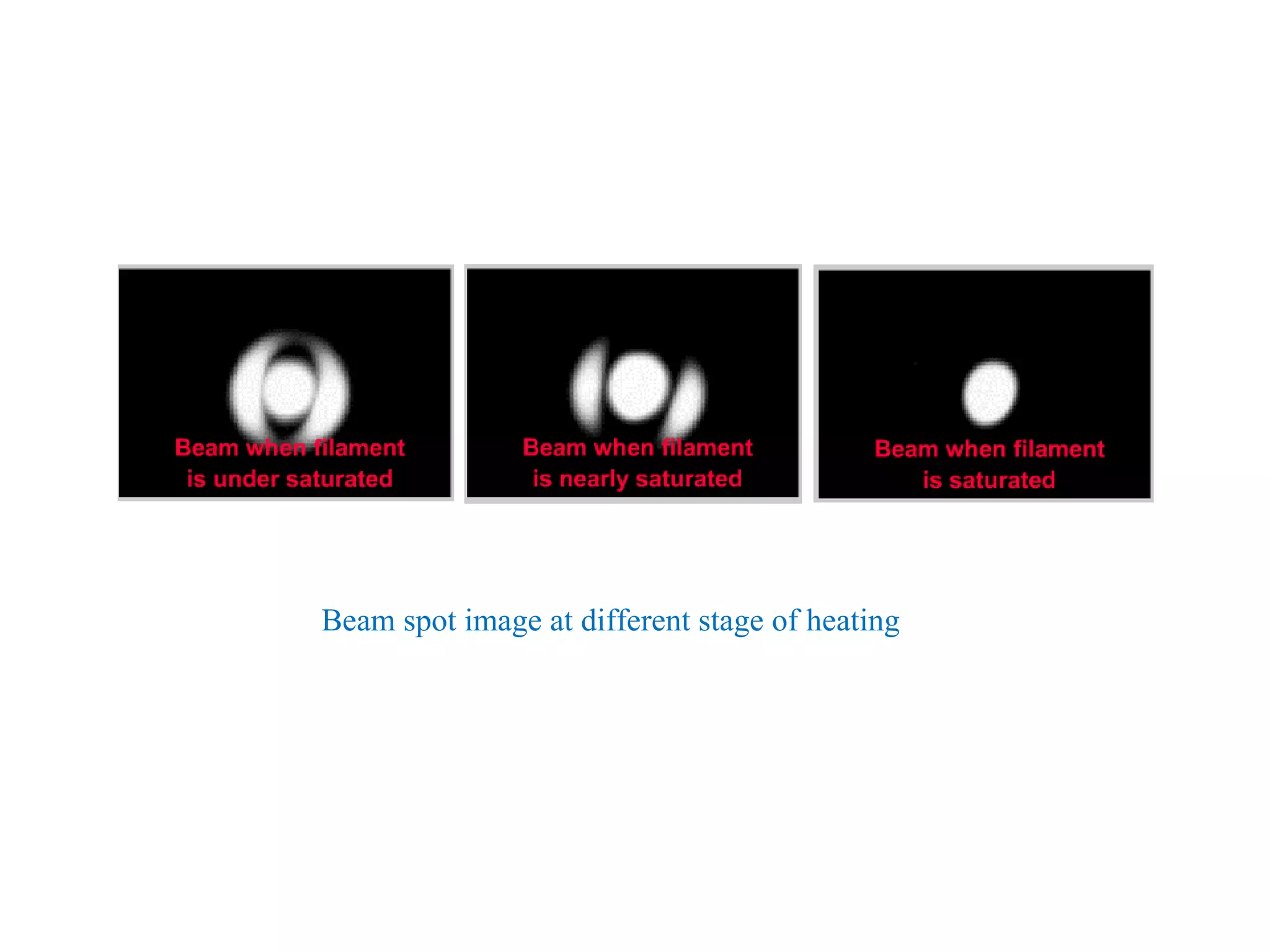
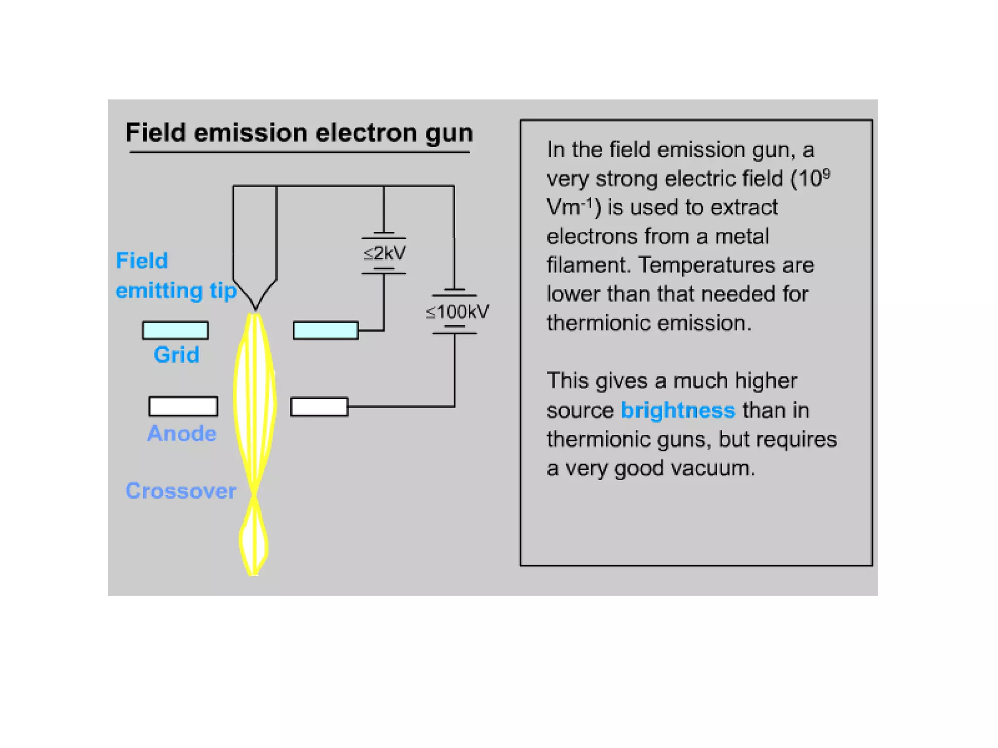
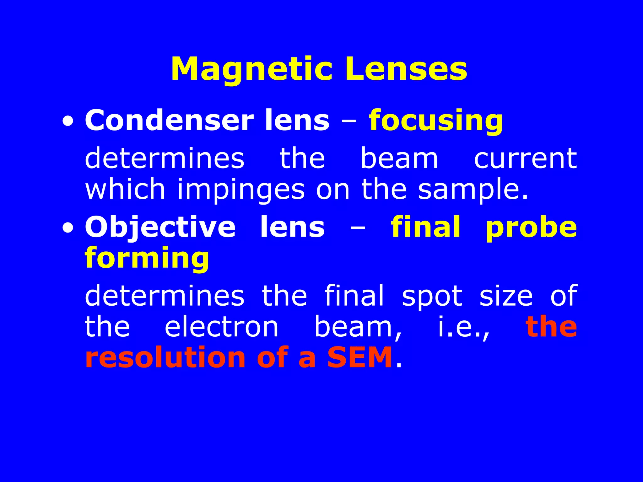
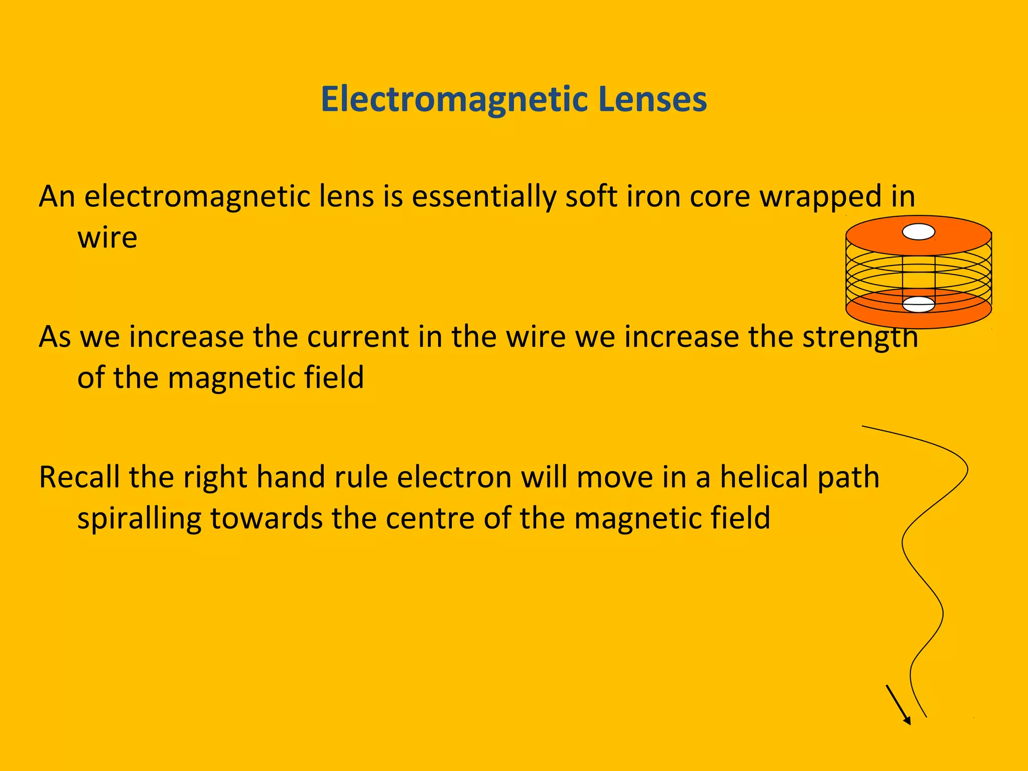
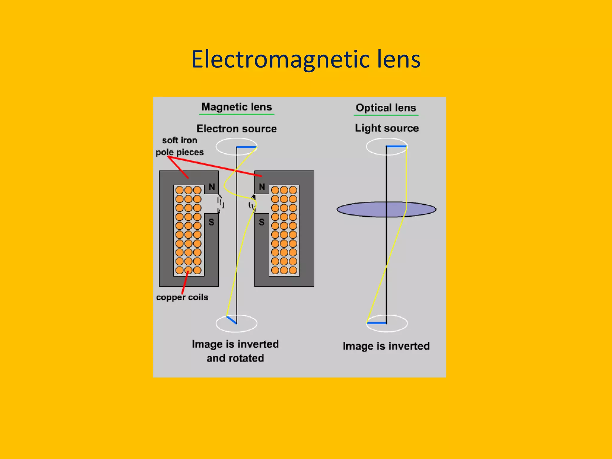
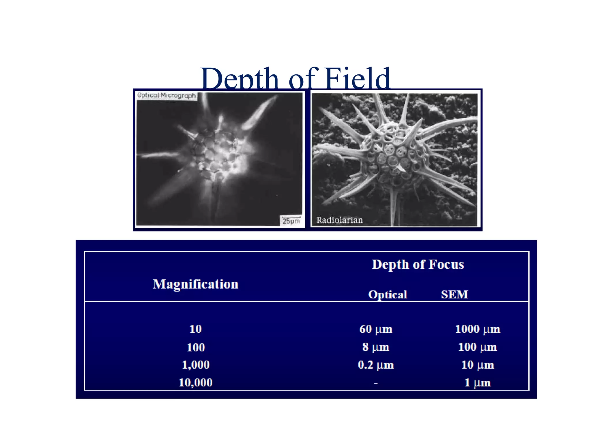
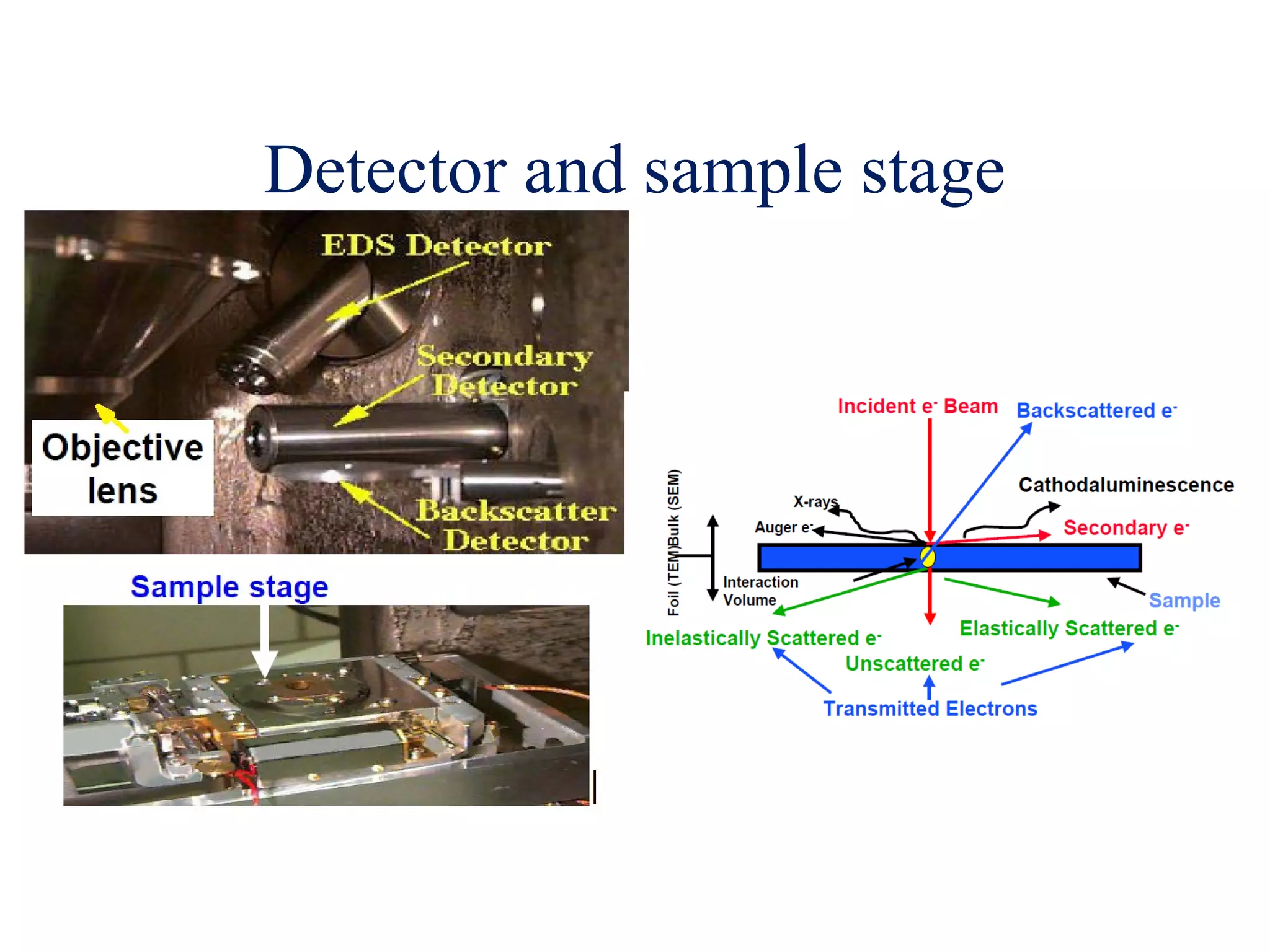
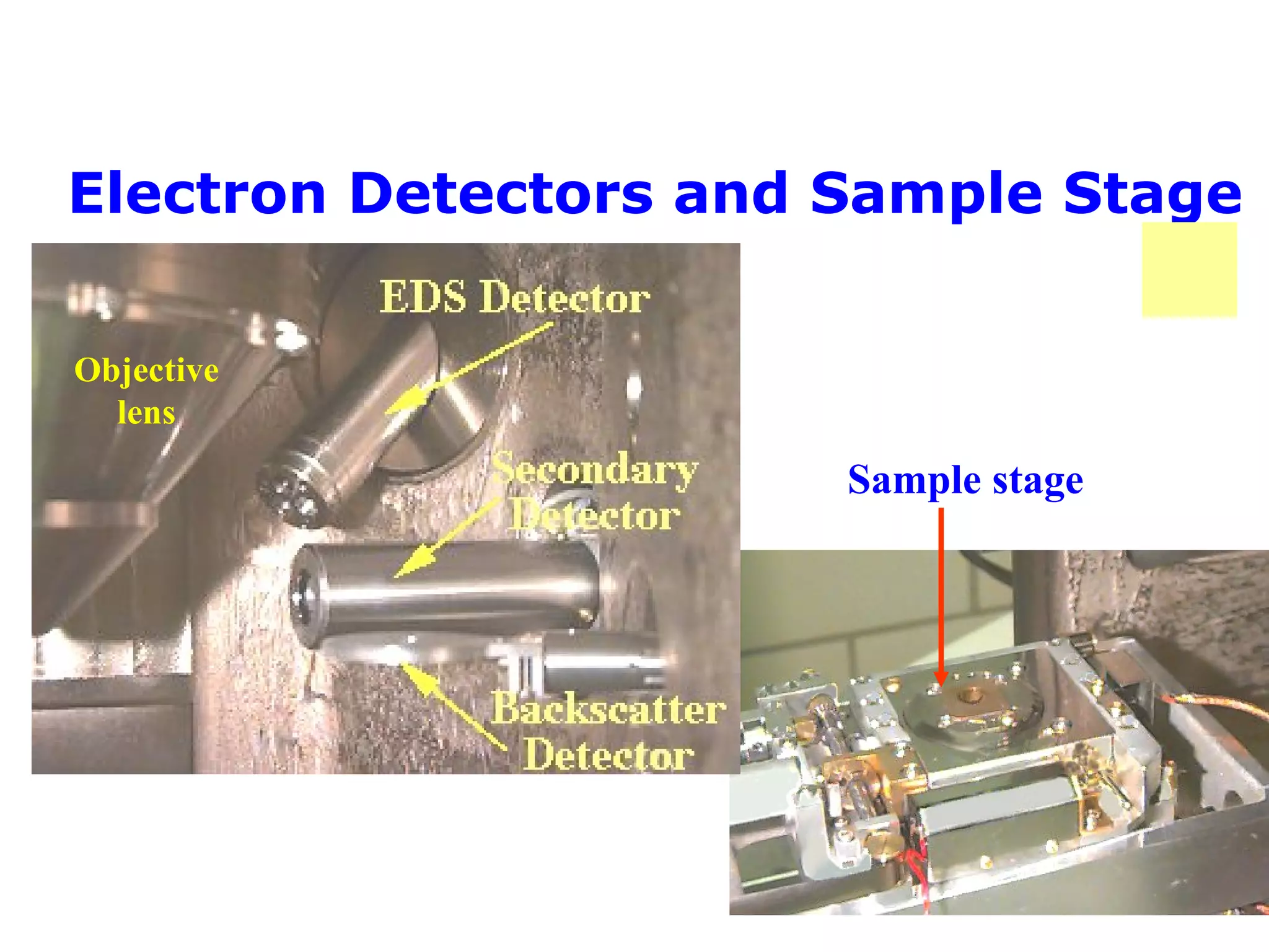
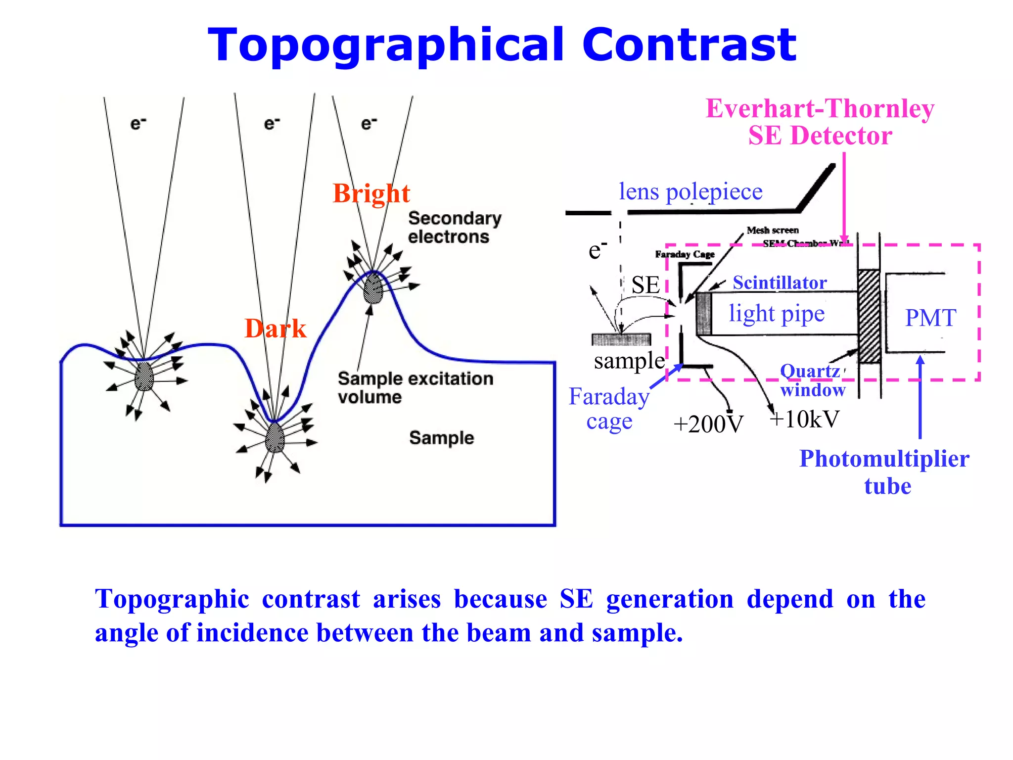
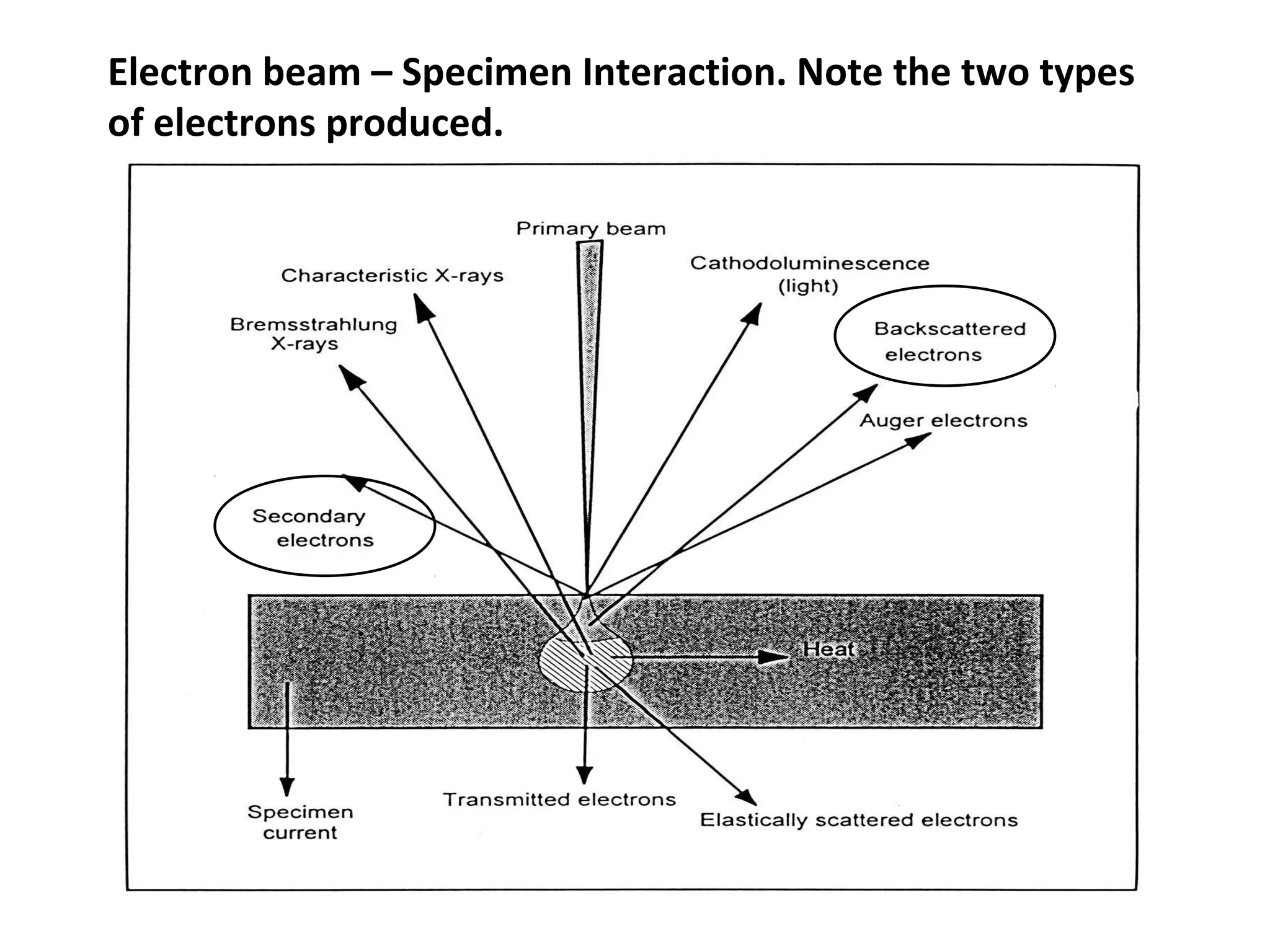
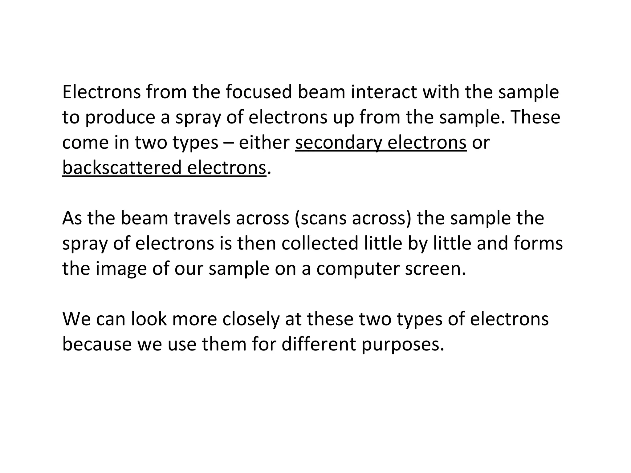
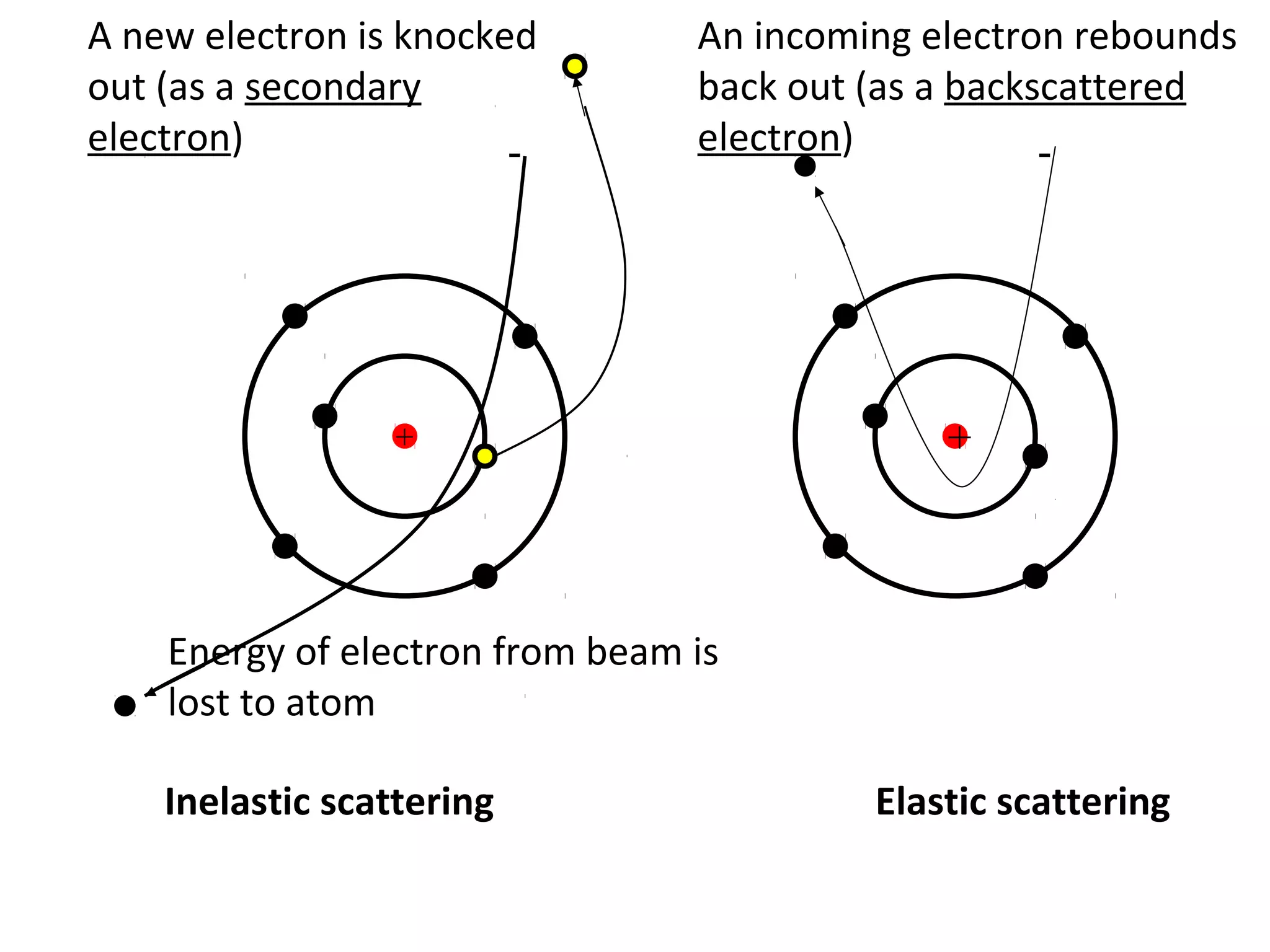
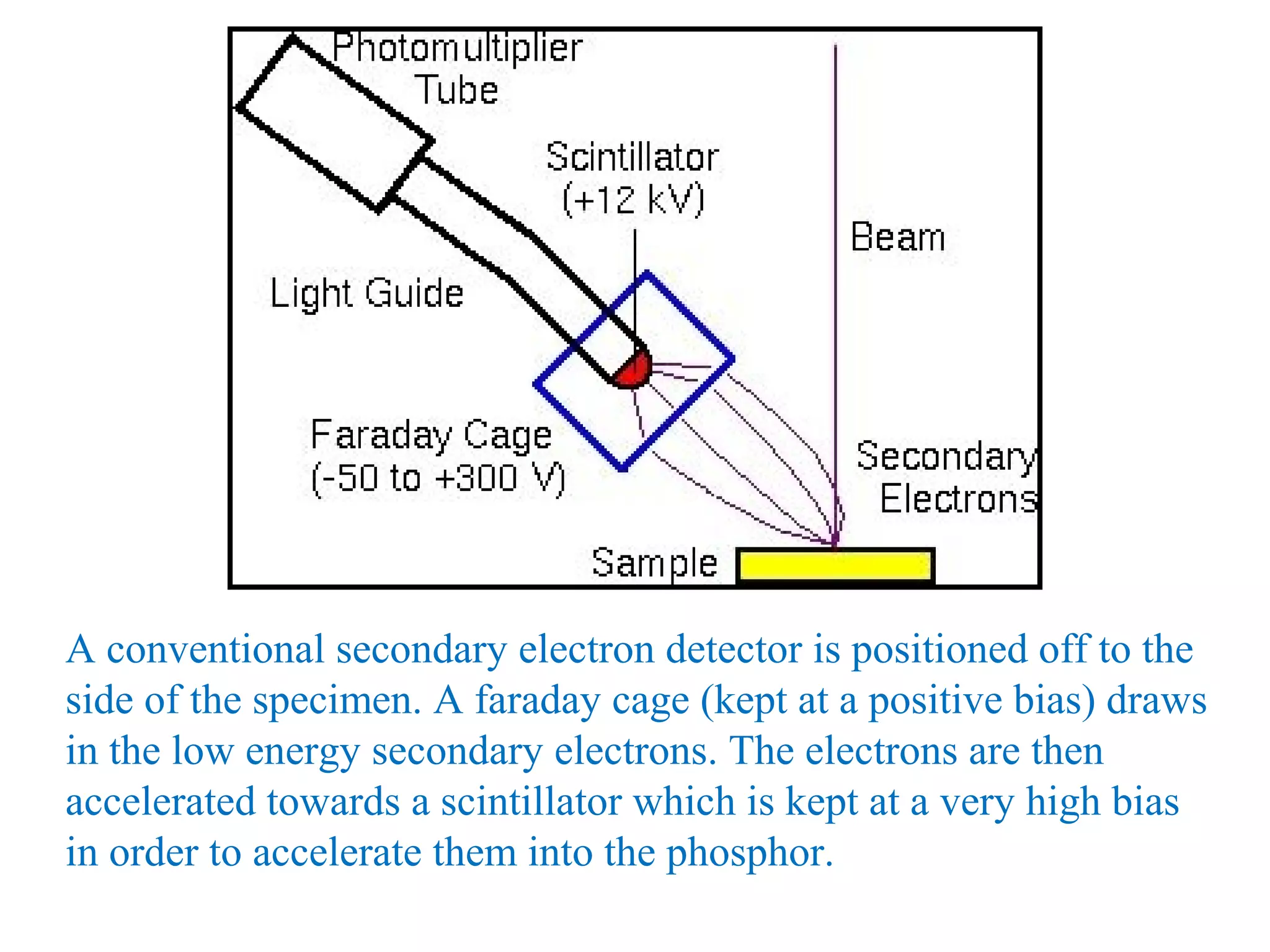
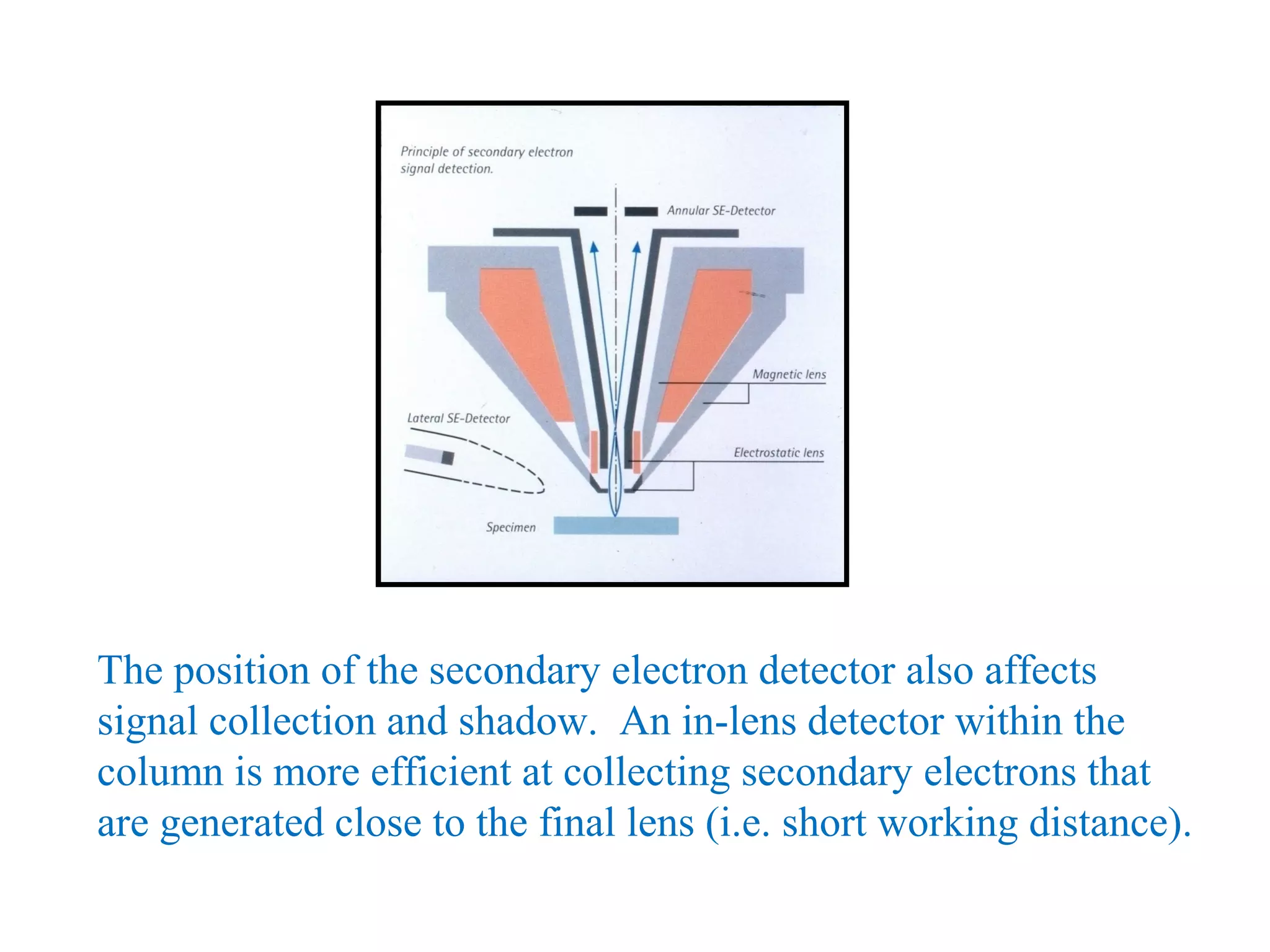
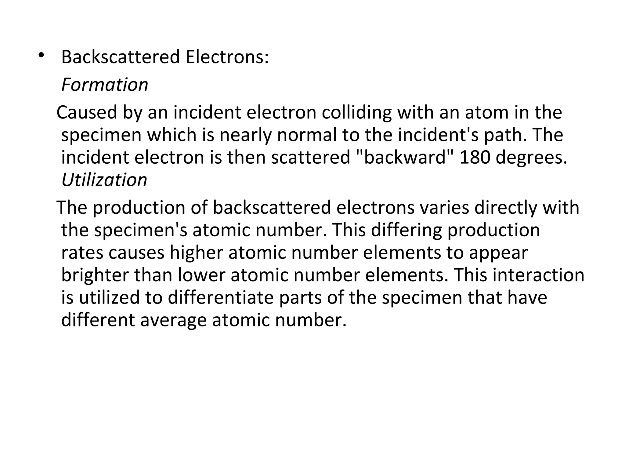
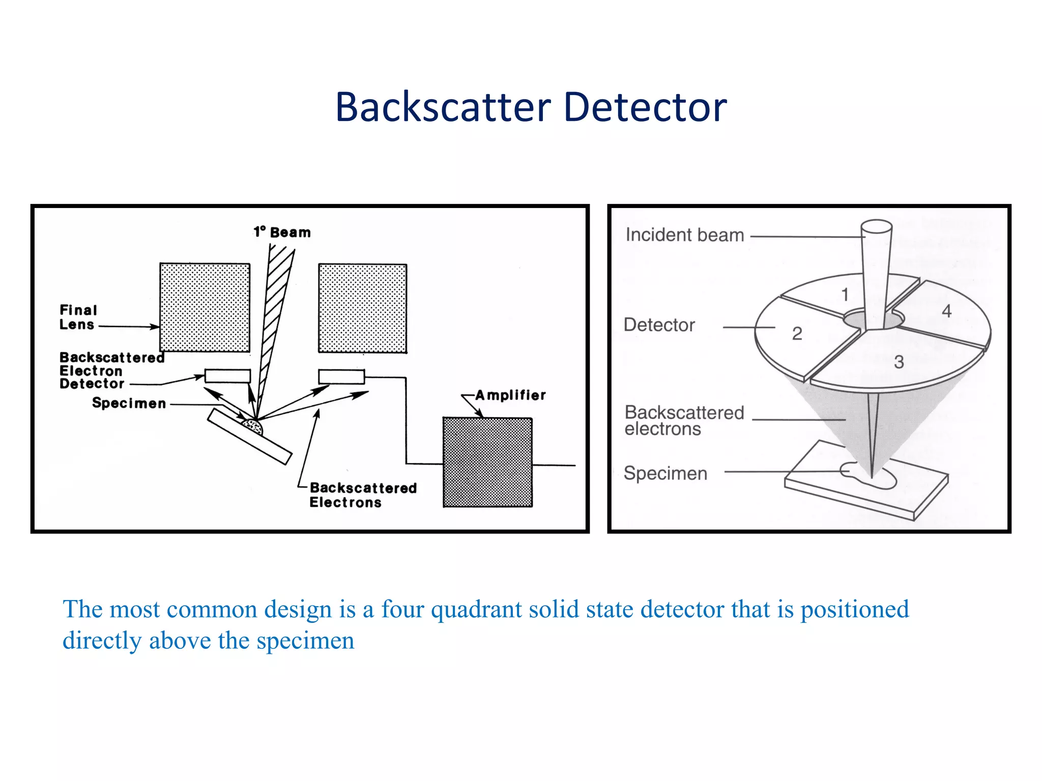
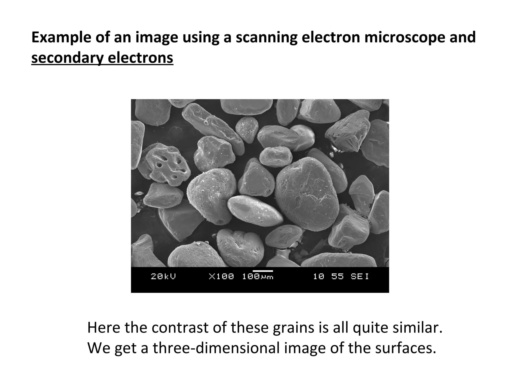
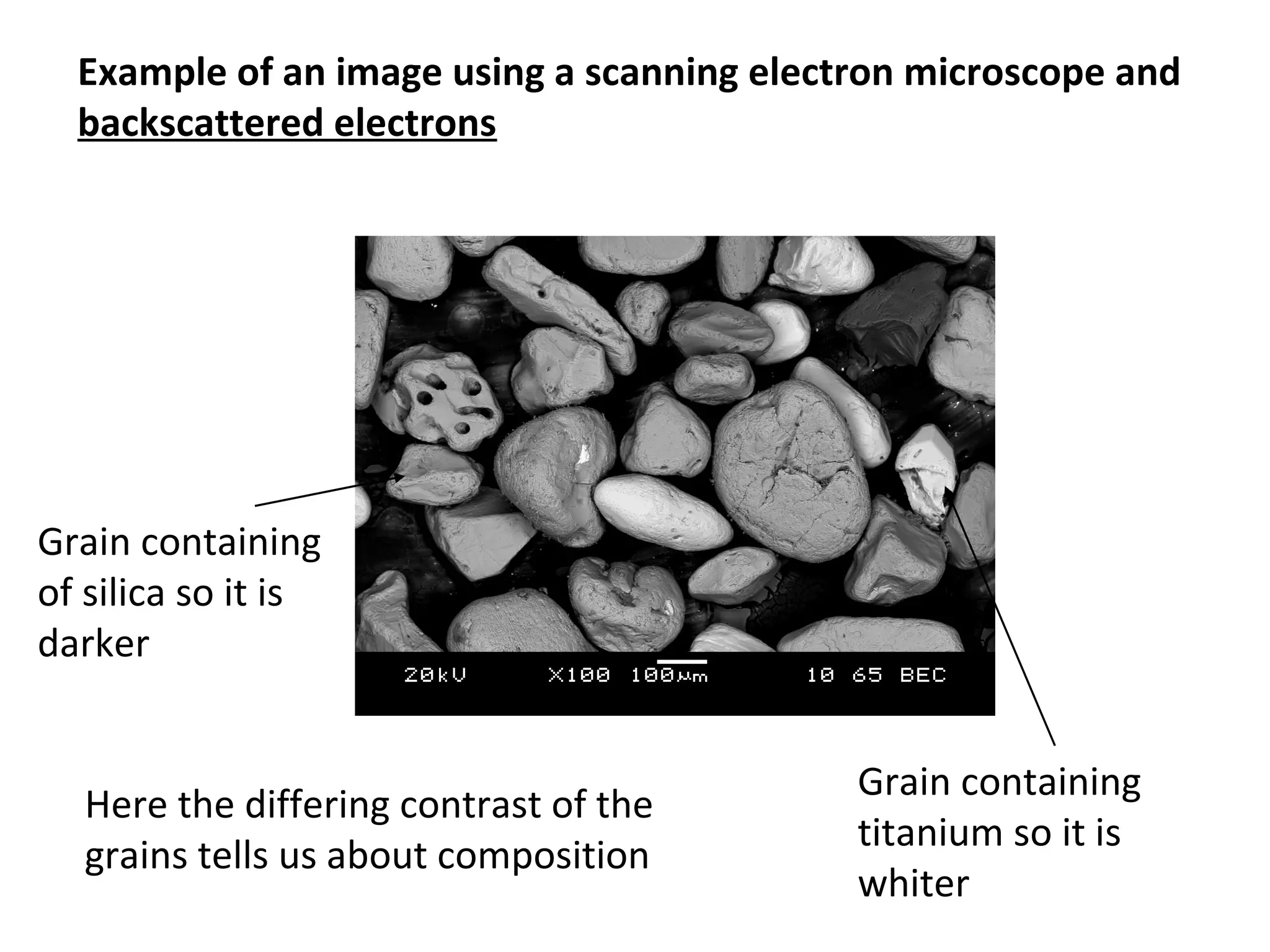
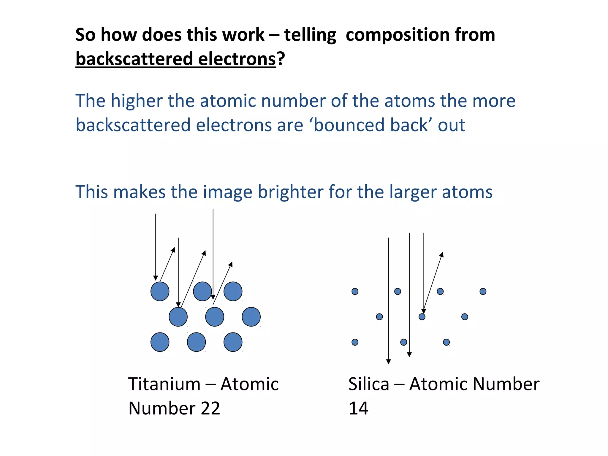
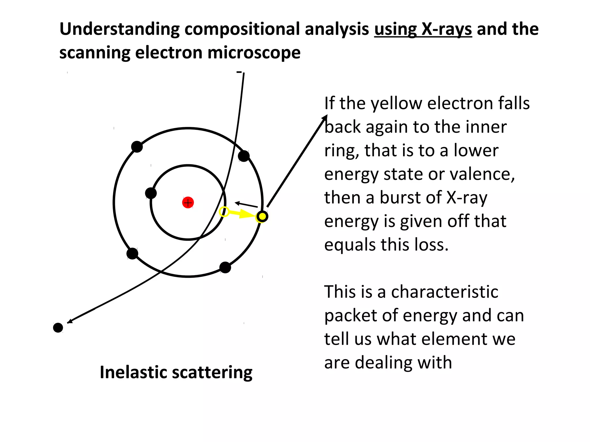
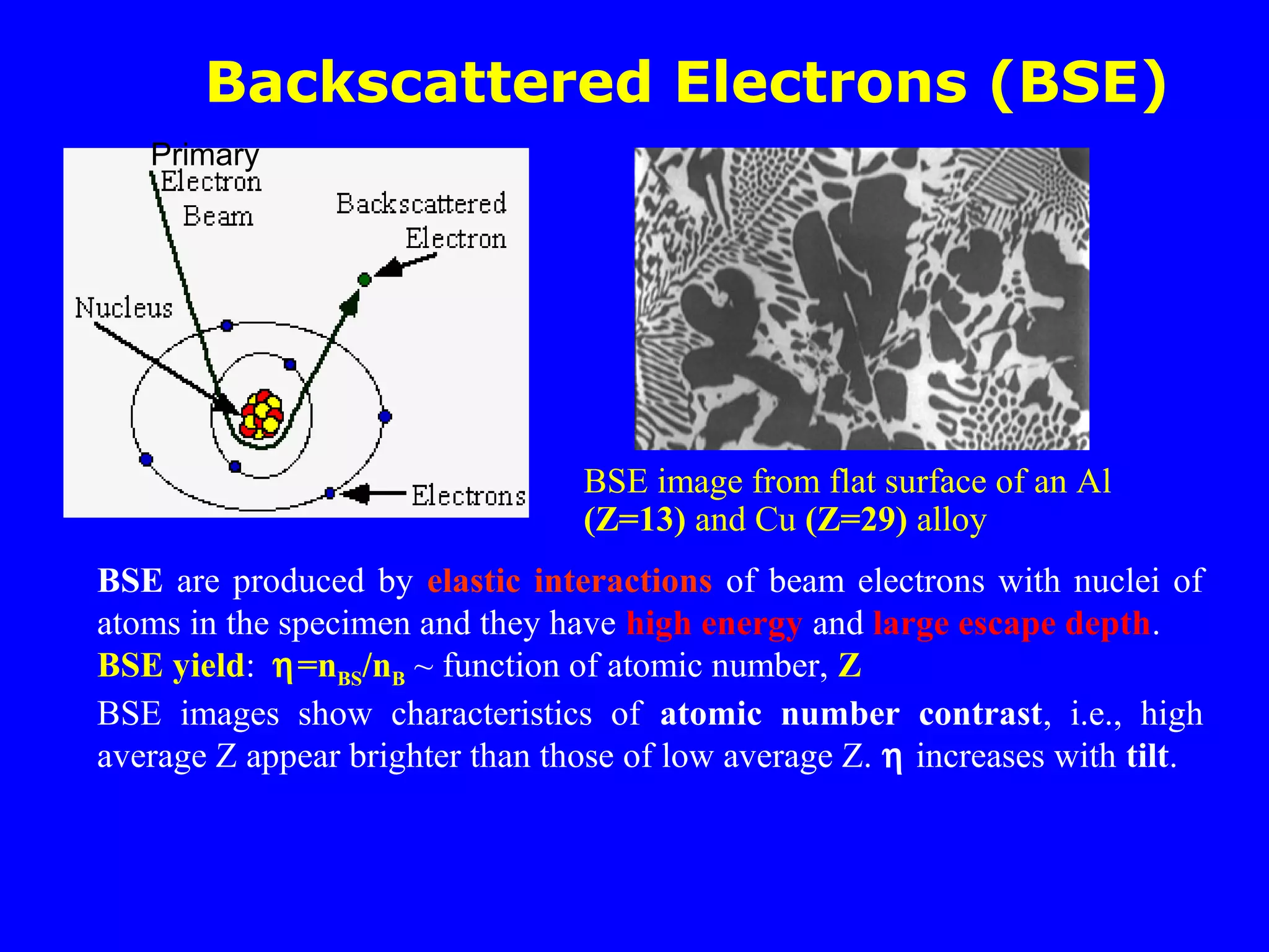
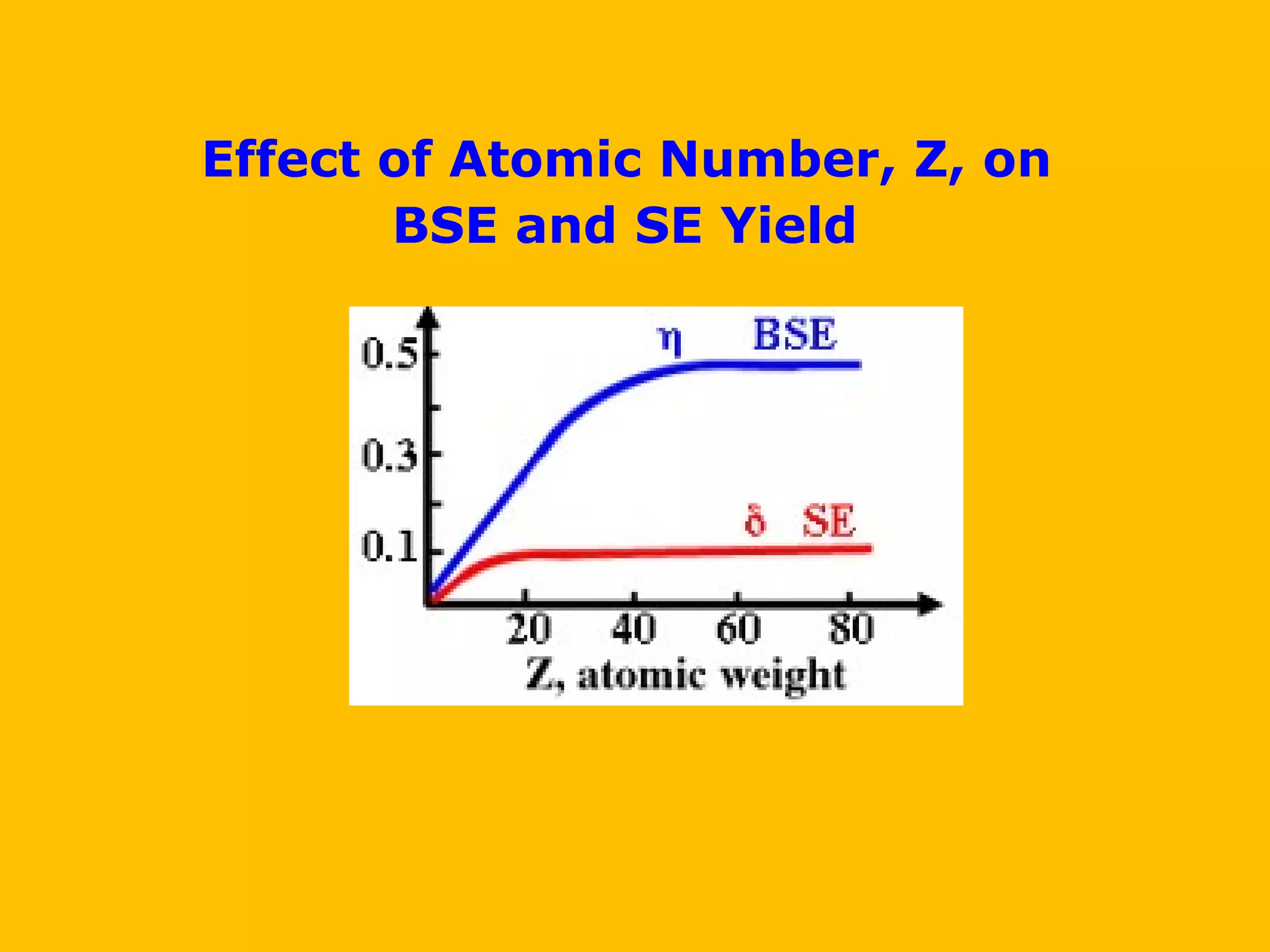
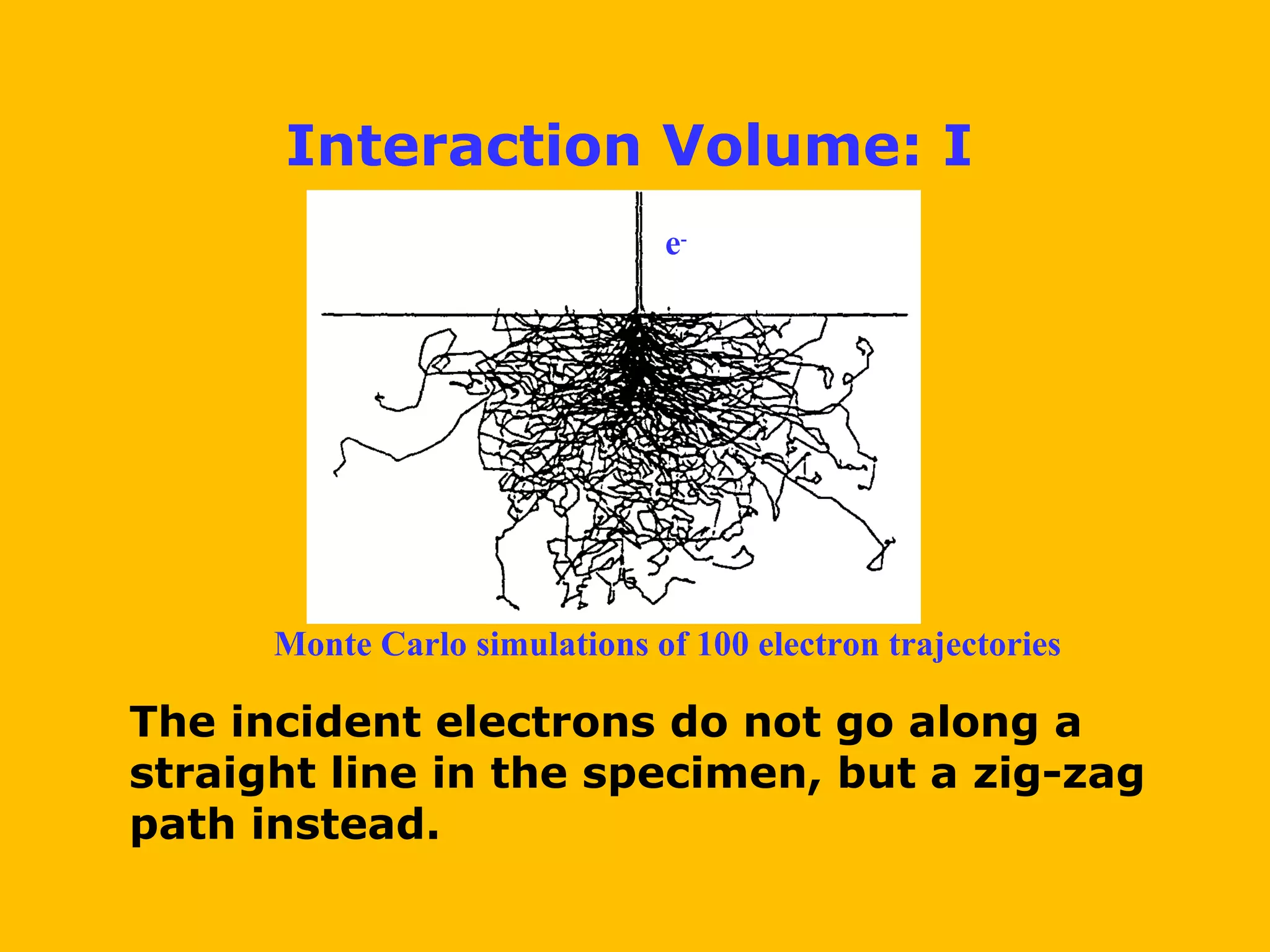
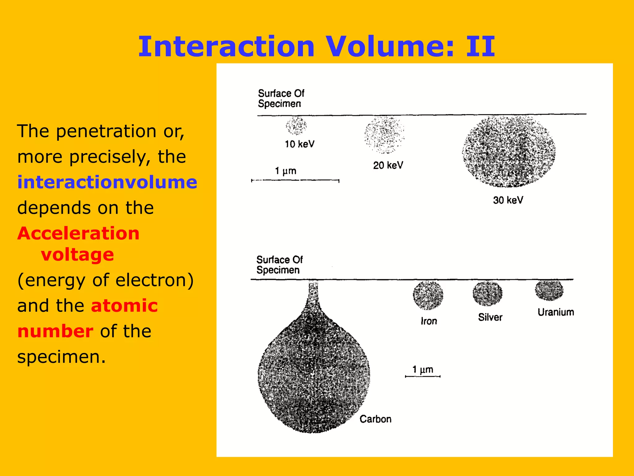
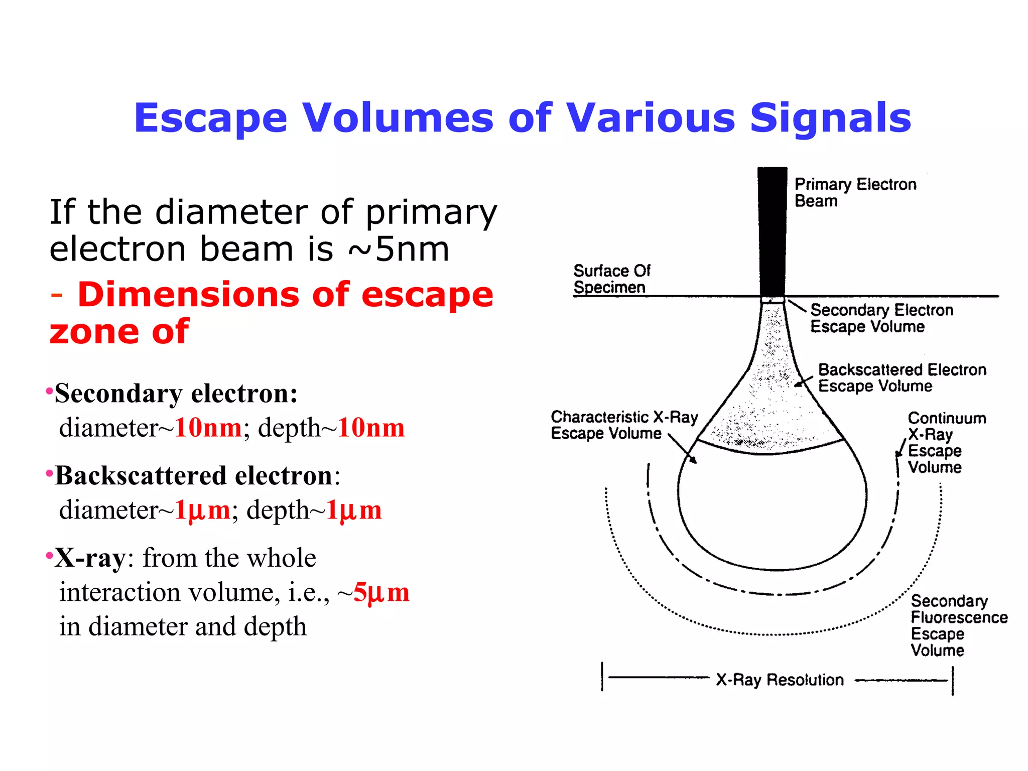
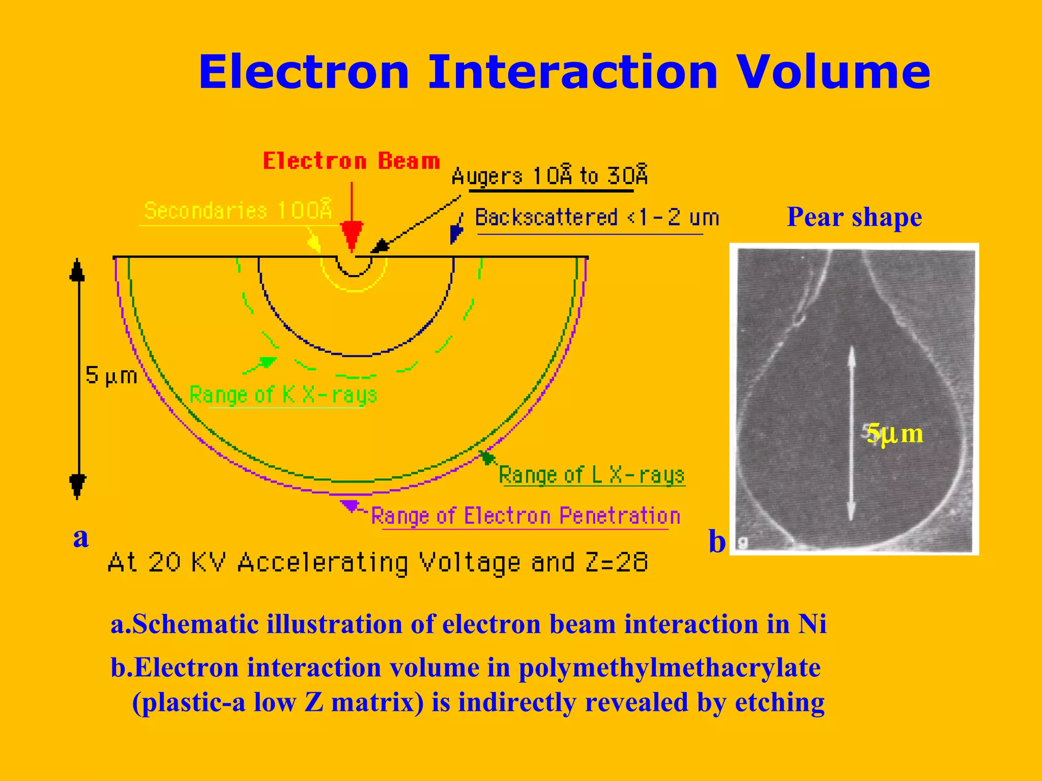
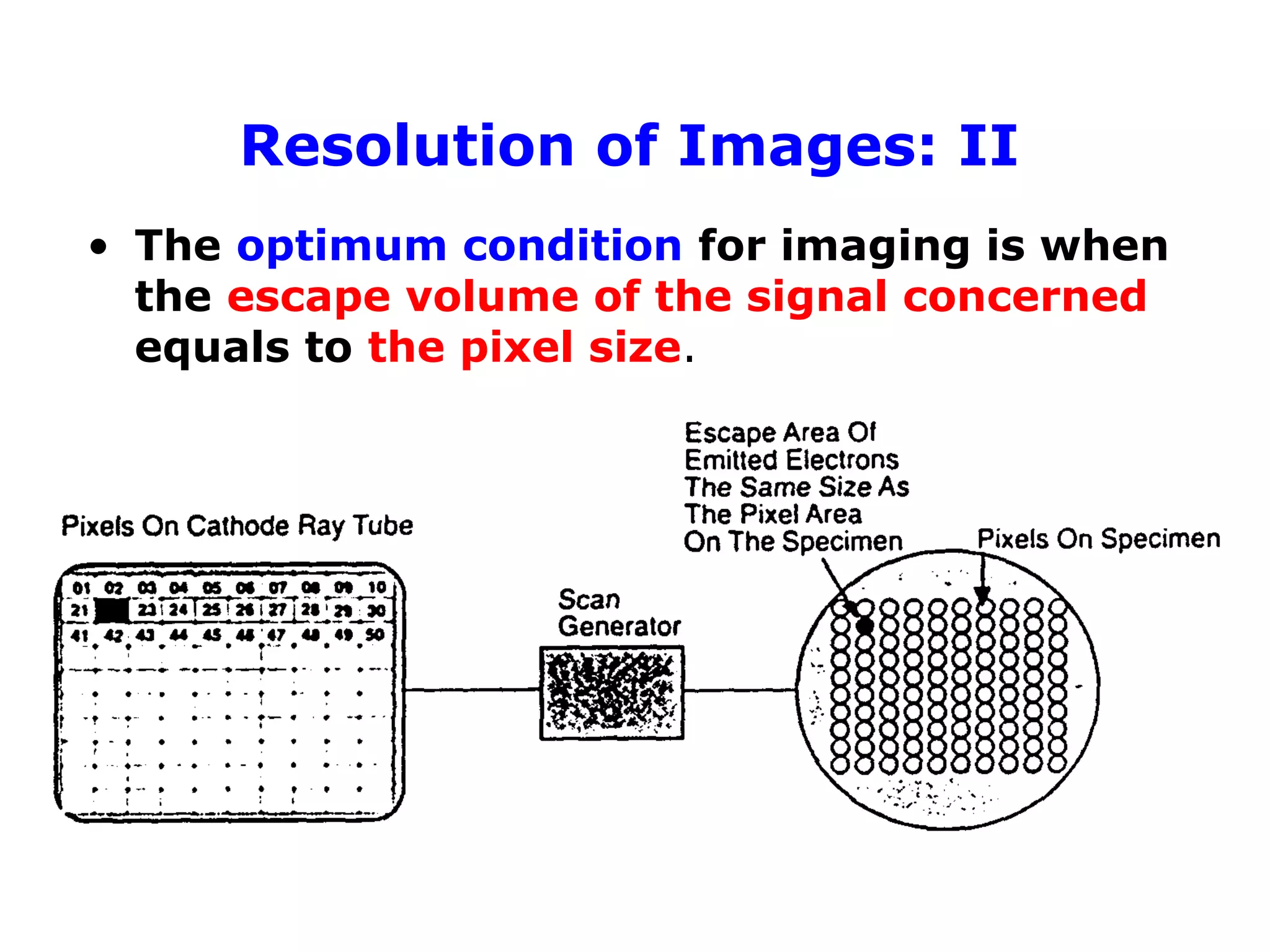
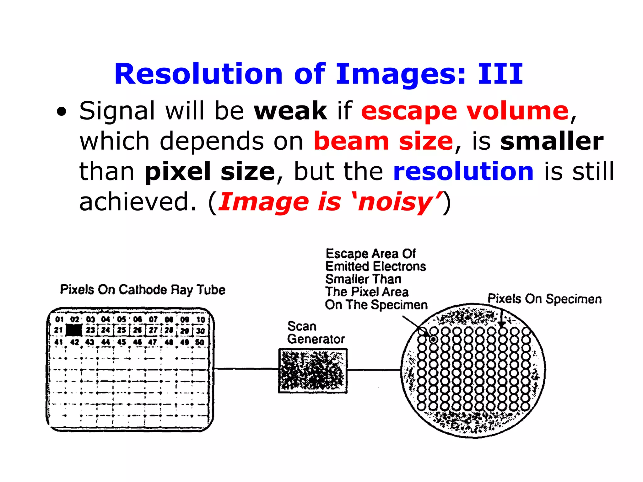
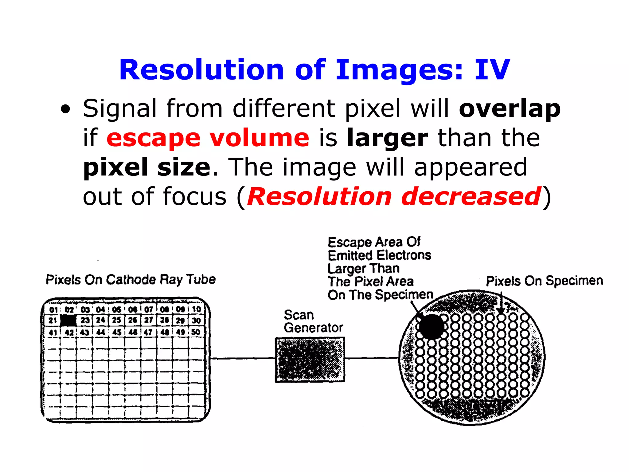
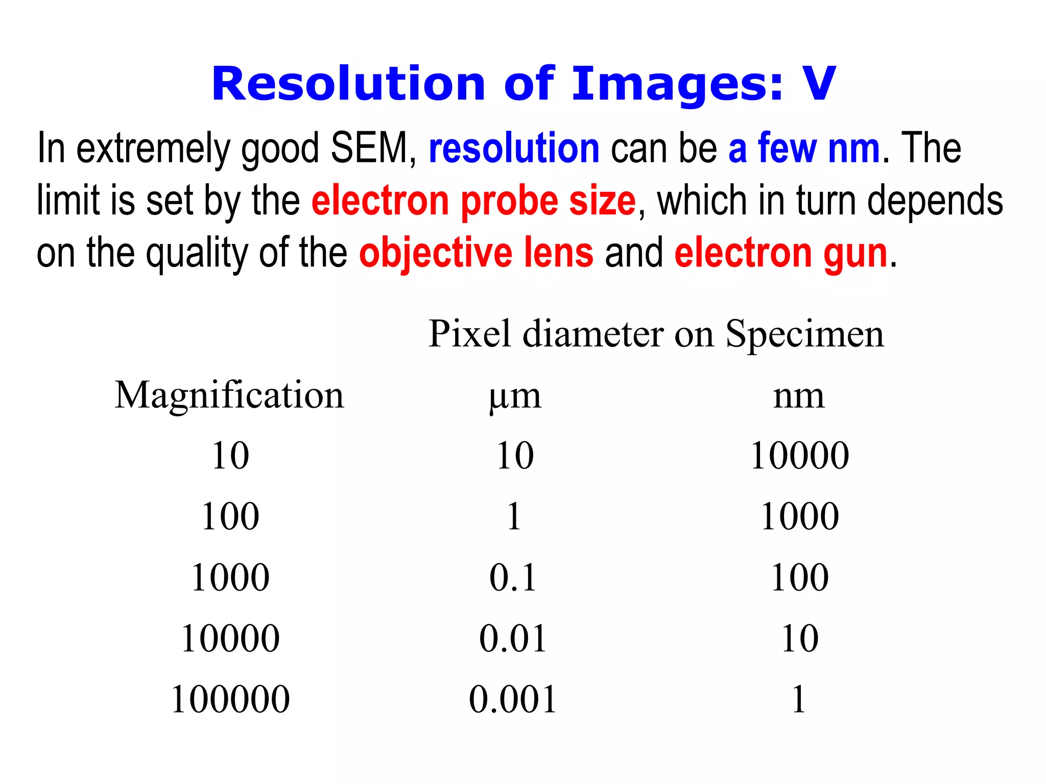
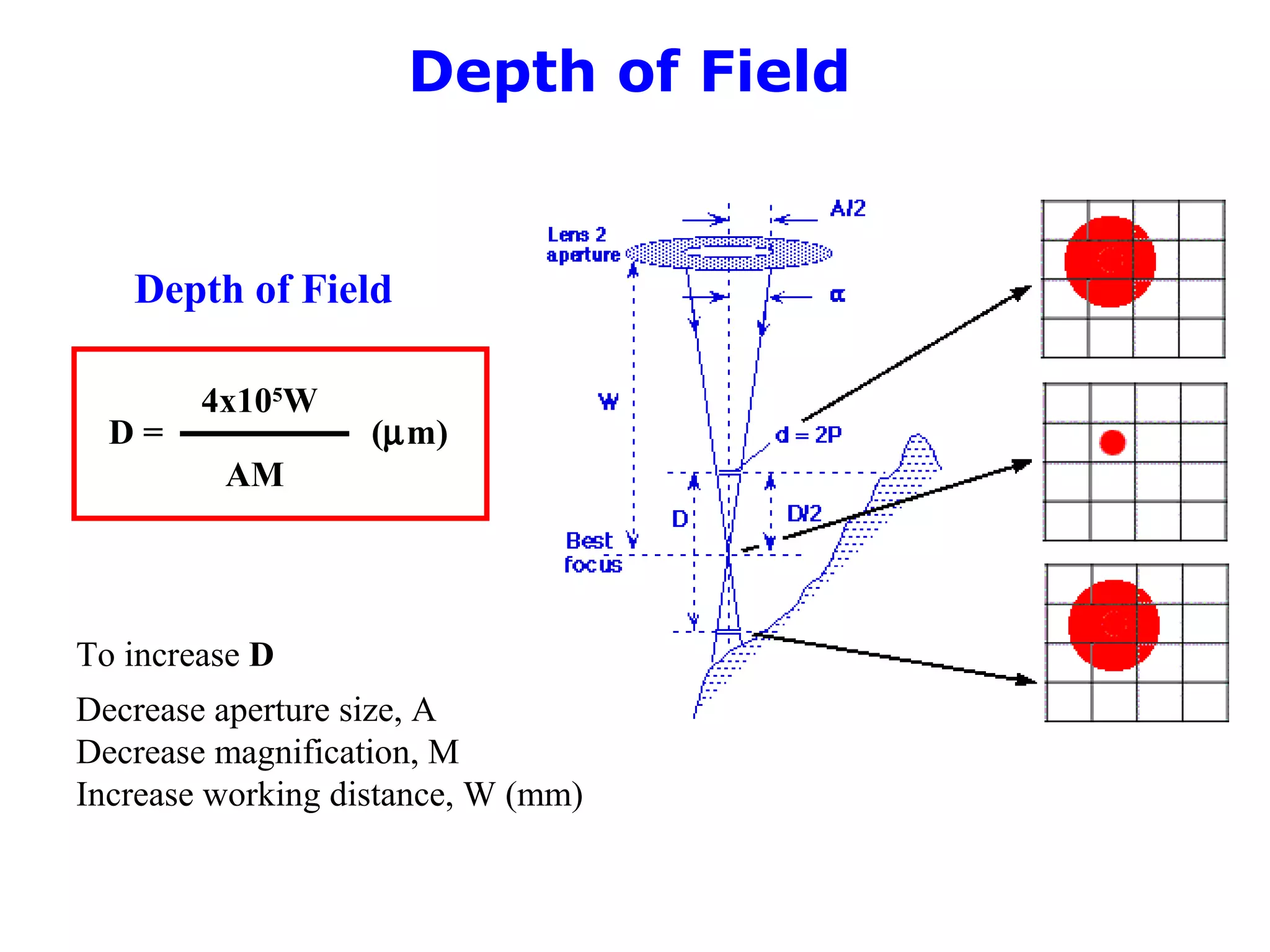
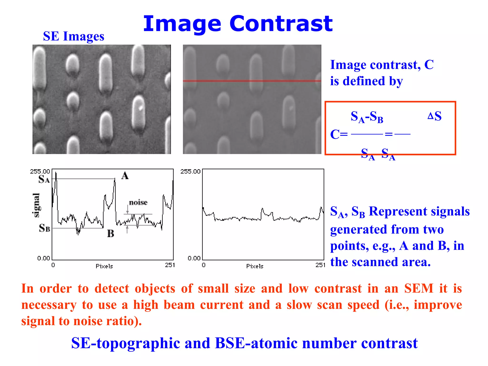
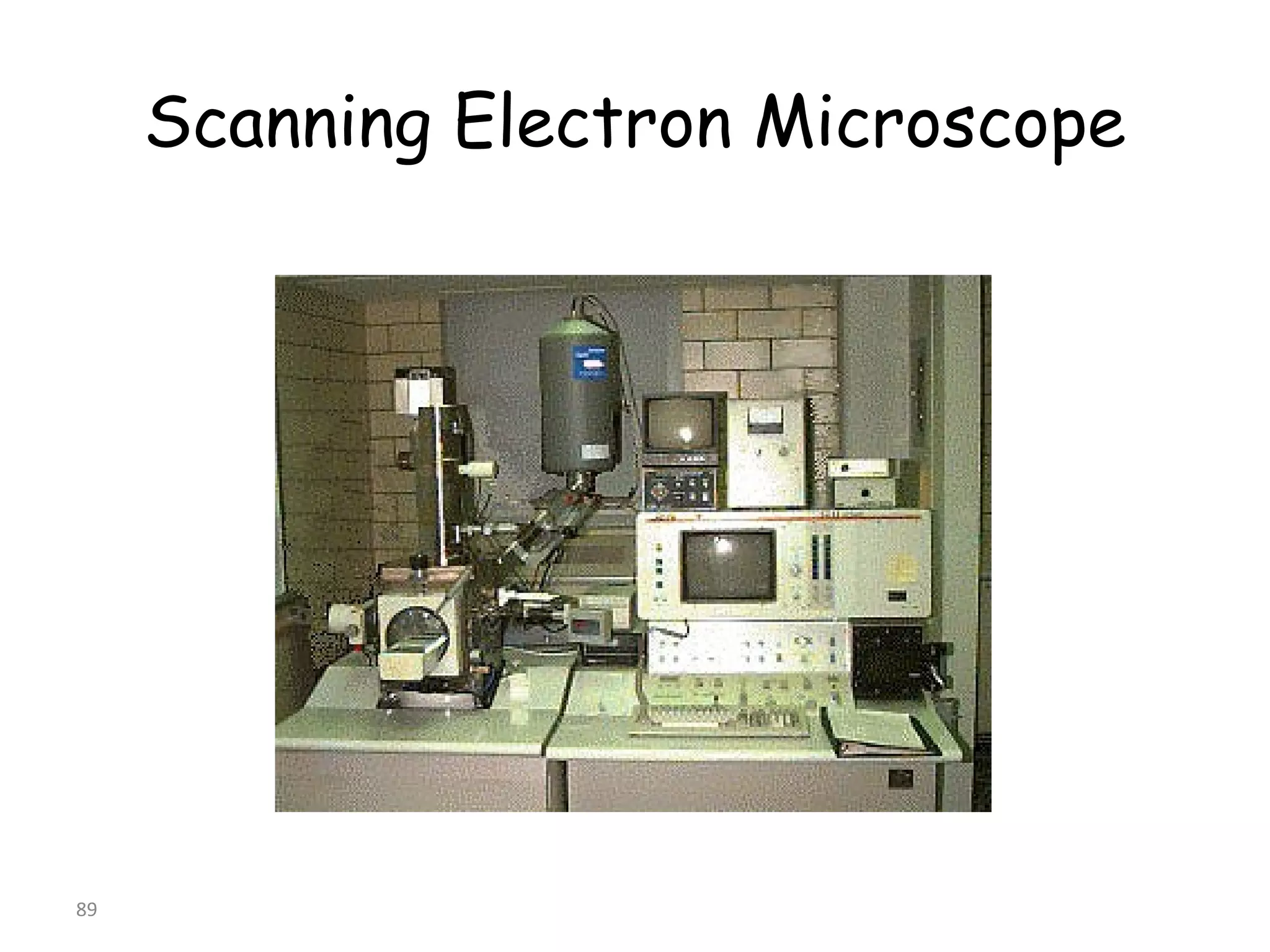
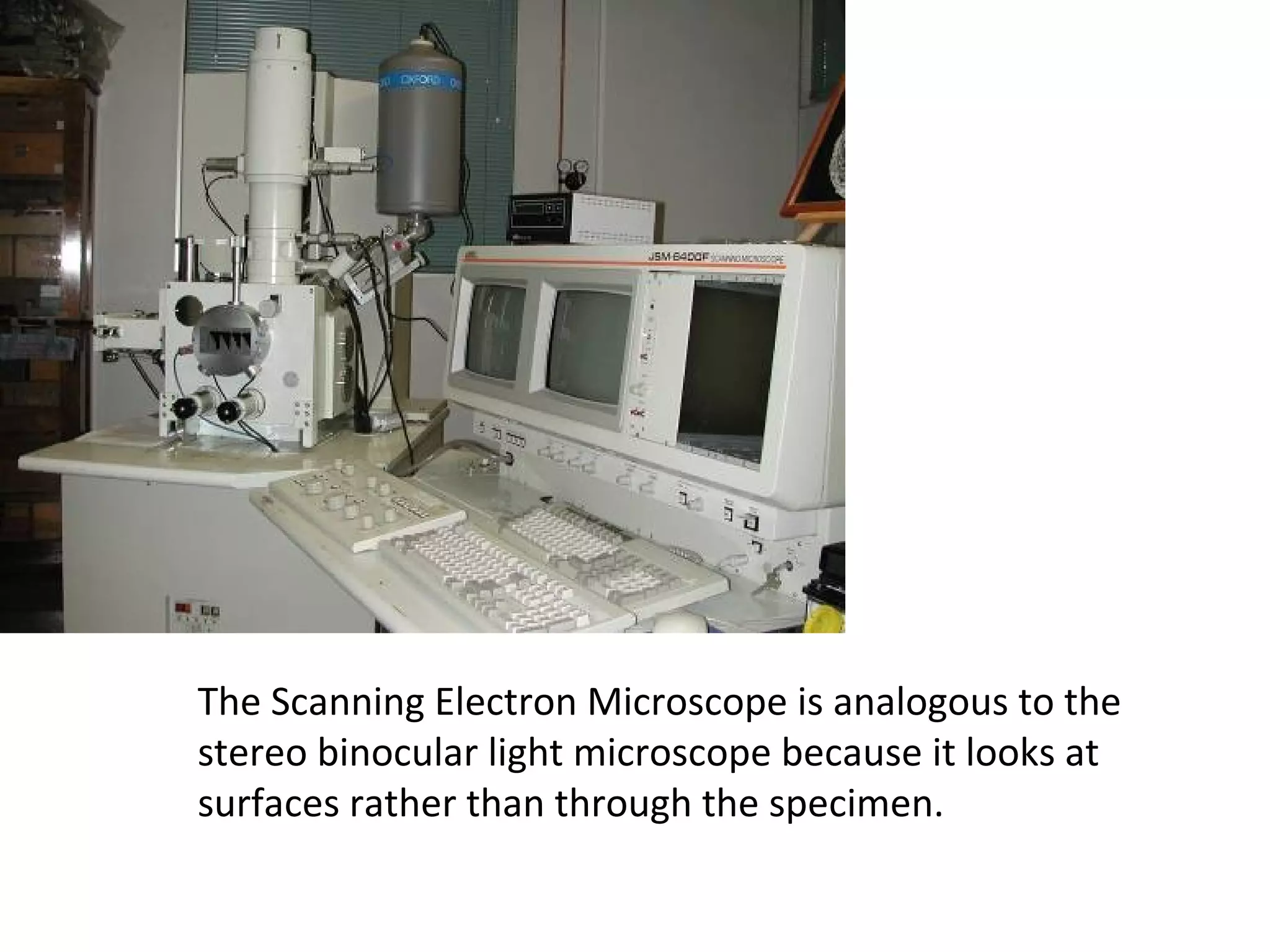
ELECTRON MICROSCOPY
DR. HARSH MOHAN
DEPARTMENT OF PHYSICS
M.L.N. COLLEGE
YAMUNA NAGAR
(HARYANA)
Scanning Electron Microscopy (SEM)
Scanning electron Microscope
(SEM):Principle, Instrumentation,
Electron optics, Magnification,
Application,
• type of electron microscope capable of producing high-
resolution images of a sample surface.
• due to the manner in which the image is created, SEM
images have a characteristic 3D appearance and are
useful for judging the surface structure of the sample.
Resolution
• depends on the size of the electron spot, which in turn
depends on the magnetic electron-optical system which
produces the scanning beam.
• is not high enough to image individual atoms, as is
possible in the TEM … so that, it is 1-20 nm
Scanning Electron Microscopy (SEM)
Scanning Electron Microscope
– a Totally Different Imaging Concept
• Instead of using the full-field image, a point-to-
point measurement strategy is used.
• High energy electron beam is used to excite the
specimen and the signals are collected and analyzed
so that an image can be constructed.
• The signals carry topological, chemical and
crystallographic information, respectively, of the
samples surface.
Advantages of Using SEM over OM
Magnification Depth of Field Resolution
OM 4x – 1000x 15.5mm – 0.19mm ~ 0.2mm
SEM 10x – 3000000x 4mm – 0.4mm 1-10nm
The SEM has a large depth of field, which allows a large amount of the
sample to be in focus at one time and produces an image that is a good
representation of the three-dimensional sample. The SEM also produces
images of high resolution, which means that closely features can be
examined at a high magnification.
The combination of higher magnification, larger depth of field, greater
resolution and compositional and crystallographic information makes the
SEM one of the most heavily used instruments in research areas and
industries, especially in semiconductor industry.
Scanning electron microscopy is used for inspecting topographies of specimens at
very high magnifications using a piece of equipment called the scanning electron
microscope. SEM magnifications can go to more than 300,000 X but most
semiconductor manufacturing applications require magnifications of less than 3,000
X only. SEM inspection is often used in the analysis of die/package cracks and
fracture surfaces, bond failures, and physical defects on the die or package surface.
During SEM inspection, a beam of electrons is focused on a spot volume of the
specimen, resulting in the transfer of energy to the spot. These bombarding
electrons, also referred to as primary electrons, dislodge electrons from the
specimen itself. The dislodged electrons, also known as secondary electrons, are
attracted and collected by a positively biased grid or detector, and then translated
into a signal.
To produce the SEM image, the electron beam is swept across the area being
inspected, producing many such signals. These signals are then amplified, analyzed,
and translated into images of the topography being inspected. Finally, the image is
shown on a CRT.
Scanning Electron Microscopy (SEM)
Electron-specimen interaction
Electron Beam and Specimen Interactions
Electron/Specimen InteractionsSources of Image Information
(1-50KeV)
Electron Beam Induced Current (EBIC)
Scanning Electron Microscopy (SEM)
• The energy of the primary electrons determines the quantity of
secondary electrons collected during inspection. The emission of
secondary electrons from the specimen increases as the energy of
the primary electron beam increases, until a certain limit is reached.
Beyond this limit, the collected secondary electrons diminish as the
energy of the primary beam is increased, because the primary beam
is already activating electrons deep below the surface of the
specimen. Electrons coming from such depths usually recombine
before reaching the surface for emission.
•
• Aside from secondary electrons, the primary electron beam results
in the emission of backscattered (or reflected) electrons from the
specimen. Backscattered electrons possess more energy than
secondary electrons, and have a definite direction. As such, they
can not be collected by a secondary electron detector, unless the
detector is directly in their path of travel. All emissions above 50 eV
are considered to be backscattered electrons.
• Backscattered electron imaging is useful in distinguishing one
material from another, since the yield of the collected backscattered
electrons increases monotonically with the specimen's atomic
number. Backscatter imaging can distinguish elements with atomic
number differences of at least 3, i.e., materials with atomic number
differences of at least 3 would appear with good contrast on the
image. For example, inspecting the remaining Au on an Al bond pad
after its Au ball bond has lifted off would be easier using backscatter
imaging, since the Au islets would stand out from the Al background.
•
• A SEM may be equipped with an EDX analysis system to enable it
to perform compositional analysis on specimens. EDX analysis is
useful in identifying materials and contaminants, as well as
estimating their relative concentrations on the surface of the
specimen.
Scanning Electron Microscopy (SEM)
Principles of SEM
Magnification?
Resolution?
Image Formation in SEM
beam
e-
Beam is scanned over specimen in a raster pattern in synchronization with
beam in CRT.
Intensity at A on CRT is proportional to signal detected from A on specimen
and signal is modulated by amplifier.
A
A
Detector
Amplifier
10cm
10cm
M= C/x
19
The Scanning Electron Microscope
• (SEM) bombards a specimen with a beam of
electrons instead of light
• Produces a highly magnified image from 100x to
100,0000
• Depth of focus 300X better than optical systems at
similar magnification
• Bombardment of the specimen’s surface with
electrons
– Produces x-ray emissions
– Characterize elements present in the material under
investigation
• An electron gun produces a beam of electrons that
scans the surface of a whole specimen.
• Secondary electrons emitted from the specimen
produce the image.
Scanning Electron Microscopy (SEM)
Figure 3.9b
Beam passes down the
microscope column
Electron beam now tends to
diverge
But is converged by
electromagnetic lenses
Cross section of
electromagnetic
lenses
Electron beam
produced here
Sample
Diagram of Scanning Electron Microscope or SEM
in cross section - the electrons are in green
23
Scanning Electron Microscope
SEM components
What is SEM
Scanning electron microscope (SEM) is a microscope that uses electrons
rather than light to form an image. There are many advantages to using the
SEM instead of a OM.
The SEM is designed
for direct studying of
the surfaces of solid
objects
Cost: $0.8-2.4M
Column
Sample
Chamber
TV Screens
A Look Inside the Column
Column
A more
detailed
look
inside
Source: L. Reimer,
“Scanning Electron
Microscope”, 2nd
Ed.,
Springer-Verlag, 1998, p.2
Electron Gun
e-
beam
α
Cathode Ray Tube (CRT) accelerates electrons towards the
phosphor coated screen where they produce flashes of light
upon hitting the phosphor. Deflection coilsDeflection coils create a scan
pattern forming an image in a point by point manner
Color CRT?
Image Magnification
Example of a series of increasing magnification (spherical lead particles imaged
in SE mode)
How an Electron Beam is Produced?
• Electron guns are used to produce a
fine, controlled beam of electrons
which are then focused at the
specimen surface.
• The electron guns may either be
thermionic gun or field-emission gun
Electron beam Source
W or LaB6 Filament
Thermionic or Field Emission Gun
Thermionic Emission Gun
• A tungsten filament
heated by DC to
approximately 2700K or
LaB6 rod heated to around
2000K
• A vacuum of 10-3
Pa (10-4
Pa for LaB6) is needed to
prevent oxidation of the
filament
• Electrons “boil off” from
the tip of the filament
• Electrons are accelerated
by an acceleration voltage
of 1-50kV
-
+
Source of Electrons
T: ~1500o
C
Thermionic Gun
W and LaB6 Cold- and thermal FEG
Electron Gun Properties
Source Brightness Stability(%) Size Energy spread Vacuum
W 3X10⁵
~1 50µm 3.0(eV) 10-5
(τ )
LaB6 3x10⁶
~2 5µm 1.5 10-6
C-FEG 109
~5 5nm 0.3 10-10
T-FEG 109
<1 20nm 0.7 10-9
(5-50µm)
E: >10MV/cm
(5nm)
Filament
W
Brightness – beam current density per unit solid angle
Electron Gun
W hairpin
LaB6 crystal
FEG
Thermionic Sources
Increasing the filament current will increase the beam current but
only to the point of saturation at which point an increase in the
filament current will only shorten the life of the emitter
Beam spot image at different stage of heating
Magnetic Lenses
• Condenser lens – focusing
determines the beam current
which impinges on the sample.
• Objective lens – final probe
forming
determines the final spot size of
the electron beam, i.e., the
resolution of a SEM.
Electromagnetic Lenses
An electromagnetic lens is essentially soft iron core wrapped in
wire
As we increase the current in the wire we increase the strength
of the magnetic field
Recall the right hand rule electron will move in a helical path
spiralling towards the centre of the magnetic field
Electromagnetic lens
Why Need a Vacuum?
When a SEM is used, the electron-optical column and
sample chamber must always be at a vacuum.
1. If the column is in a gas filled environment, electrons will be
scattered by gas molecules which would lead to reduction of the
beam intensity and stability.
2. Other gas molecules, which could come from the sample or the
microscope itself, could form compounds and condense on the
sample. This would lower the contrast and obscure detail in the
image.
The Condenser Lens
• For a thermionic gun, the diameter of
the first cross-over point ~20-50µm
• If we want to focus the beam to a size
< 10 nm on the specimen surface, the
magnification should be ~1/5000, which
is not easily attained with one lens (say,
the objective lens) only.
• Therefore, condenser lenses are added
to demagnify the cross-over points.
The objective lens
The objective lens aperture
Aperture in SEM: either to limit the amount of electrons or enhance contrast
How Is Electron Beam Focused?
A magnetic lens is a solenoid designed to produce
a specific magnetic flux distribution.
p
q
Magnetic lens
(solenoid)
Lens formula: 1/f = 1/p + 1/q
M = q/pDemagnification:
(Beam diameter)
F = -e(v x B)
f ∝ Bo
2
f can be adjusted by changing Bo, i.e., changing the current through
coil.
The Condenser
Lens
Demagnification:
M = f/L
C1 controls the spot size
C2 changes the convergence of the beam
Condenser-lens system
The condenser aperture must be centered
The Objective Lens
• The objective lens
controls the final
focus of the electron
beam by changing the
magnetic field strength
• The cross-over image is
finally demagnified to
an ~10nm beam spot
which carries a beam
current of
approximately 10-9
-10-
10-12
A.
The Objective Lens - Focusing
• By changing the
current in the
objective lens, the
magnetic field
strength changes
and therefore the
focal length of
the objective lens
is changed.
Out of focus in focus out of focus
lens current lens current lens current
too strong optimized too weak
Objective
lens
Depth of Field
Detector and sample stage
Electron Detectors and Sample Stage
Objective
lens
Sample stage
Topographical Contrast
Topographic contrast arises because SE generation depend on the
angle of incidence between the beam and sample.
Bright
Dark
+200V
e-
lens polepiece
SE
sample
Everhart-Thornley
SE Detector
Scintillator
light pipe
Quartz
window
+10kV
Faraday
cage
Photomultiplier
tube
PMT
Electron beam – Specimen Interaction. Note the two types
of electrons produced.
Electrons from the focused beam interact with the sample
to produce a spray of electrons up from the sample. These
come in two types – either secondary electrons or
backscattered electrons.
As the beam travels across (scans across) the sample the
spray of electrons is then collected little by little and forms
the image of our sample on a computer screen.
We can look more closely at these two types of electrons
because we use them for different purposes.
+
-
Inelastic scattering
+
-
Elastic scattering
Energy of electron from beam is
lost to atom
An incoming electron rebounds
back out (as a backscattered
electron)
A new electron is knocked
out (as a secondary
electron)
• Secondary Electrons:
Source
Caused by an incident electron passing "near" an atom in the specimen, near
enough to impart some of its energy to a lower energy electron (usually in the K-
shell). This causes a slight energy loss and path change in the incident electron and
the ionization of the electron in the specimen atom. This ionized electron then
leaves the atom with a very small kinetic energy (5eV) and is then termed a
"secondary electron". Each incident electron can produce several secondary
electrons.
Utilization
Production of secondary electrons is very topography related. Due to their low
energy, 5eV, only secondaries that are very near the surface (< 10 nm) can exit the
sample and be examined. Any changes in topography in the sample that are larger
than this sampling depth will change the yield of secondaries due to collection
efficiencies. Collection of these electrons is aided by using a "collector" in
conjunction with the secondary electron detector. The collector is a grid or mesh
with a +100V potential applied to it which is placed in front of the detector,
attracting the negatively charged secondary electrons to it which then pass
through the grid-holes and into the detector to be counted.
A conventional secondary electron detector is positioned off to the
side of the specimen. A faraday cage (kept at a positive bias) draws
in the low energy secondary electrons. The electrons are then
accelerated towards a scintillator which is kept at a very high bias
in order to accelerate them into the phosphor.
The position of the secondary electron detector also affects
signal collection and shadow. An in-lens detector within the
column is more efficient at collecting secondary electrons that
are generated close to the final lens (i.e. short working distance).
Secondary Electron Detector
Side Mounted In-Lens
What are the differences between these two images?
• Backscattered Electrons:
Formation
Caused by an incident electron colliding with an atom in the
specimen which is nearly normal to the incident's path. The
incident electron is then scattered "backward" 180 degrees.
Utilization
The production of backscattered electrons varies directly with
the specimen's atomic number. This differing production
rates causes higher atomic number elements to appear
brighter than lower atomic number elements. This interaction
is utilized to differentiate parts of the specimen that have
different average atomic number.
The most common design is a four quadrant solid state detector that is positioned
directly above the specimen
Backscatter Detector
Example of an image using a scanning electron microscope and
secondary electrons
Here the contrast of these grains is all quite similar.
We get a three-dimensional image of the surfaces.
Grain containing
titanium so it is
whiter
Grain containing
of silica so it is
darker
Example of an image using a scanning electron microscope and
backscattered electrons
Here the differing contrast of the
grains tells us about composition
So how does this work – telling composition from
backscattered electrons?
The higher the atomic number of the atoms the more
backscattered electrons are ‘bounced back’ out
This makes the image brighter for the larger atoms
Titanium – Atomic
Number 22
Silica – Atomic Number
14
+
-
Inelastic scattering
If the yellow electron falls
back again to the inner
ring, that is to a lower
energy state or valence,
then a burst of X-ray
energy is given off that
equals this loss.
This is a characteristic
packet of energy and can
tell us what element we
are dealing with
Understanding compositional analysis using X-rays and the
scanning electron microscope
Backscattered Electrons (BSE)
BSE are produced by elastic interactions of beam electrons with nuclei of
atoms in the specimen and they have high energy and large escape depth.
BSE yield: η=nBS/nB ~ function of atomic number, Z
BSE images show characteristics of atomic number contrast, i.e., high
average Z appear brighter than those of low average Z. η increases with tilt.
Primary
BSE image from flat surface of an Al
(Z=13) and Cu (Z=29) alloy
Effect of Atomic Number, Z, on
BSE and SE Yield
Interaction Volume: I
The incident electrons do not go along a
straight line in the specimen, but a zig-zag
path instead.
Monte Carlo simulations of 100 electron trajectories
e-
Interaction Volume: II
The penetration or,
more precisely, the
interactionvolume
depends on the
Acceleration
voltage
(energy of electron)
and the atomic
number of the
specimen.
Escape Volume of Various SignalsEscape Volume of Various Signals
• The incident electrons interact with specimen
atoms along their path in the specimen and
generate various signals.
• Owing to the difference in energy of these
signals, their ‘penetration depths’ are
different
• Therefore different signal observable on the
specimen surface comes from different parts
of the interaction volume
• The volume responsible for the respective
signal is called the escape volume of that
signal.
If the diameter of primary
electron beam is ~5nm
- Dimensions of escape
zone of
Escape Volumes of Various Signals
•Secondary electron:
diameter~10nm; depth~10nm
•Backscattered electron:
diameter~1µm; depth~1µm
•X-ray: from the whole
interaction volume, i.e., ~5µm
in diameter and depth
Electron Interaction Volume
5µm
a b
a.Schematic illustration of electron beam interaction in Ni
b.Electron interaction volume in polymethylmethacrylate
(plastic-a low Z matrix) is indirectly revealed by etching
Pear shape
Magnification
The magnification is simply the ratio of the length of the scan C on the
Cathode Ray Tube (CRT) to the length of the scan x on the specimen. For a
CRT screen that is 10 cm square:
M= C/x = 10cm/x
Increasing M is achieved by decreasing x.
M x M x
100 1 mm 10000 10 µm
1000 100 µm 100000 1 µm
Low M
Large x
40µm
High M
small x
7µm
2500x 15000x
1.2µm
e-
x
Resolution Limitations
Ultimate resolution obtainable in an SEM image can be
limited by:
1. Electron Optical limitations
Diffraction: dd=1.22λ/α
for a 20-keV beam, λ =0.0087nm and α=5x10⁻³
dd=2.1nm
Chromatic and spherical aberrations: dmin=1.29λ3/4
Cs
1/4
A SEM fitted with an FEG has an achievable resolution of ~1.0nm at 30 kV
due to smaller Cs (~20mm) and λ.
2. Specimen Contrast Limitations
Contrast dmin
1.0 2.3nm
0.5 4.6nm
0.1 23nm
0.01 230nm
3. Sampling Volume Limitations (Escape volume)
How Fine Can We See with SEM?
• If we can scan an area with width 10 nm
(10,000,000×) we may actually see
atoms!! But, can we?
• Image on the CRT consists of spots called
pixels (e.g. your PC screen displays
1024×768 pixels of ~0.25mm pitch)
which are the basic units in the image.
• You cannot have details finer than
one pixel!
Resolution of Images: I
• Assume that there the screen can display 1000
pixels/(raster line), then you can imagine that
there are 1000 pixels on each raster line on the
specimen.
• The resolution is the pixel diameter on
specimen surface.
P=D/Mag = 100um/Mag
P-pixel diameter on specimen surface
D-pixel diameter on CRT, Mag-magnification
Mag P(µm) Mag P(nm)
10x 10 10kx 10
1kx 0.1 100kx 1
• The optimum condition for imaging is when
the escape volume of the signal concerned
equals to the pixel size.
Resolution of Images: II
• Signal will be weak if escape volume,
which depends on beam size, is smaller
than pixel size, but the resolution is still
achieved. (Image is ‘noisy’)
Resolution of Images: III
Resolution of Images: IV
• Signal from different pixel will overlap
if escape volume is larger than the
pixel size. The image will appeared
out of focus (Resolution decreased)
Resolution of Images: V
Pixel diameter on Specimen
Magnification µm nm
10 10 10000
100 1 1000
1000 0.1 100
10000 0.01 10
100000 0.001 1
In extremely good SEM, resolution can be a few nm. The
limit is set by the electron probe size, which in turn depends
on the quality of the objective lens and electron gun.
Depth of Field
D = (µm)
AM
4x10⁵
W
To increase D
Decrease aperture size, A
Decrease magnification, M
Increase working distance, W (mm)
Depth of Field
Image Contrast
Image contrast, C
is defined by
SA-SB ∆S
C= ________
=____
SA SA
SA, SB Represent signals
generated from two
points, e.g., A and B, in
the scanned area.
In order to detect objects of small size and low contrast in an SEM it is
necessary to use a high beam current and a slow scan speed (i.e., improve
signal to noise ratio).
SE-topographic and BSE-atomic number contrast
SE Images
89
Scanning Electron Microscope
The Scanning Electron Microscope is analogous to the
stereo binocular light microscope because it looks at
surfaces rather than through the specimen.
Main Applications
• Topography
The surface features of an object and its texture
(hardness, reflectivity… etc.)
• Morphology
The shape and size of the particles making up the
object (strength, defects in IC and chips...etc.)
• Composition
The elements and compounds that the object is
composed of and the relative amounts of them
(melting point, reactivity, hardness...etc.)
• Crystallographic Information
How the grains are arranged in the object
(conductivity, electrical properties, strength...etc.)
SE Images - Topographic Contrast
The debris shown here is an oxide fiber
got stuck at a semiconductor device
detected by SEM
1µm
Defect in a semiconductor device Molybdenum
trioxide crystals
BSE Image – Atomic Number Contrast
BSE atomic number contrast image showing a niobium-rich
intermetallic phase (bright contrast) dispersed in an alumina matrix
(dark contrast).
Z (Nb) = 41, Z (Al) = 13 and Z(O) = 8
Alumina-Al2O3
2µm
Can you see the
difference?
TEM SEMLIGH
T
We learn more from mistakes than successes…
2018 HM-scanning electron microscope

2018 HM-scanning electron microscope

  • 1.
    ELECTRON MICROSCOPY DR. HARSHMOHAN DEPARTMENT OF PHYSICS M.L.N. COLLEGE YAMUNA NAGAR (HARYANA)
  • 2.
  • 3.
    Scanning electron Microscope (SEM):Principle,Instrumentation, Electron optics, Magnification, Application,
  • 4.
    • type ofelectron microscope capable of producing high- resolution images of a sample surface. • due to the manner in which the image is created, SEM images have a characteristic 3D appearance and are useful for judging the surface structure of the sample. Resolution • depends on the size of the electron spot, which in turn depends on the magnetic electron-optical system which produces the scanning beam. • is not high enough to image individual atoms, as is possible in the TEM … so that, it is 1-20 nm Scanning Electron Microscopy (SEM)
  • 5.
    Scanning Electron Microscope –a Totally Different Imaging Concept • Instead of using the full-field image, a point-to- point measurement strategy is used. • High energy electron beam is used to excite the specimen and the signals are collected and analyzed so that an image can be constructed. • The signals carry topological, chemical and crystallographic information, respectively, of the samples surface.
  • 6.
    Advantages of UsingSEM over OM Magnification Depth of Field Resolution OM 4x – 1000x 15.5mm – 0.19mm ~ 0.2mm SEM 10x – 3000000x 4mm – 0.4mm 1-10nm The SEM has a large depth of field, which allows a large amount of the sample to be in focus at one time and produces an image that is a good representation of the three-dimensional sample. The SEM also produces images of high resolution, which means that closely features can be examined at a high magnification. The combination of higher magnification, larger depth of field, greater resolution and compositional and crystallographic information makes the SEM one of the most heavily used instruments in research areas and industries, especially in semiconductor industry.
  • 7.
    Scanning electron microscopyis used for inspecting topographies of specimens at very high magnifications using a piece of equipment called the scanning electron microscope. SEM magnifications can go to more than 300,000 X but most semiconductor manufacturing applications require magnifications of less than 3,000 X only. SEM inspection is often used in the analysis of die/package cracks and fracture surfaces, bond failures, and physical defects on the die or package surface. During SEM inspection, a beam of electrons is focused on a spot volume of the specimen, resulting in the transfer of energy to the spot. These bombarding electrons, also referred to as primary electrons, dislodge electrons from the specimen itself. The dislodged electrons, also known as secondary electrons, are attracted and collected by a positively biased grid or detector, and then translated into a signal. To produce the SEM image, the electron beam is swept across the area being inspected, producing many such signals. These signals are then amplified, analyzed, and translated into images of the topography being inspected. Finally, the image is shown on a CRT. Scanning Electron Microscopy (SEM)
  • 8.
  • 9.
    Electron Beam andSpecimen Interactions Electron/Specimen InteractionsSources of Image Information (1-50KeV) Electron Beam Induced Current (EBIC)
  • 13.
    Scanning Electron Microscopy(SEM) • The energy of the primary electrons determines the quantity of secondary electrons collected during inspection. The emission of secondary electrons from the specimen increases as the energy of the primary electron beam increases, until a certain limit is reached. Beyond this limit, the collected secondary electrons diminish as the energy of the primary beam is increased, because the primary beam is already activating electrons deep below the surface of the specimen. Electrons coming from such depths usually recombine before reaching the surface for emission. • • Aside from secondary electrons, the primary electron beam results in the emission of backscattered (or reflected) electrons from the specimen. Backscattered electrons possess more energy than secondary electrons, and have a definite direction. As such, they can not be collected by a secondary electron detector, unless the detector is directly in their path of travel. All emissions above 50 eV are considered to be backscattered electrons.
  • 14.
    • Backscattered electronimaging is useful in distinguishing one material from another, since the yield of the collected backscattered electrons increases monotonically with the specimen's atomic number. Backscatter imaging can distinguish elements with atomic number differences of at least 3, i.e., materials with atomic number differences of at least 3 would appear with good contrast on the image. For example, inspecting the remaining Au on an Al bond pad after its Au ball bond has lifted off would be easier using backscatter imaging, since the Au islets would stand out from the Al background. • • A SEM may be equipped with an EDX analysis system to enable it to perform compositional analysis on specimens. EDX analysis is useful in identifying materials and contaminants, as well as estimating their relative concentrations on the surface of the specimen. Scanning Electron Microscopy (SEM)
  • 17.
  • 18.
    Image Formation inSEM beam e- Beam is scanned over specimen in a raster pattern in synchronization with beam in CRT. Intensity at A on CRT is proportional to signal detected from A on specimen and signal is modulated by amplifier. A A Detector Amplifier 10cm 10cm M= C/x
  • 19.
    19 The Scanning ElectronMicroscope • (SEM) bombards a specimen with a beam of electrons instead of light • Produces a highly magnified image from 100x to 100,0000 • Depth of focus 300X better than optical systems at similar magnification • Bombardment of the specimen’s surface with electrons – Produces x-ray emissions – Characterize elements present in the material under investigation
  • 21.
    • An electrongun produces a beam of electrons that scans the surface of a whole specimen. • Secondary electrons emitted from the specimen produce the image. Scanning Electron Microscopy (SEM) Figure 3.9b
  • 22.
    Beam passes downthe microscope column Electron beam now tends to diverge But is converged by electromagnetic lenses Cross section of electromagnetic lenses Electron beam produced here Sample Diagram of Scanning Electron Microscope or SEM in cross section - the electrons are in green
  • 23.
  • 24.
  • 25.
    What is SEM Scanningelectron microscope (SEM) is a microscope that uses electrons rather than light to form an image. There are many advantages to using the SEM instead of a OM. The SEM is designed for direct studying of the surfaces of solid objects Cost: $0.8-2.4M Column Sample Chamber TV Screens
  • 26.
    A Look Insidethe Column Column
  • 31.
    A more detailed look inside Source: L.Reimer, “Scanning Electron Microscope”, 2nd Ed., Springer-Verlag, 1998, p.2 Electron Gun e- beam α
  • 32.
    Cathode Ray Tube(CRT) accelerates electrons towards the phosphor coated screen where they produce flashes of light upon hitting the phosphor. Deflection coilsDeflection coils create a scan pattern forming an image in a point by point manner
  • 33.
  • 34.
    Image Magnification Example ofa series of increasing magnification (spherical lead particles imaged in SE mode)
  • 35.
    How an ElectronBeam is Produced? • Electron guns are used to produce a fine, controlled beam of electrons which are then focused at the specimen surface. • The electron guns may either be thermionic gun or field-emission gun
  • 36.
    Electron beam Source Wor LaB6 Filament Thermionic or Field Emission Gun
  • 37.
    Thermionic Emission Gun •A tungsten filament heated by DC to approximately 2700K or LaB6 rod heated to around 2000K • A vacuum of 10-3 Pa (10-4 Pa for LaB6) is needed to prevent oxidation of the filament • Electrons “boil off” from the tip of the filament • Electrons are accelerated by an acceleration voltage of 1-50kV - +
  • 38.
    Source of Electrons T:~1500o C Thermionic Gun W and LaB6 Cold- and thermal FEG Electron Gun Properties Source Brightness Stability(%) Size Energy spread Vacuum W 3X10⁵ ~1 50µm 3.0(eV) 10-5 (τ ) LaB6 3x10⁶ ~2 5µm 1.5 10-6 C-FEG 109 ~5 5nm 0.3 10-10 T-FEG 109 <1 20nm 0.7 10-9 (5-50µm) E: >10MV/cm (5nm) Filament W Brightness – beam current density per unit solid angle
  • 39.
  • 40.
    Thermionic Sources Increasing thefilament current will increase the beam current but only to the point of saturation at which point an increase in the filament current will only shorten the life of the emitter
  • 41.
    Beam spot imageat different stage of heating
  • 43.
    Magnetic Lenses • Condenserlens – focusing determines the beam current which impinges on the sample. • Objective lens – final probe forming determines the final spot size of the electron beam, i.e., the resolution of a SEM.
  • 44.
    Electromagnetic Lenses An electromagneticlens is essentially soft iron core wrapped in wire As we increase the current in the wire we increase the strength of the magnetic field Recall the right hand rule electron will move in a helical path spiralling towards the centre of the magnetic field
  • 45.
  • 46.
    Why Need aVacuum? When a SEM is used, the electron-optical column and sample chamber must always be at a vacuum. 1. If the column is in a gas filled environment, electrons will be scattered by gas molecules which would lead to reduction of the beam intensity and stability. 2. Other gas molecules, which could come from the sample or the microscope itself, could form compounds and condense on the sample. This would lower the contrast and obscure detail in the image.
  • 47.
    The Condenser Lens •For a thermionic gun, the diameter of the first cross-over point ~20-50µm • If we want to focus the beam to a size < 10 nm on the specimen surface, the magnification should be ~1/5000, which is not easily attained with one lens (say, the objective lens) only. • Therefore, condenser lenses are added to demagnify the cross-over points.
  • 48.
  • 49.
    The objective lensaperture Aperture in SEM: either to limit the amount of electrons or enhance contrast
  • 50.
    How Is ElectronBeam Focused? A magnetic lens is a solenoid designed to produce a specific magnetic flux distribution. p q Magnetic lens (solenoid) Lens formula: 1/f = 1/p + 1/q M = q/pDemagnification: (Beam diameter) F = -e(v x B) f ∝ Bo 2 f can be adjusted by changing Bo, i.e., changing the current through coil.
  • 51.
  • 52.
    C1 controls thespot size C2 changes the convergence of the beam Condenser-lens system The condenser aperture must be centered
  • 53.
    The Objective Lens •The objective lens controls the final focus of the electron beam by changing the magnetic field strength • The cross-over image is finally demagnified to an ~10nm beam spot which carries a beam current of approximately 10-9 -10- 10-12 A.
  • 54.
    The Objective Lens- Focusing • By changing the current in the objective lens, the magnetic field strength changes and therefore the focal length of the objective lens is changed. Out of focus in focus out of focus lens current lens current lens current too strong optimized too weak Objective lens
  • 55.
  • 56.
  • 57.
    Electron Detectors andSample Stage Objective lens Sample stage
  • 58.
    Topographical Contrast Topographic contrastarises because SE generation depend on the angle of incidence between the beam and sample. Bright Dark +200V e- lens polepiece SE sample Everhart-Thornley SE Detector Scintillator light pipe Quartz window +10kV Faraday cage Photomultiplier tube PMT
  • 59.
    Electron beam –Specimen Interaction. Note the two types of electrons produced.
  • 60.
    Electrons from thefocused beam interact with the sample to produce a spray of electrons up from the sample. These come in two types – either secondary electrons or backscattered electrons. As the beam travels across (scans across) the sample the spray of electrons is then collected little by little and forms the image of our sample on a computer screen. We can look more closely at these two types of electrons because we use them for different purposes.
  • 61.
    + - Inelastic scattering + - Elastic scattering Energyof electron from beam is lost to atom An incoming electron rebounds back out (as a backscattered electron) A new electron is knocked out (as a secondary electron)
  • 62.
    • Secondary Electrons: Source Causedby an incident electron passing "near" an atom in the specimen, near enough to impart some of its energy to a lower energy electron (usually in the K- shell). This causes a slight energy loss and path change in the incident electron and the ionization of the electron in the specimen atom. This ionized electron then leaves the atom with a very small kinetic energy (5eV) and is then termed a "secondary electron". Each incident electron can produce several secondary electrons. Utilization Production of secondary electrons is very topography related. Due to their low energy, 5eV, only secondaries that are very near the surface (< 10 nm) can exit the sample and be examined. Any changes in topography in the sample that are larger than this sampling depth will change the yield of secondaries due to collection efficiencies. Collection of these electrons is aided by using a "collector" in conjunction with the secondary electron detector. The collector is a grid or mesh with a +100V potential applied to it which is placed in front of the detector, attracting the negatively charged secondary electrons to it which then pass through the grid-holes and into the detector to be counted.
  • 63.
    A conventional secondaryelectron detector is positioned off to the side of the specimen. A faraday cage (kept at a positive bias) draws in the low energy secondary electrons. The electrons are then accelerated towards a scintillator which is kept at a very high bias in order to accelerate them into the phosphor.
  • 64.
    The position ofthe secondary electron detector also affects signal collection and shadow. An in-lens detector within the column is more efficient at collecting secondary electrons that are generated close to the final lens (i.e. short working distance).
  • 65.
    Secondary Electron Detector SideMounted In-Lens What are the differences between these two images?
  • 66.
    • Backscattered Electrons: Formation Causedby an incident electron colliding with an atom in the specimen which is nearly normal to the incident's path. The incident electron is then scattered "backward" 180 degrees. Utilization The production of backscattered electrons varies directly with the specimen's atomic number. This differing production rates causes higher atomic number elements to appear brighter than lower atomic number elements. This interaction is utilized to differentiate parts of the specimen that have different average atomic number.
  • 67.
    The most commondesign is a four quadrant solid state detector that is positioned directly above the specimen Backscatter Detector
  • 68.
    Example of animage using a scanning electron microscope and secondary electrons Here the contrast of these grains is all quite similar. We get a three-dimensional image of the surfaces.
  • 69.
    Grain containing titanium soit is whiter Grain containing of silica so it is darker Example of an image using a scanning electron microscope and backscattered electrons Here the differing contrast of the grains tells us about composition
  • 70.
    So how doesthis work – telling composition from backscattered electrons? The higher the atomic number of the atoms the more backscattered electrons are ‘bounced back’ out This makes the image brighter for the larger atoms Titanium – Atomic Number 22 Silica – Atomic Number 14
  • 71.
    + - Inelastic scattering If theyellow electron falls back again to the inner ring, that is to a lower energy state or valence, then a burst of X-ray energy is given off that equals this loss. This is a characteristic packet of energy and can tell us what element we are dealing with Understanding compositional analysis using X-rays and the scanning electron microscope
  • 72.
    Backscattered Electrons (BSE) BSEare produced by elastic interactions of beam electrons with nuclei of atoms in the specimen and they have high energy and large escape depth. BSE yield: η=nBS/nB ~ function of atomic number, Z BSE images show characteristics of atomic number contrast, i.e., high average Z appear brighter than those of low average Z. η increases with tilt. Primary BSE image from flat surface of an Al (Z=13) and Cu (Z=29) alloy
  • 73.
    Effect of AtomicNumber, Z, on BSE and SE Yield
  • 74.
    Interaction Volume: I Theincident electrons do not go along a straight line in the specimen, but a zig-zag path instead. Monte Carlo simulations of 100 electron trajectories e-
  • 75.
    Interaction Volume: II Thepenetration or, more precisely, the interactionvolume depends on the Acceleration voltage (energy of electron) and the atomic number of the specimen.
  • 76.
    Escape Volume ofVarious SignalsEscape Volume of Various Signals • The incident electrons interact with specimen atoms along their path in the specimen and generate various signals. • Owing to the difference in energy of these signals, their ‘penetration depths’ are different • Therefore different signal observable on the specimen surface comes from different parts of the interaction volume • The volume responsible for the respective signal is called the escape volume of that signal.
  • 77.
    If the diameterof primary electron beam is ~5nm - Dimensions of escape zone of Escape Volumes of Various Signals •Secondary electron: diameter~10nm; depth~10nm •Backscattered electron: diameter~1µm; depth~1µm •X-ray: from the whole interaction volume, i.e., ~5µm in diameter and depth
  • 78.
    Electron Interaction Volume 5µm ab a.Schematic illustration of electron beam interaction in Ni b.Electron interaction volume in polymethylmethacrylate (plastic-a low Z matrix) is indirectly revealed by etching Pear shape
  • 79.
    Magnification The magnification issimply the ratio of the length of the scan C on the Cathode Ray Tube (CRT) to the length of the scan x on the specimen. For a CRT screen that is 10 cm square: M= C/x = 10cm/x Increasing M is achieved by decreasing x. M x M x 100 1 mm 10000 10 µm 1000 100 µm 100000 1 µm Low M Large x 40µm High M small x 7µm 2500x 15000x 1.2µm e- x
  • 80.
    Resolution Limitations Ultimate resolutionobtainable in an SEM image can be limited by: 1. Electron Optical limitations Diffraction: dd=1.22λ/α for a 20-keV beam, λ =0.0087nm and α=5x10⁻³ dd=2.1nm Chromatic and spherical aberrations: dmin=1.29λ3/4 Cs 1/4 A SEM fitted with an FEG has an achievable resolution of ~1.0nm at 30 kV due to smaller Cs (~20mm) and λ. 2. Specimen Contrast Limitations Contrast dmin 1.0 2.3nm 0.5 4.6nm 0.1 23nm 0.01 230nm 3. Sampling Volume Limitations (Escape volume)
  • 81.
    How Fine CanWe See with SEM? • If we can scan an area with width 10 nm (10,000,000×) we may actually see atoms!! But, can we? • Image on the CRT consists of spots called pixels (e.g. your PC screen displays 1024×768 pixels of ~0.25mm pitch) which are the basic units in the image. • You cannot have details finer than one pixel!
  • 82.
    Resolution of Images:I • Assume that there the screen can display 1000 pixels/(raster line), then you can imagine that there are 1000 pixels on each raster line on the specimen. • The resolution is the pixel diameter on specimen surface. P=D/Mag = 100um/Mag P-pixel diameter on specimen surface D-pixel diameter on CRT, Mag-magnification Mag P(µm) Mag P(nm) 10x 10 10kx 10 1kx 0.1 100kx 1
  • 83.
    • The optimumcondition for imaging is when the escape volume of the signal concerned equals to the pixel size. Resolution of Images: II
  • 84.
    • Signal willbe weak if escape volume, which depends on beam size, is smaller than pixel size, but the resolution is still achieved. (Image is ‘noisy’) Resolution of Images: III
  • 85.
    Resolution of Images:IV • Signal from different pixel will overlap if escape volume is larger than the pixel size. The image will appeared out of focus (Resolution decreased)
  • 86.
    Resolution of Images:V Pixel diameter on Specimen Magnification µm nm 10 10 10000 100 1 1000 1000 0.1 100 10000 0.01 10 100000 0.001 1 In extremely good SEM, resolution can be a few nm. The limit is set by the electron probe size, which in turn depends on the quality of the objective lens and electron gun.
  • 87.
    Depth of Field D= (µm) AM 4x10⁵ W To increase D Decrease aperture size, A Decrease magnification, M Increase working distance, W (mm) Depth of Field
  • 88.
    Image Contrast Image contrast,C is defined by SA-SB ∆S C= ________ =____ SA SA SA, SB Represent signals generated from two points, e.g., A and B, in the scanned area. In order to detect objects of small size and low contrast in an SEM it is necessary to use a high beam current and a slow scan speed (i.e., improve signal to noise ratio). SE-topographic and BSE-atomic number contrast SE Images
  • 89.
  • 90.
    The Scanning ElectronMicroscope is analogous to the stereo binocular light microscope because it looks at surfaces rather than through the specimen.
  • 91.
    Main Applications • Topography Thesurface features of an object and its texture (hardness, reflectivity… etc.) • Morphology The shape and size of the particles making up the object (strength, defects in IC and chips...etc.) • Composition The elements and compounds that the object is composed of and the relative amounts of them (melting point, reactivity, hardness...etc.) • Crystallographic Information How the grains are arranged in the object (conductivity, electrical properties, strength...etc.)
  • 92.
    SE Images -Topographic Contrast The debris shown here is an oxide fiber got stuck at a semiconductor device detected by SEM 1µm Defect in a semiconductor device Molybdenum trioxide crystals
  • 93.
    BSE Image –Atomic Number Contrast BSE atomic number contrast image showing a niobium-rich intermetallic phase (bright contrast) dispersed in an alumina matrix (dark contrast). Z (Nb) = 41, Z (Al) = 13 and Z(O) = 8 Alumina-Al2O3 2µm
  • 94.
    Can you seethe difference? TEM SEMLIGH T
  • 95.
    We learn morefrom mistakes than successes…

Editor's Notes

  • #10 Specimen interaction is what makes Electron Microscopy possible. Elastic and inelastic scattering are the elementary atomic interaction processes, though the final signal used for image formation is, with only a few exceptions, not the result of single scattering processes but of the complete electron diffusion caused by the gradual loss of the electron energy and by lateral spreading caused by multiple elastic large-angle scattering. All signals come from different depth of sample. Right:mainly imaging and left: chemical Cathodoluminescence (CL)-The emission of ultraviolet, visible or infrared light stimulated by electron bombardment. A great many substances, especially semiconductors and minerals show CL. CL contains much analytical information and can reveal material differences that cannot be detected by other methods, e.g., dopants distribution (information is only qualitative). However, CL is frequently used in combination with EBIC and the recombination of charge carries at lattice defects also allows lattice defects to be imaged. EBIC-Inelastic scattering in semiconductors results in the generation of electron-hole pairs, and a few thousands of electron-hole pairs are created per incident electron. In the depletion layer of a p-n junction, the strong electric field separates the charge carries and minority carries can hence reach the junction by diffusion. This results in a charge-collection current or electron-beam-induced-current, which can be amplified and used in a quantitative manner to measure the width of the junction and its depth below the surface, the diffusion length and the surface recombination rate of minority carries. The largest fraction of the primary electron energy that is lost during the cascade of inelastic scattering processes is converted into phonons or heat.
  • #19 The electron beam scans across a rectangular area on the specimen surface. The electron beam in the cathode ray tube (CRT) scans across the screen for viewing the image and the scanning is synchronized with that of the electron beam in the microscope. The intensity of a certain point on the screen is modulated by the intensity of the signal from the detectors (e.g. BSE or SE detectors)
  • #26 http://www.mse.iastate.edu/microscopy/
  • #39 Ideally the field emission tip is used in a vacuum of 10nPa or better. Even in that condition, however, a few gas molecules will still land on the tip from time to time and these will cause fluctuations in the emission current. Eventually the whole tip will be covered and the output will become very unstable. The cathode must then be cleaned by rapidly heating it to a high T (2000C) for a few seconds (Cold FEG). Alternatively the tip can be kept warm (800-1000C, thermal FEG), in which case the majority of impinging molecules are immediately reevaporated. In this case acceptably stable emission is maintained even in a vacuum of 100 nPa or so.
  • #51 The lenses used in the SEM are normally weak and the lens formula can be used.
  • #54 The objective lens is machined to very high precision and the magnetic field pattern is very carefully designed. However, the precision attainable by machining cannot match that required for controlling a beam with Ø10 nm. The stigmator, which consist of two pairs of pole-pieces arranged in the X and Y directions, is added to correct the minor imperfections in the objective lens.
  • #59 http://emalwww.engin.umich.edu/newemal/courses/SEM_lectureCW/SEM_se2.html Topographic contrast occurs because the efficiency of generating both SEs and BSEs depends on the angle of incidence between the scanning beam and the specimen. Thus local variations in the angle of the surface to the beam (roughness) affects the numbers of electrons leaving from point to point. The resulting “topographic contrast is a function of the physical shape of the specimen. In areas where the surface is tilted relative to the incident beam, the electrons travel greater distances in the region close to the surface of the specimen. This means more SE are generated within the escape depth in tilted areas than in areas which are normal to the beam. In addition, SE can escape from both sides of ridges and edges. These effects cause tilted surfaces to appear brighter than flat surfaces, and edges and ridges to be markedly highlighted, in images formed with secondary electrons Topographic contrast is weak in BSE mode which usually use sample with flat surface. Secondary electron attracted to collector grid (or Faraday Cage) by a positive bias ~200-300V. Collected electron further accelerated to scintillation disc inside the cage by 10-12 kV. Photon of visible light generated when electrons strike the scintillator. Photons reach the photomultiplier, in which the light signal is amplified, through the light guide pipe. The final electrical signal from the anode is used for modulating the intensity of electron beam on the display CRT screen.
  • #73 As the name implies, elastic scattering results in little or no change in energy of the scattered electron, although there is a change in momentum. Since momentum, p=mv, and m doesn&amp;apos;t change, the direction of the velocity vector must change. The angle of scattering can range from 0-180 degrees. Elastic scattering occurs between the negative electron and the positive nucleus. Sometimes the angle is such that the electron comes back out of the sample. These are backscattered electrons.
  • #78 This escape volume limits the resolution in images produced with BSE and x-ray (element mapping) to a value that is of the order of size of the escape volume, regardless of how small the actual diameter of the incident electron beam may be.
  • #79 Interaction volume will determine resolution of EDS in SEM and will be discussed more Later. Keep in mind interaction volume inversely proportional to atomic number, Z. Electrons can penetrate into sample and the higher the energy, the deeper range the electrons can penetrate. Beam-sample interaction volume is proportional to the electron energy. On the other hand, the x-ray generation range depends on critical ionization energy of elements, Ec. Ec-K line &amp;gt;&amp;gt; Ec-L line. Electrons lose their energy due to multiple inelastic scattering while they are penetrating the sample. That is why the x-ray generation range of K line is smaller than that of L line, since the former needs higher energy to be excited, whereas the energy of electrons become smaller and smaller as they penetrate deeper and deeper into the sample.
  • #80 Need small electron beam probe to achieve high magnification. Changing magnification does not involve changing any lens current, only changing the current in the scan coils, and so: focus does not change as magnification is changed the image does not rotate with magnification change (as in TEM)
  • #81 http://micro.magnet.fsu.edu/primer/java/electronmicroscopy/magnify1/index.html –fruit fly Ultimate resolution depends on the electron-optical specification and achievable resolution is subject to operational factors (e.g., correction of astigmatism which arises from the illumination system.
  • #82 http://emalwww.engin.umich.edu/newemal/courses/SEM_lectureCW/SEM_Magnification.html effect of pixel size on image resolution.
  • #83 The unaided human cannot reliably resolve features smaller than about 0.1 mm (100 µm), and so the diameter of the beam in the CRT need not be made smaller than this. Thus, the diameter of an image point on the CRT is D = 100 µm. The conjugate point on the specimen from which the image signal is produced, which is called the &amp;apos;pixel&amp;apos; P, will have a smaller diameter, depending on the magnification, of: P=D/Mag = 100um/Mag At low magnifications, the resolution of the image is determined by the pixel size. At high magnifications the beam diameter limits resolution.
  • #85 Small beam size is needed for high resolution. Decrease the beam size by: 1.Increasing the current on condenser lens 2.Decreasing the working distance Decreasing the beam size also decreases the beam current and therefore the signal to noise ratio gets worse. http://emalwww.engin.umich.edu/newemal/courses/SEM_lectureCW/SEM_SpotSize2.html http://emalwww.engin.umich.edu/newemal/courses/SEM_lectureCW/SEM_SignalNoise.html - single/noise ratio effect
  • #86 Take EDS as an example. Beam size~5nm, but escape volume~5m, so spatial resolution at best is ~ 5m.
  • #87 Pixel diameter 0.001m, screen can display 1000 pixels/raster lines, scan length=1000x0.001 m=1 m. Magnification=10cm/1m=100,000 Here, we talking about SE image resolution.
  • #88 http://emalwww.engin.umich.edu/newemal/courses/SEM_lectureCW/SEM_DepthofFocus.html - One of the great advantages of SEM images is the unusually great depth of field they exhibit. This makes it possible to examine surfaces much rougher, and at much higher magnifications, than is possible with light microscopes. The reason for this great depth of field arises from the geometry of the beam optics. The final lens of the SEM focuses the electron beam to a &amp;apos;crossover&amp;apos; at the plane of best focus. The beam diameter increases as the beam converges and diverges above and below this plane. At some distance D/2 above and below the focus plane the diameter of the beam becomes twice the pixel diameter for the mag being used, whereupon the signals from adjacent pixels overlap enough to cause the image to appear blurred. Over the distance D between these limits, however, the image will appear to be in acceptably sharp focus, and so this distance is called &amp;apos;the depth of field&amp;apos; or &amp;apos;the depth of focus&amp;apos;.
  • #89 For two small objects to be detected against a background of random noise, studies show that their signal difference must be at least five times the noise level.