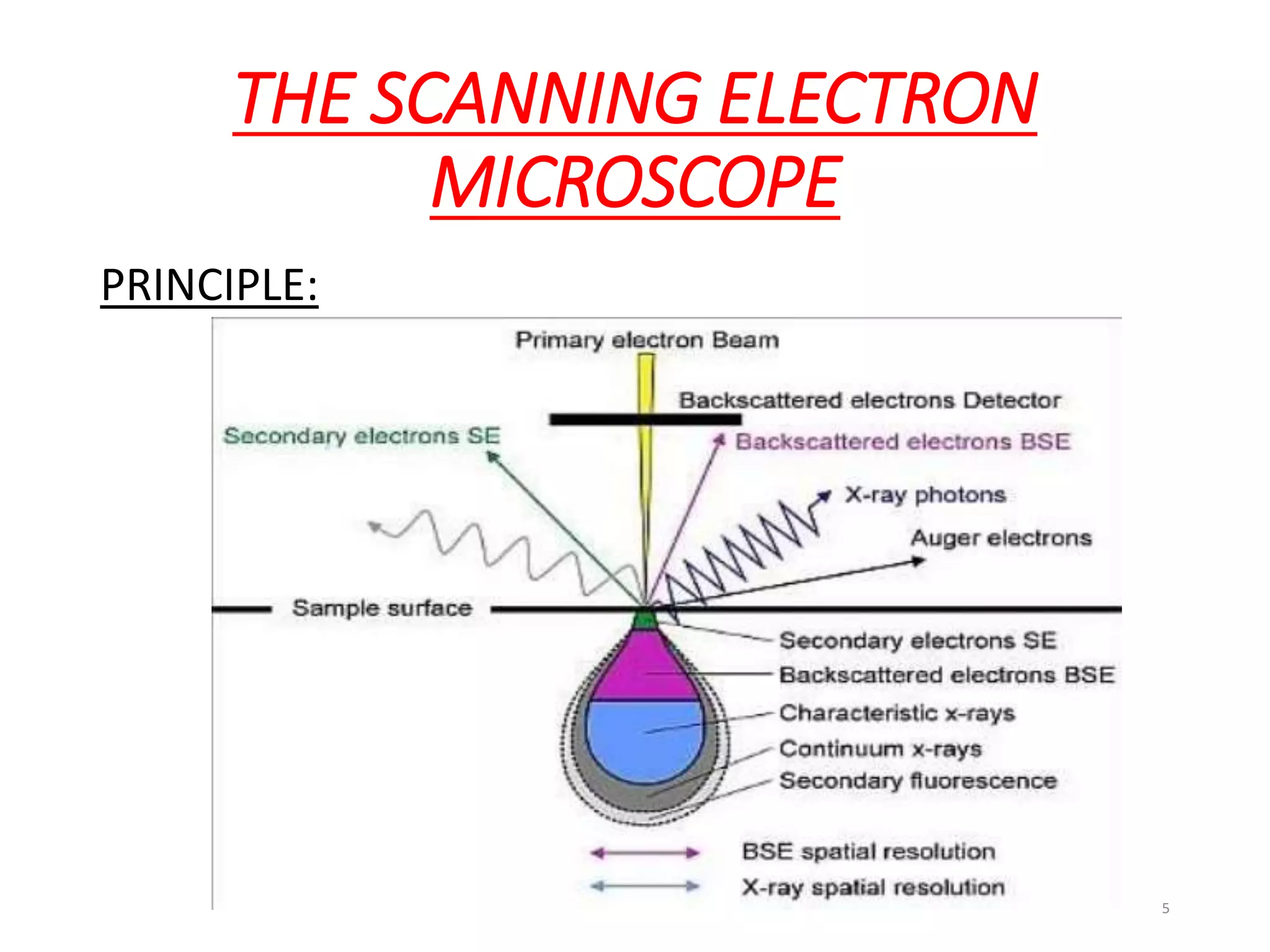
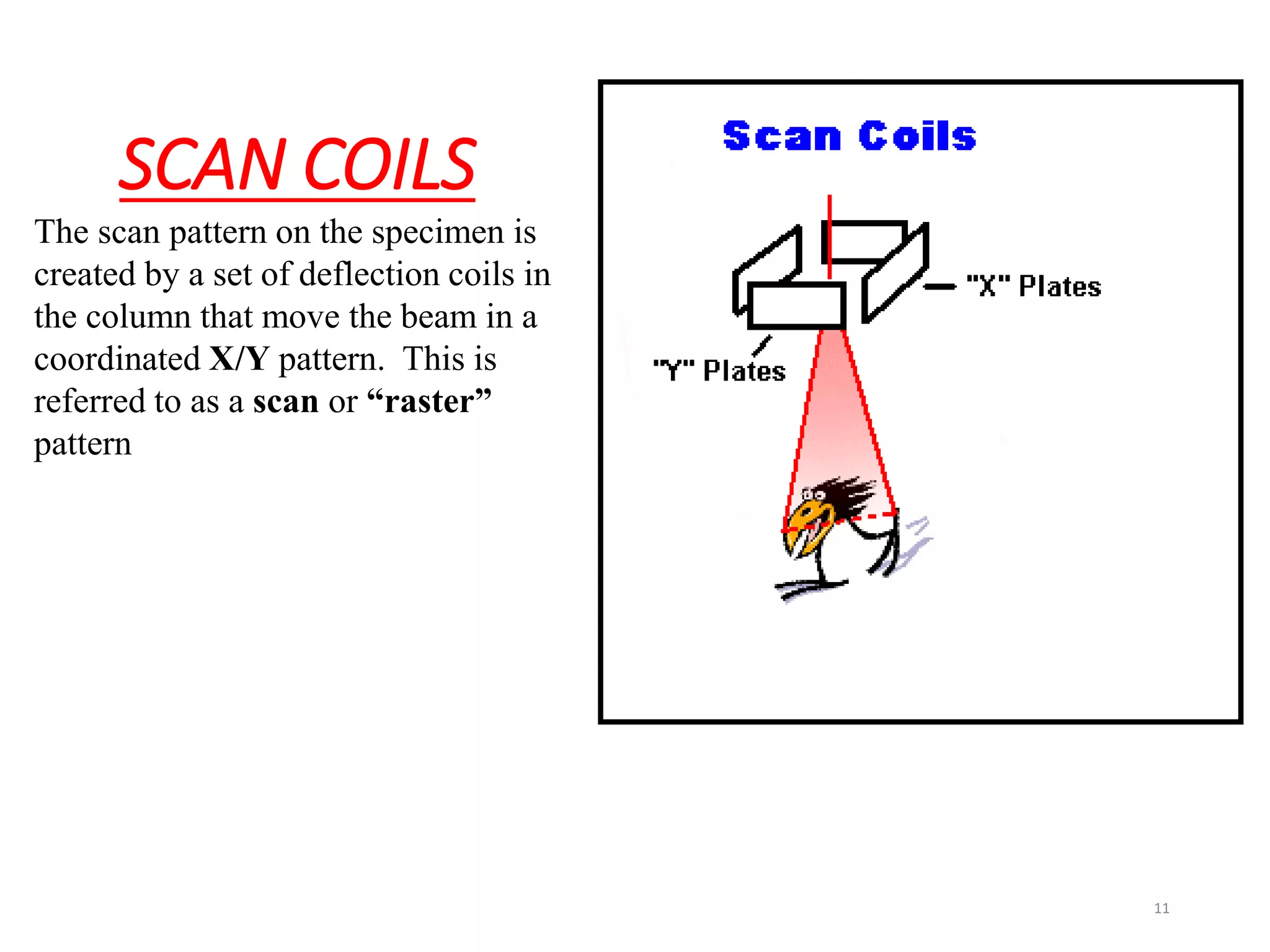
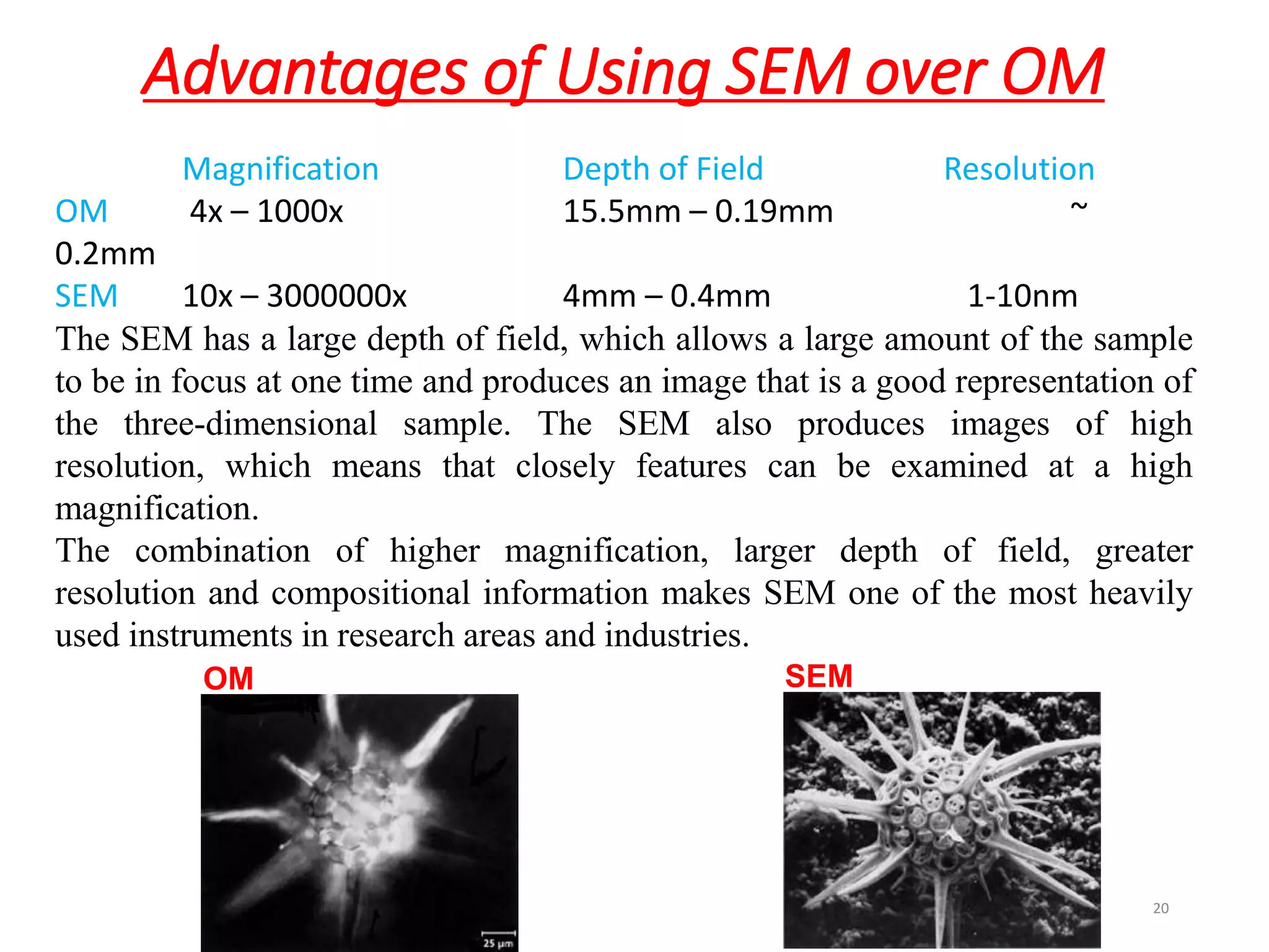
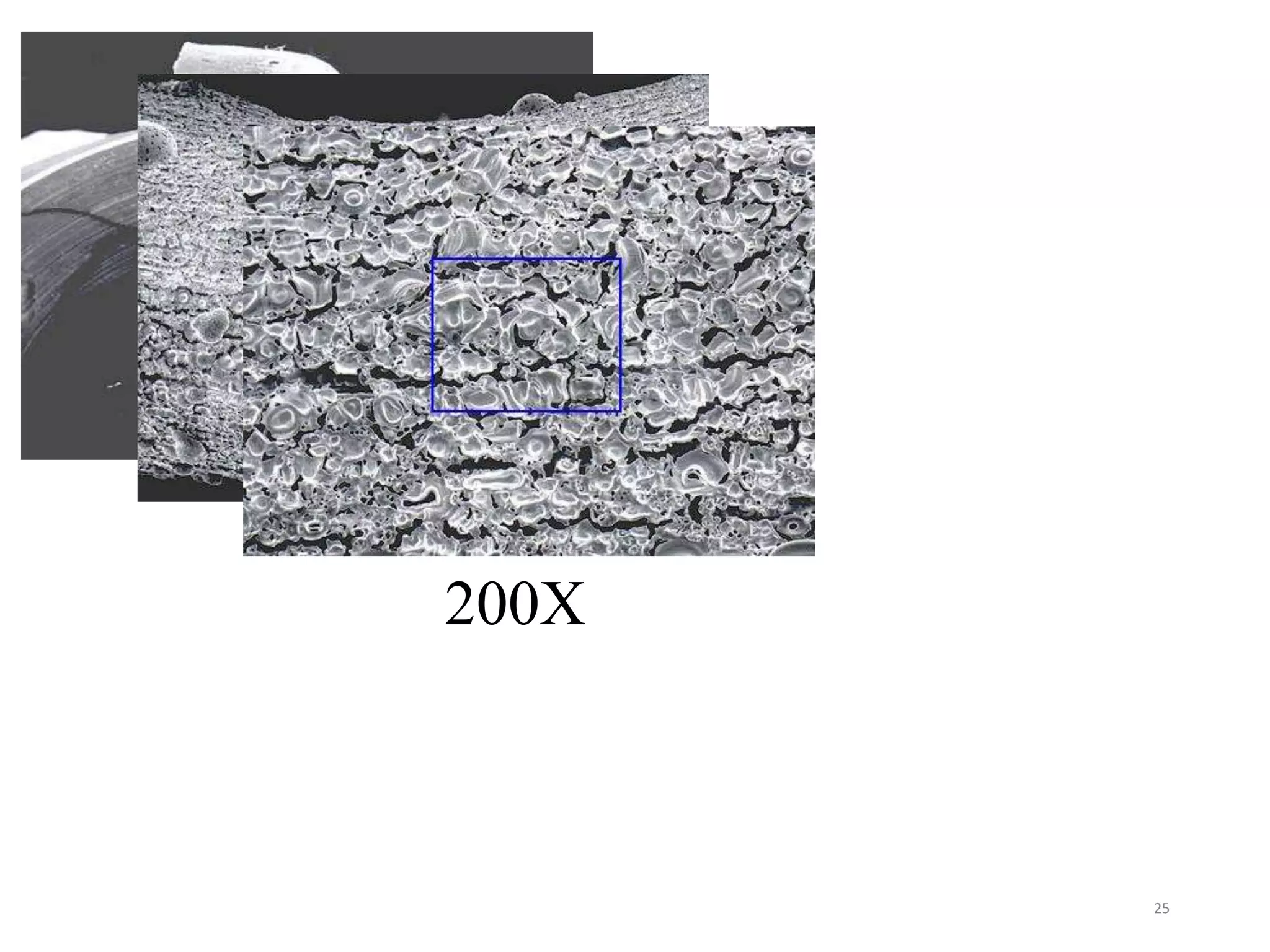
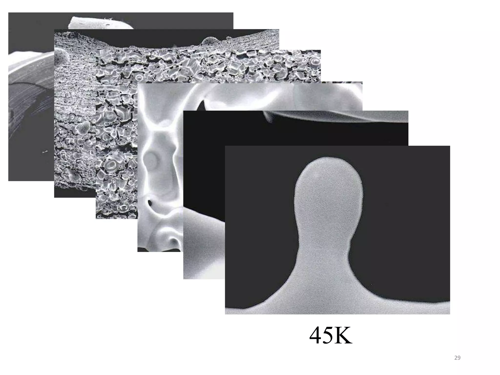
A PRESENTATION ON
“SCANNING ELECTRON MICROSCOPY”
1
Presented To:
Sir Ather Hassan
(Assistant Professor)
Presented by :
Kanwal Farooq Kayani
Roll NO:
BY700008
Course:
Experimental Techniques
M.Phil.(II) Spring 2020
Allama Iqbal Open University Islamabad .
Scanning Electron Microscope (SEM)
2
CONTENTS
 THE SCANNING ELECTRON MICROSCOPE
 PRINCIPLE
 CONSTRUCTION
 ADVANTAGES
 DISADVANTAGES
 APPLICATIONS
3
THE SCANNING ELECTRON
MICROSCOPE
4
THE SCANNING ELECTRON
MICROSCOPE
PRINCIPLE:
5
Construction
Basic Components are as following:
Electron gun(Filament)
Condenser Lenses
Scan Coils
Chamber
Detector
Computer Hardware and Software
6
Schematic View of
SEM
7
Electron Guns
• Two basic types of electron guns are available
•THERMIONIC GUNS
•FIELD EMISSION GUNS
THERMIONIC GUNS:
Which are the most common type, apply thermal energy to a filament to
coax electrons away from the gun and toward the specimen under
examination.
 Usually made of tungsten, which has a high melting point
8
Electron Guns
FIELD EMISSION GUNS:
Create a strong electrical field to pull electrons away from the atoms they are
associated with.
 Electron guns are located either at the very top or at the very bottom of an
SEM and fire a beam of electrons at the object under examination.
 These electrons don't naturally go where they need to, however, which gets
us to the next component of SEMs.
9
CONDENSER LENSES
Just like optical microscopes, SEMs use Condenser lenses to produce clear
and detailed images.
 The Condenser lenses in these devices, however, work differently.
 For one thing, they aren't made of glass.
Instead, the Condenser lenses are made of magnets capable of bending the
path of electrons.
 By doing so, the Condenser lenses focus and control the electron beam,
ensuring that the electrons end up precisely where they need to go.
10
SCAN COILS
The scan pattern on the specimen is
created by a set of deflection coils in
the column that move the beam in a
coordinated X/Y pattern. This is
referred to as a scan or “raster”
pattern
11
CHAMBER
 The sample chamber of an SEM is where researchers place the specimen
that they are examining.
In fact, SEMs are so sensitive to vibrations that they are often installed on
the ground floor of a building.
They also manipulate the specimen, placing it at different angles and moving
it so that researchers don't have to constantly remount the object to take
different images.
12
Signals from the sample
13
Incoming electrons
Secondary electrons
Backscattered
electrons
Auger electrons
X-rays
Cathodo-
luminescence (light)
Sample
DETECTORS
 Various types of detectors are there in SEM.
 These devices detect the various ways that the electron beam interacts with
the sample object.
 For instance, Everhart-Thornley detectors register secondary electrons,
which are electrons dislodged from the outer surface of a specimen. These
detectors are capable of producing the most detailed images of an object's
surface.
 Other detectors, such as backscattered electron detectors and X-ray
detectors, can tell researchers about the composition of a substance.
14
VACCUM CHAMBER
 SEMs require a vacuum to operate.
 Without a vacuum, the electron beam generated by the electron gun would
encounter constant interference from air particles in the atmosphere.
 Not only would these particles block the path of the electron beam, they
would also be knocked out of the air and onto the specimen, which would
distort the surface of the specimen.
15
HOW THE SEM WORKS?
The SEM uses electrons instead of light to form an image.
A beam of electrons is produced at the top of the microscope by heating of a
metallic filament
The electron beam follows a vertical path through the column of the
microscope. It makes its way through electromagnetic lenses which focus
and direct the beam down towards the sample.
Once it hits the sample, other electrons ( backscattered or secondary ) are
ejected from the sample.
Detectors collect the secondary or backscattered electrons, and convert them
to a signal that is sent to a viewing screen similar to the one in an ordinary
television, producing an image.
16
17
CHARACTERISTIC INFORMATION: SEM
Topography:
The surface features of an object or "how it looks", its texture; direct relation
between these features and materials properties
Morphology:
The shape and size of the particles making up the object; direct relation
between these structures and materials properties
Composition:
The elements and compounds that the object is composed of and the relative
amounts of them; direct relationship between composition and materials
properties
Crystallographic Information:
How the atoms are arranged in the object; direct relation between these
arrangements and material properties.
18
ADVANTAGES
 Advantages of a Scanning Electron Microscope include its wide-array of
applications, the detailed three-dimensional and topographical imaging and
the versatile information garnered from different detectors.
 SEMs are also easy to operate with the proper training and advances in
computer technology and associated software make operation user-friendly.
 Although all samples must be prepared before placed in the vacuum
chamber, most SEM samples require minimal preparation actions.
19
Advantages of Using SEM over OM
20
Magnification Depth of Field Resolution
OM 4x – 1000x 15.5mm – 0.19mm ~
0.2mm
SEM 10x – 3000000x 4mm – 0.4mm 1-10nm
The SEM has a large depth of field, which allows a large amount of the sample
to be in focus at one time and produces an image that is a good representation of
the three-dimensional sample. The SEM also produces images of high
resolution, which means that closely features can be examined at a high
magnification.
The combination of higher magnification, larger depth of field, greater
resolution and compositional information makes SEM one of the most heavily
used instruments in research areas and industries.
OM SEM
DISADVANTAGES
The disadvantages of a Scanning Electron Microscope start with the size and
cost.
 SEMs are expensive, large and must be housed in an area free of any
possible electric, magnetic or vibration interference.
 Maintenance involves keeping a steady voltage, currents to electromagnetic
coils and circulation of cool water.
 SEMs are limited to solid, inorganic samples small enough to fit inside the
vacuum chamber that can handle moderate vacuum pressure.
21
APPLICATIONS
SEMs have a variety of applications in a number of scientific and industry-
related fields, especially where characterizations of solid materials is
beneficial.
 In addition to topographical, morphological and compositional information,
a Scanning Electron Microscope can detect and analyze surface fractures,
provide information in microstructures, examine surface contaminations,
reveal spatial variations in chemical compositions, provide qualitative
chemical analyses and identify crystalline structures.
In addition, SEMs have practical industrial and technological applications
such as semiconductor inspection, production line of miniscule products and
assembly of microchips for computers.
 SEMs can be as essential research tool in fields such as life science,
biology, gemology, medical and forensic science, metallurgy.
22
10X
23
110X
24
200X
25
400X
26
4K
27
16K
28
45K
29
Thank You
30

Sem (2)

  • 1.
    A PRESENTATION ON “SCANNINGELECTRON MICROSCOPY” 1 Presented To: Sir Ather Hassan (Assistant Professor) Presented by : Kanwal Farooq Kayani Roll NO: BY700008 Course: Experimental Techniques M.Phil.(II) Spring 2020 Allama Iqbal Open University Islamabad .
  • 2.
  • 3.
    CONTENTS  THE SCANNINGELECTRON MICROSCOPE  PRINCIPLE  CONSTRUCTION  ADVANTAGES  DISADVANTAGES  APPLICATIONS 3
  • 4.
  • 5.
  • 6.
    Construction Basic Components areas following: Electron gun(Filament) Condenser Lenses Scan Coils Chamber Detector Computer Hardware and Software 6
  • 7.
  • 8.
    Electron Guns • Twobasic types of electron guns are available •THERMIONIC GUNS •FIELD EMISSION GUNS THERMIONIC GUNS: Which are the most common type, apply thermal energy to a filament to coax electrons away from the gun and toward the specimen under examination.  Usually made of tungsten, which has a high melting point 8
  • 9.
    Electron Guns FIELD EMISSIONGUNS: Create a strong electrical field to pull electrons away from the atoms they are associated with.  Electron guns are located either at the very top or at the very bottom of an SEM and fire a beam of electrons at the object under examination.  These electrons don't naturally go where they need to, however, which gets us to the next component of SEMs. 9
  • 10.
    CONDENSER LENSES Just likeoptical microscopes, SEMs use Condenser lenses to produce clear and detailed images.  The Condenser lenses in these devices, however, work differently.  For one thing, they aren't made of glass. Instead, the Condenser lenses are made of magnets capable of bending the path of electrons.  By doing so, the Condenser lenses focus and control the electron beam, ensuring that the electrons end up precisely where they need to go. 10
  • 11.
    SCAN COILS The scanpattern on the specimen is created by a set of deflection coils in the column that move the beam in a coordinated X/Y pattern. This is referred to as a scan or “raster” pattern 11
  • 12.
    CHAMBER  The samplechamber of an SEM is where researchers place the specimen that they are examining. In fact, SEMs are so sensitive to vibrations that they are often installed on the ground floor of a building. They also manipulate the specimen, placing it at different angles and moving it so that researchers don't have to constantly remount the object to take different images. 12
  • 13.
    Signals from thesample 13 Incoming electrons Secondary electrons Backscattered electrons Auger electrons X-rays Cathodo- luminescence (light) Sample
  • 14.
    DETECTORS  Various typesof detectors are there in SEM.  These devices detect the various ways that the electron beam interacts with the sample object.  For instance, Everhart-Thornley detectors register secondary electrons, which are electrons dislodged from the outer surface of a specimen. These detectors are capable of producing the most detailed images of an object's surface.  Other detectors, such as backscattered electron detectors and X-ray detectors, can tell researchers about the composition of a substance. 14
  • 15.
    VACCUM CHAMBER  SEMsrequire a vacuum to operate.  Without a vacuum, the electron beam generated by the electron gun would encounter constant interference from air particles in the atmosphere.  Not only would these particles block the path of the electron beam, they would also be knocked out of the air and onto the specimen, which would distort the surface of the specimen. 15
  • 16.
    HOW THE SEMWORKS? The SEM uses electrons instead of light to form an image. A beam of electrons is produced at the top of the microscope by heating of a metallic filament The electron beam follows a vertical path through the column of the microscope. It makes its way through electromagnetic lenses which focus and direct the beam down towards the sample. Once it hits the sample, other electrons ( backscattered or secondary ) are ejected from the sample. Detectors collect the secondary or backscattered electrons, and convert them to a signal that is sent to a viewing screen similar to the one in an ordinary television, producing an image. 16
  • 17.
  • 18.
    CHARACTERISTIC INFORMATION: SEM Topography: Thesurface features of an object or "how it looks", its texture; direct relation between these features and materials properties Morphology: The shape and size of the particles making up the object; direct relation between these structures and materials properties Composition: The elements and compounds that the object is composed of and the relative amounts of them; direct relationship between composition and materials properties Crystallographic Information: How the atoms are arranged in the object; direct relation between these arrangements and material properties. 18
  • 19.
    ADVANTAGES  Advantages ofa Scanning Electron Microscope include its wide-array of applications, the detailed three-dimensional and topographical imaging and the versatile information garnered from different detectors.  SEMs are also easy to operate with the proper training and advances in computer technology and associated software make operation user-friendly.  Although all samples must be prepared before placed in the vacuum chamber, most SEM samples require minimal preparation actions. 19
  • 20.
    Advantages of UsingSEM over OM 20 Magnification Depth of Field Resolution OM 4x – 1000x 15.5mm – 0.19mm ~ 0.2mm SEM 10x – 3000000x 4mm – 0.4mm 1-10nm The SEM has a large depth of field, which allows a large amount of the sample to be in focus at one time and produces an image that is a good representation of the three-dimensional sample. The SEM also produces images of high resolution, which means that closely features can be examined at a high magnification. The combination of higher magnification, larger depth of field, greater resolution and compositional information makes SEM one of the most heavily used instruments in research areas and industries. OM SEM
  • 21.
    DISADVANTAGES The disadvantages ofa Scanning Electron Microscope start with the size and cost.  SEMs are expensive, large and must be housed in an area free of any possible electric, magnetic or vibration interference.  Maintenance involves keeping a steady voltage, currents to electromagnetic coils and circulation of cool water.  SEMs are limited to solid, inorganic samples small enough to fit inside the vacuum chamber that can handle moderate vacuum pressure. 21
  • 22.
    APPLICATIONS SEMs have avariety of applications in a number of scientific and industry- related fields, especially where characterizations of solid materials is beneficial.  In addition to topographical, morphological and compositional information, a Scanning Electron Microscope can detect and analyze surface fractures, provide information in microstructures, examine surface contaminations, reveal spatial variations in chemical compositions, provide qualitative chemical analyses and identify crystalline structures. In addition, SEMs have practical industrial and technological applications such as semiconductor inspection, production line of miniscule products and assembly of microchips for computers.  SEMs can be as essential research tool in fields such as life science, biology, gemology, medical and forensic science, metallurgy. 22
  • 23.
  • 24.
  • 25.
  • 26.
  • 27.
  • 28.
  • 29.
  • 30.