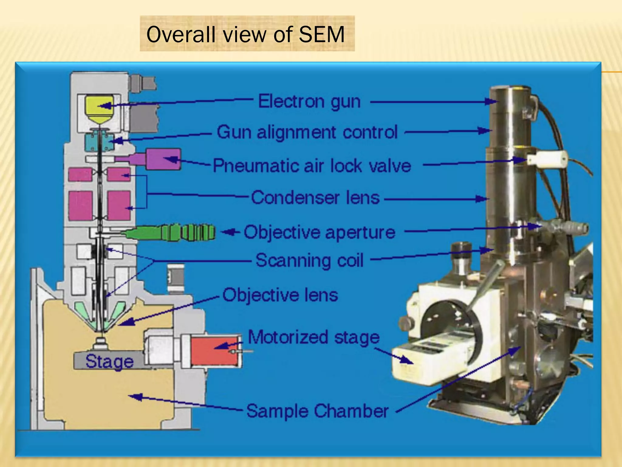
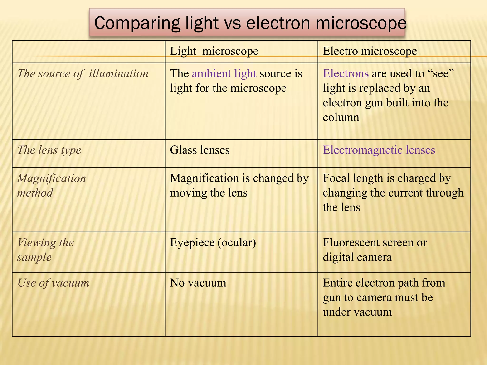
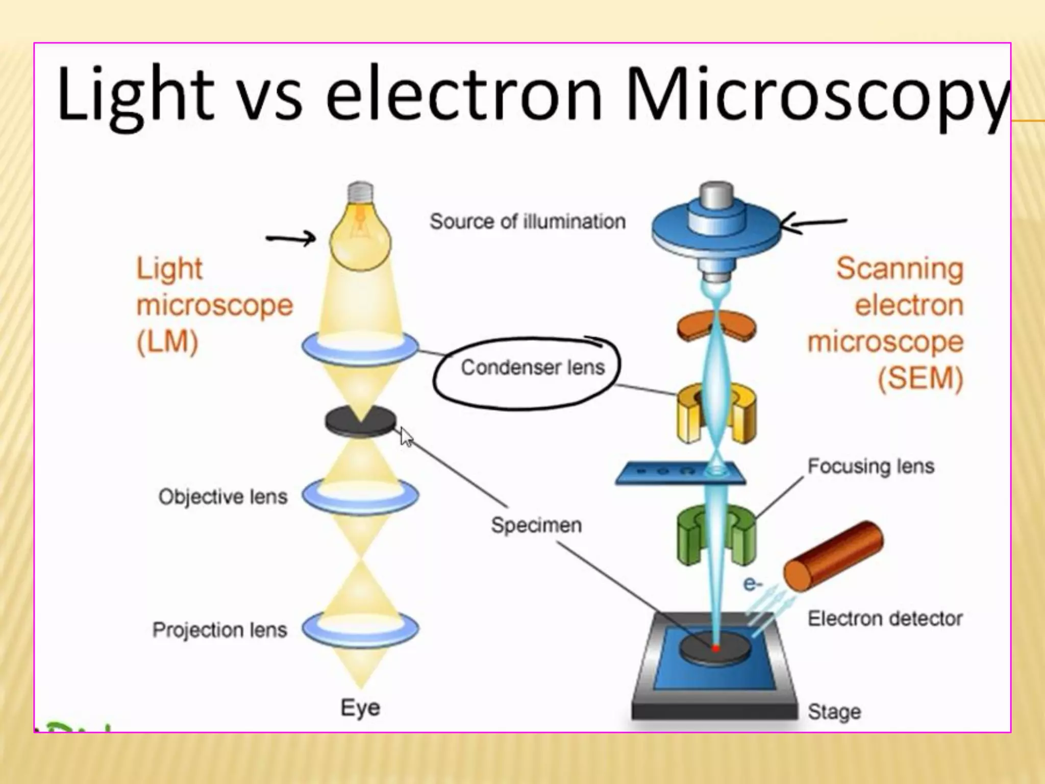
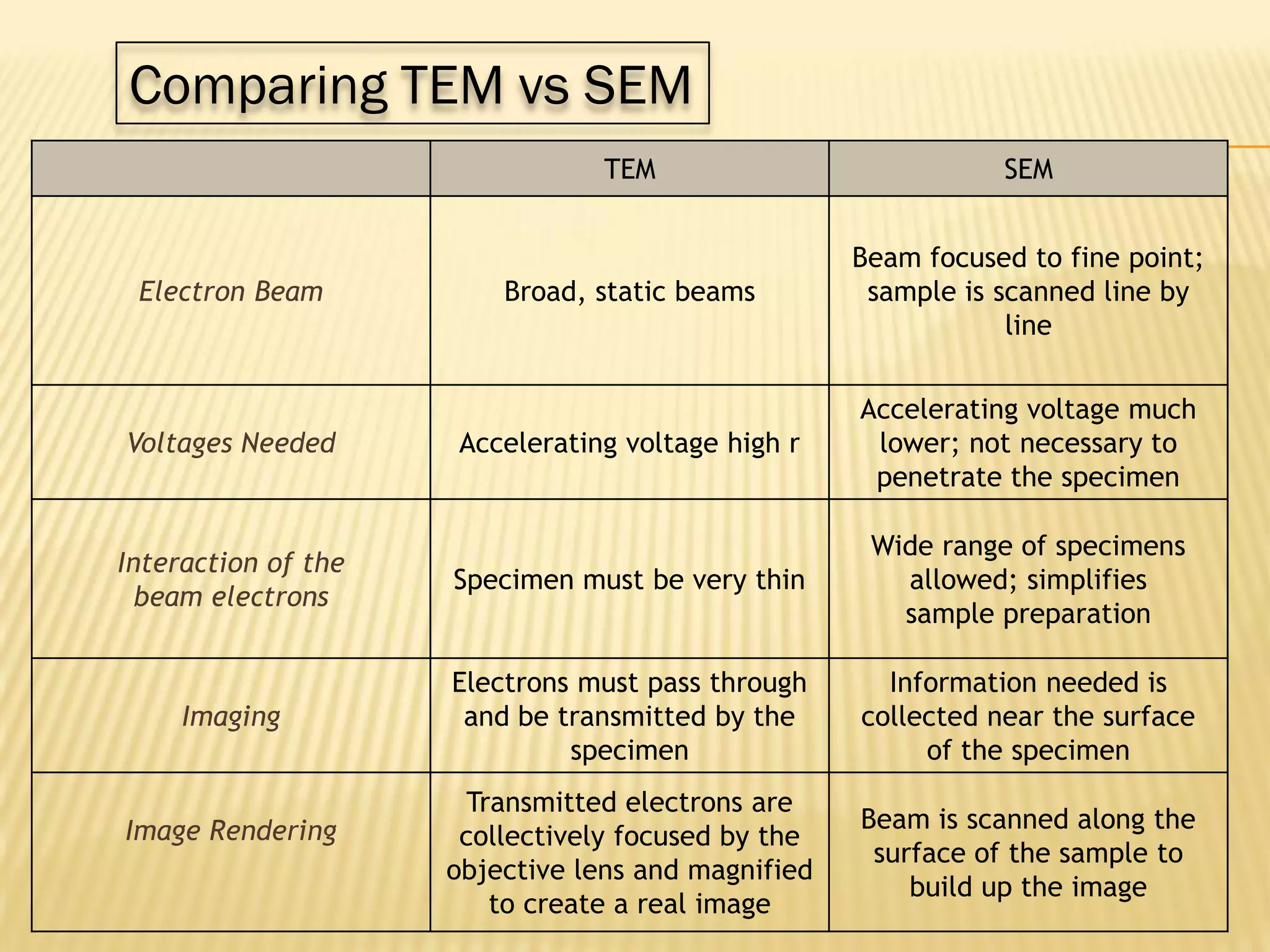
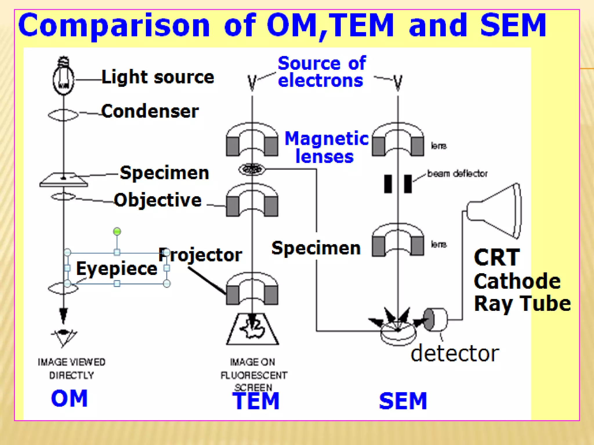
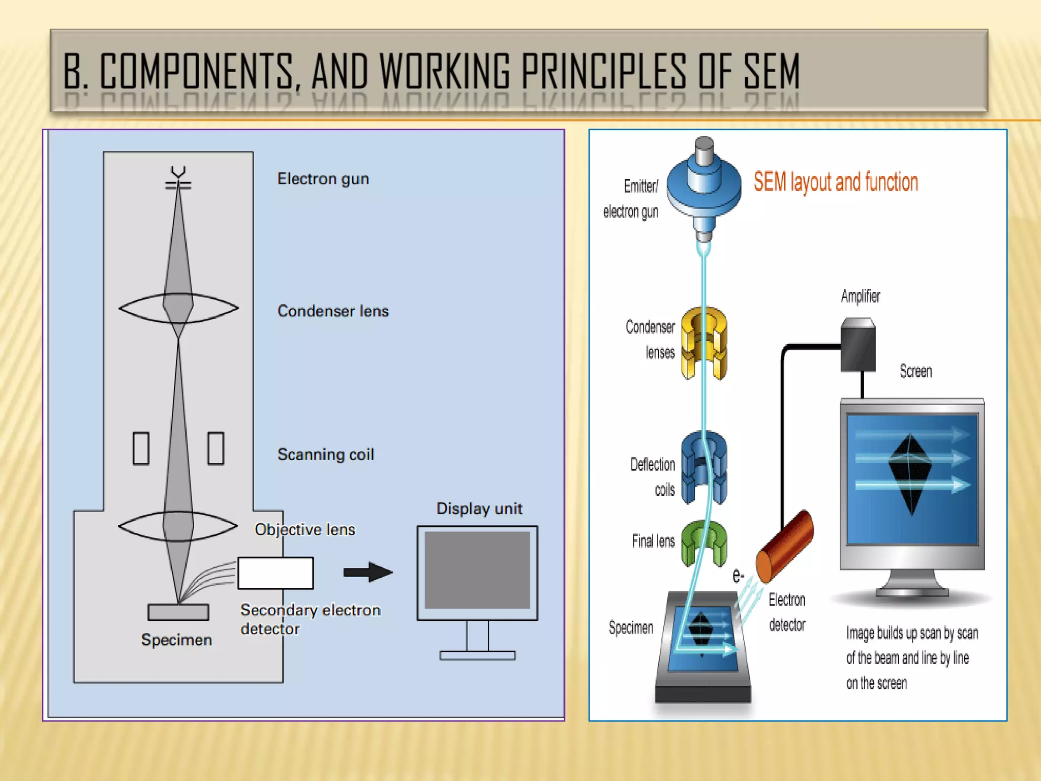
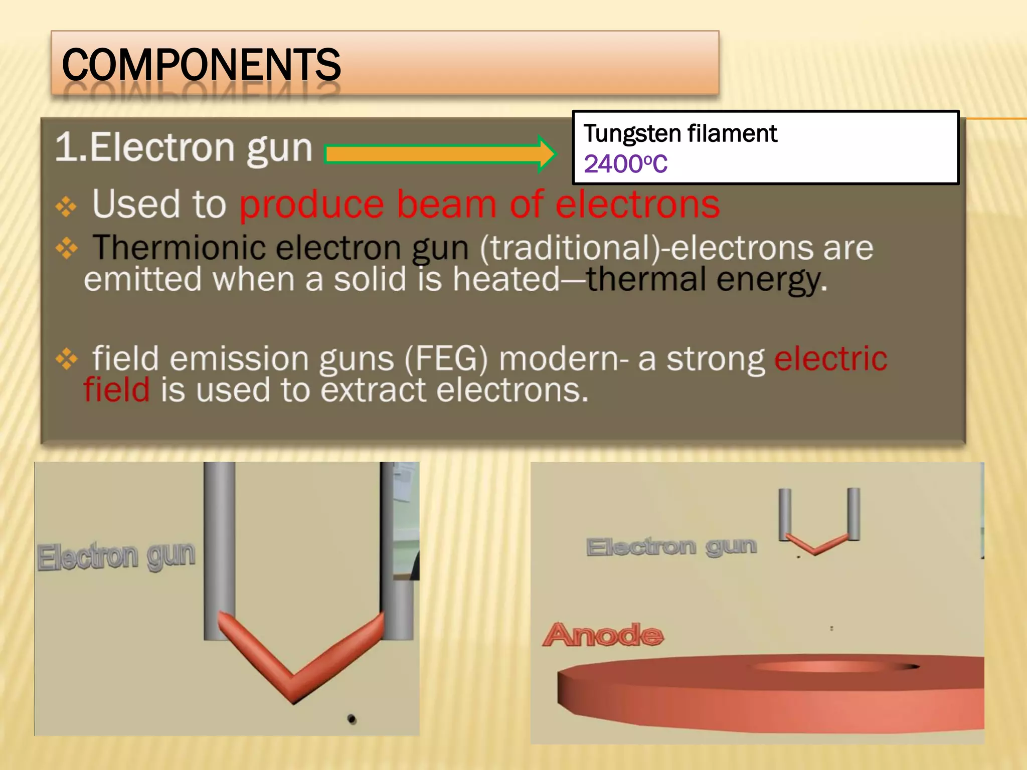
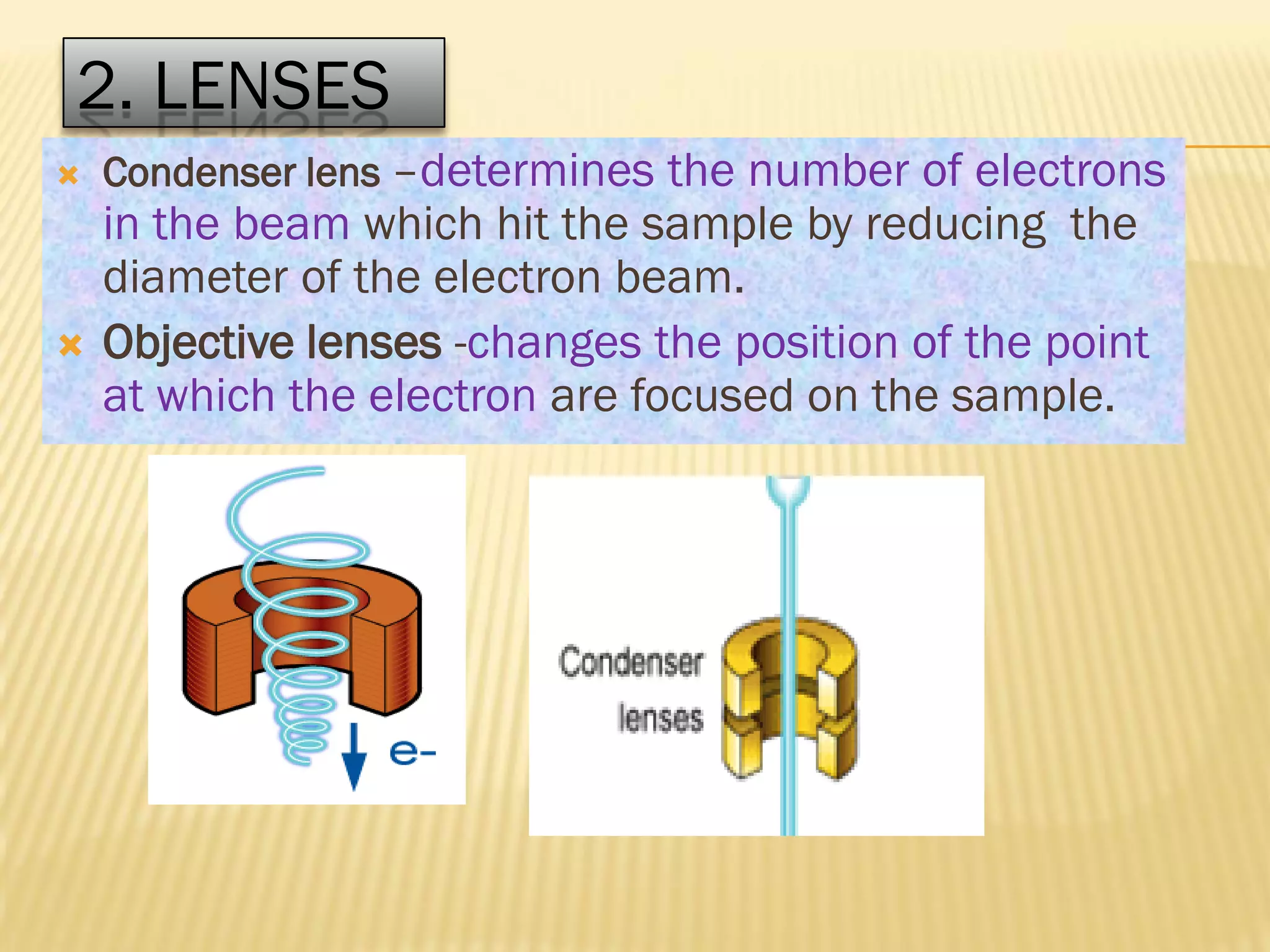
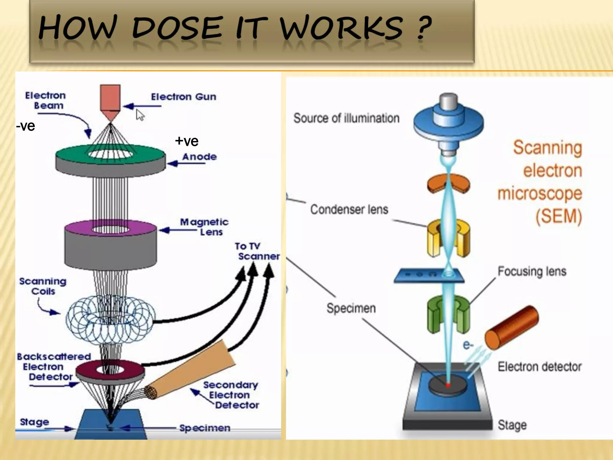
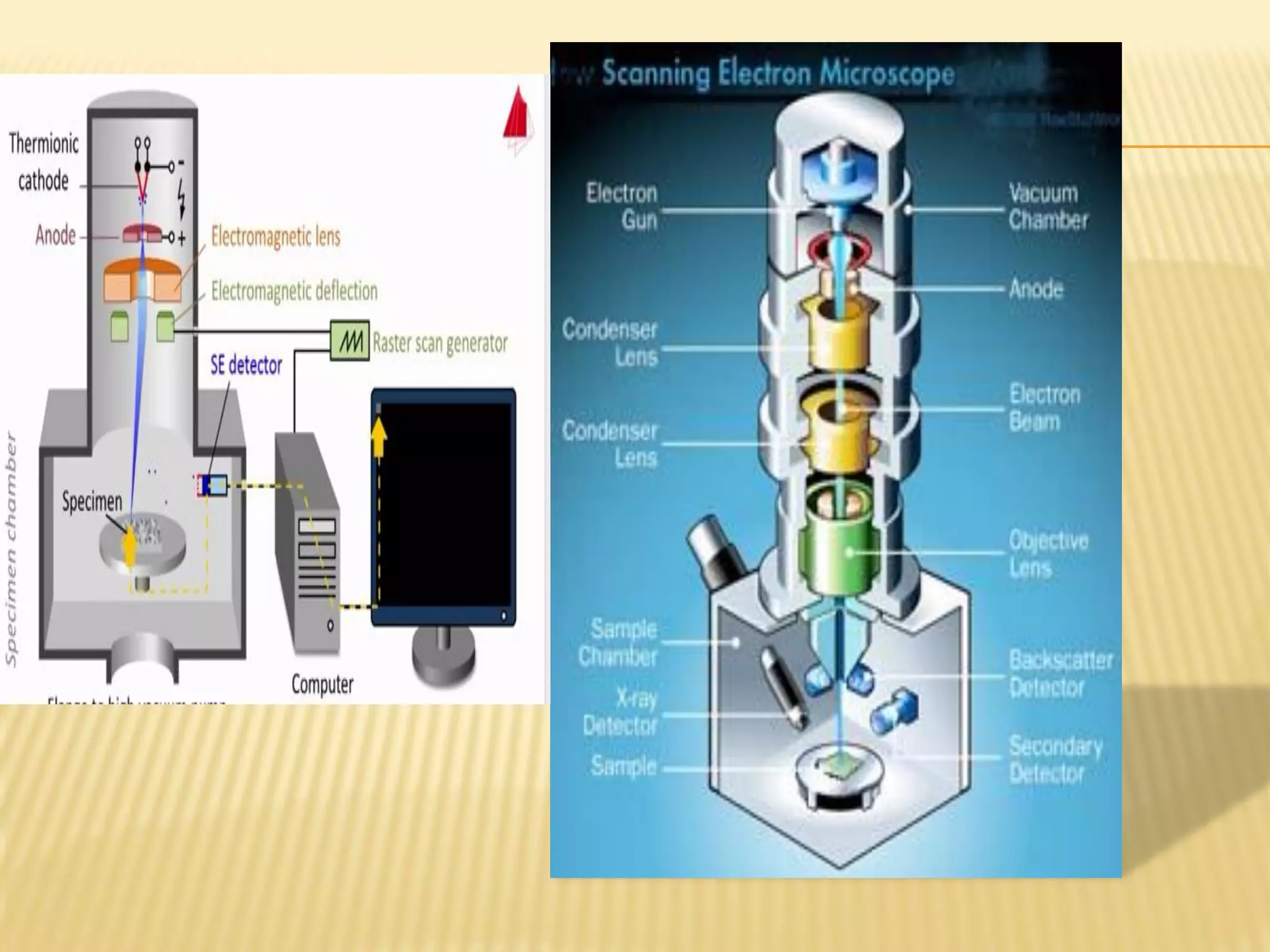
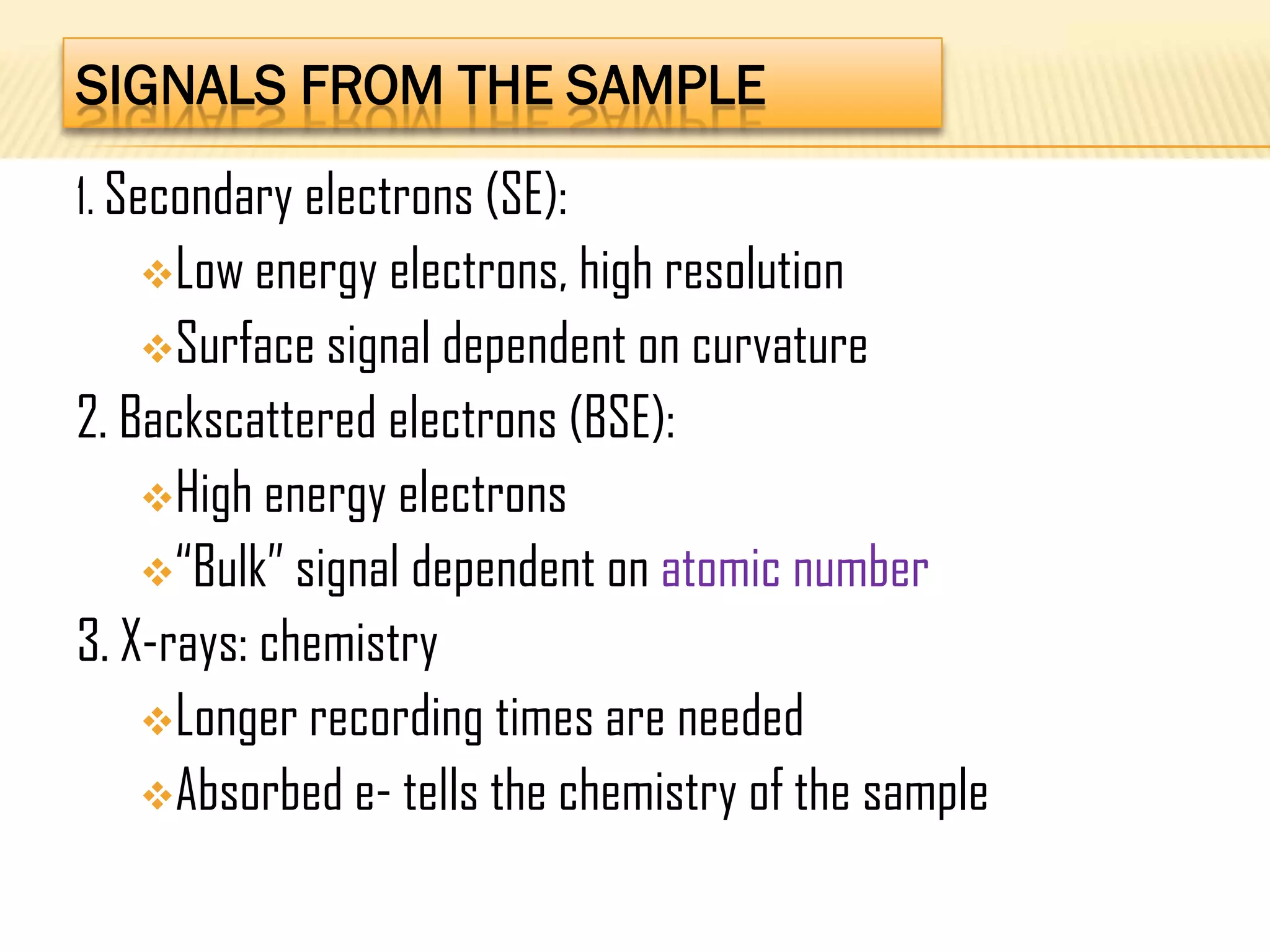
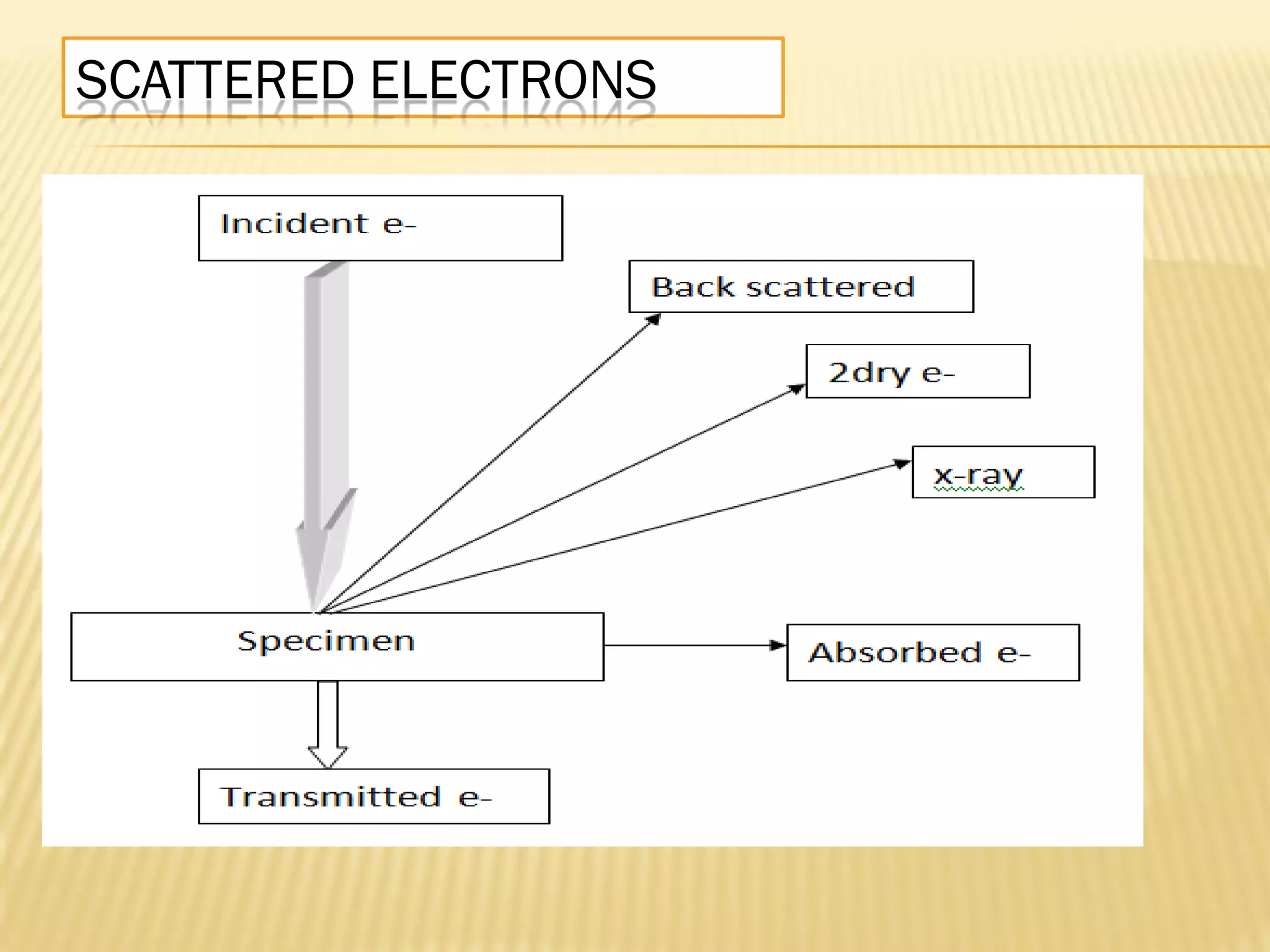
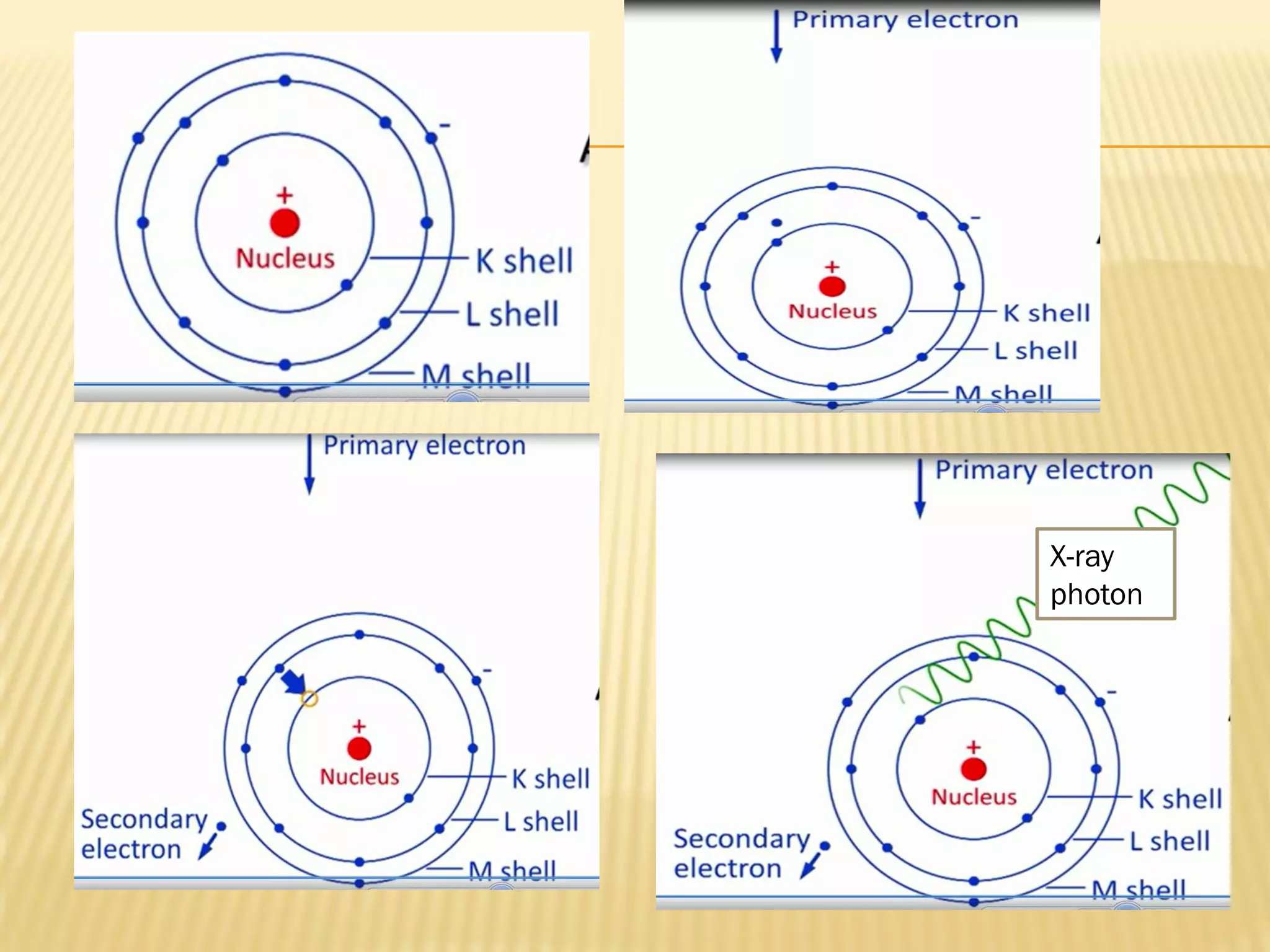
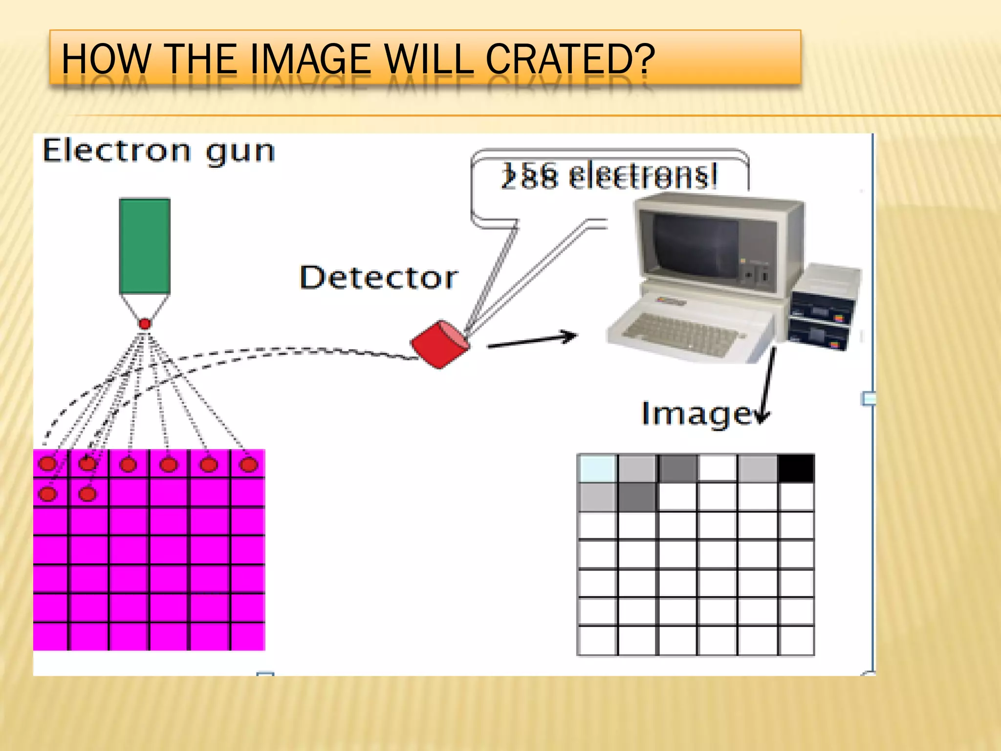
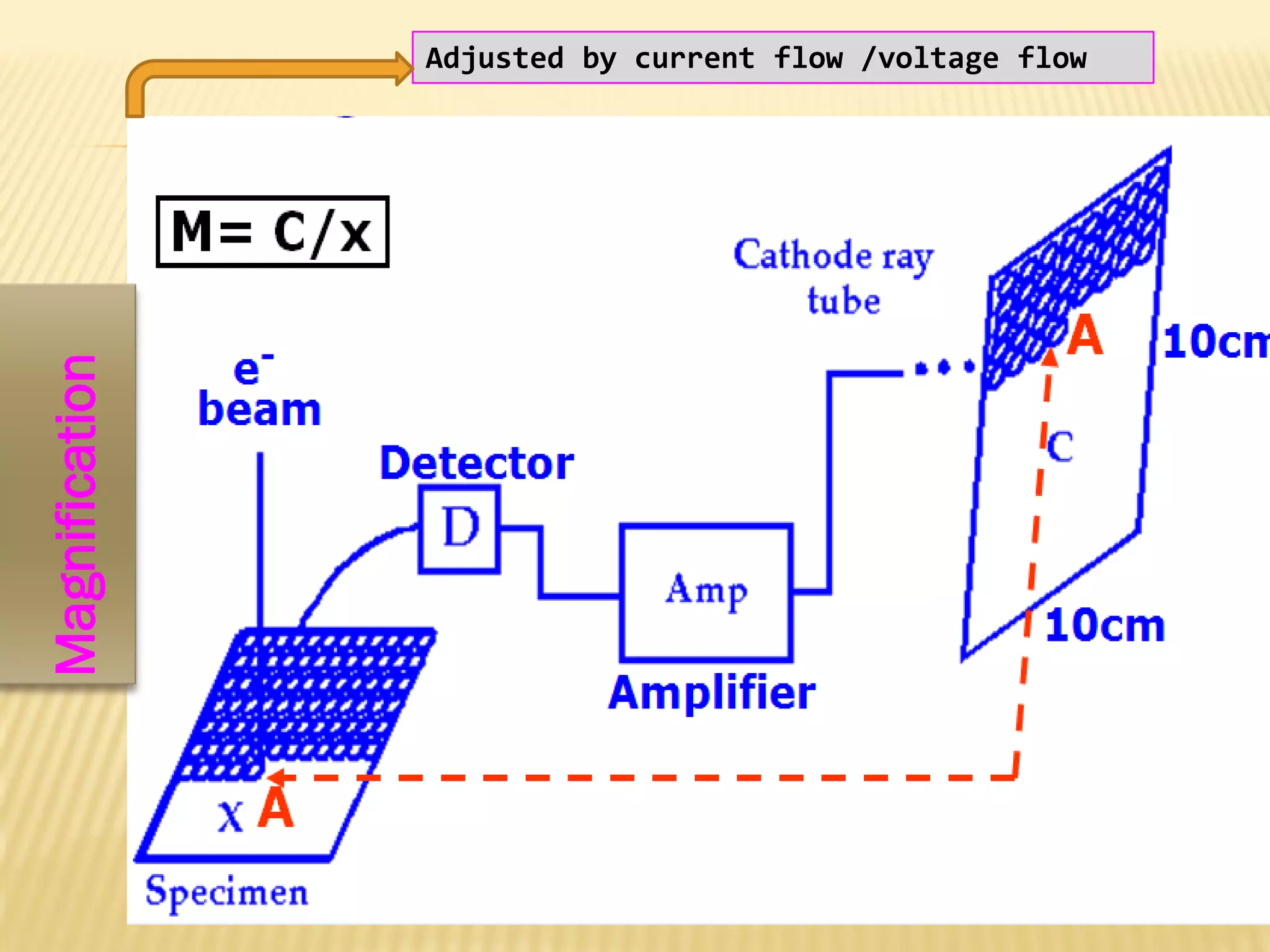
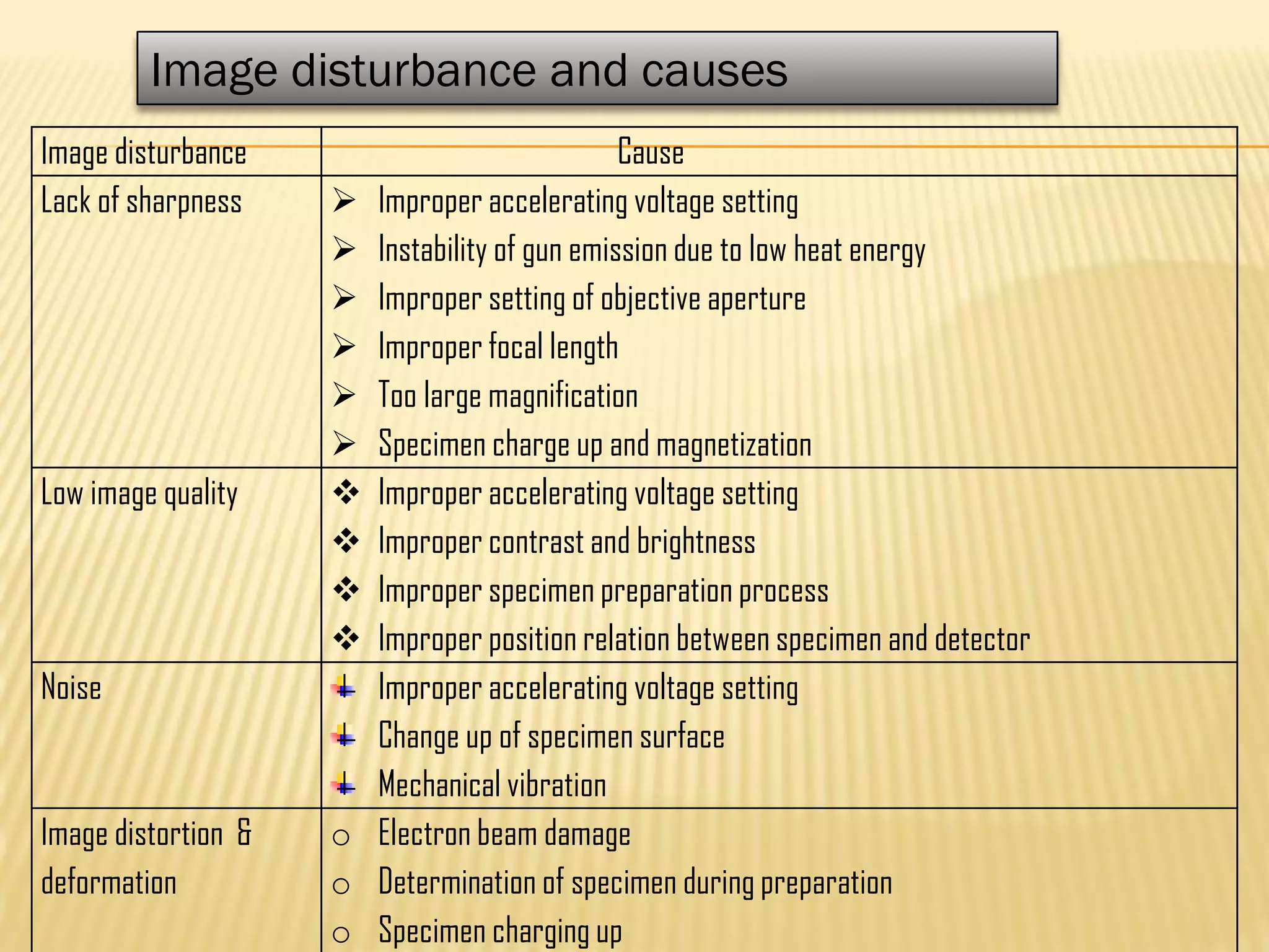
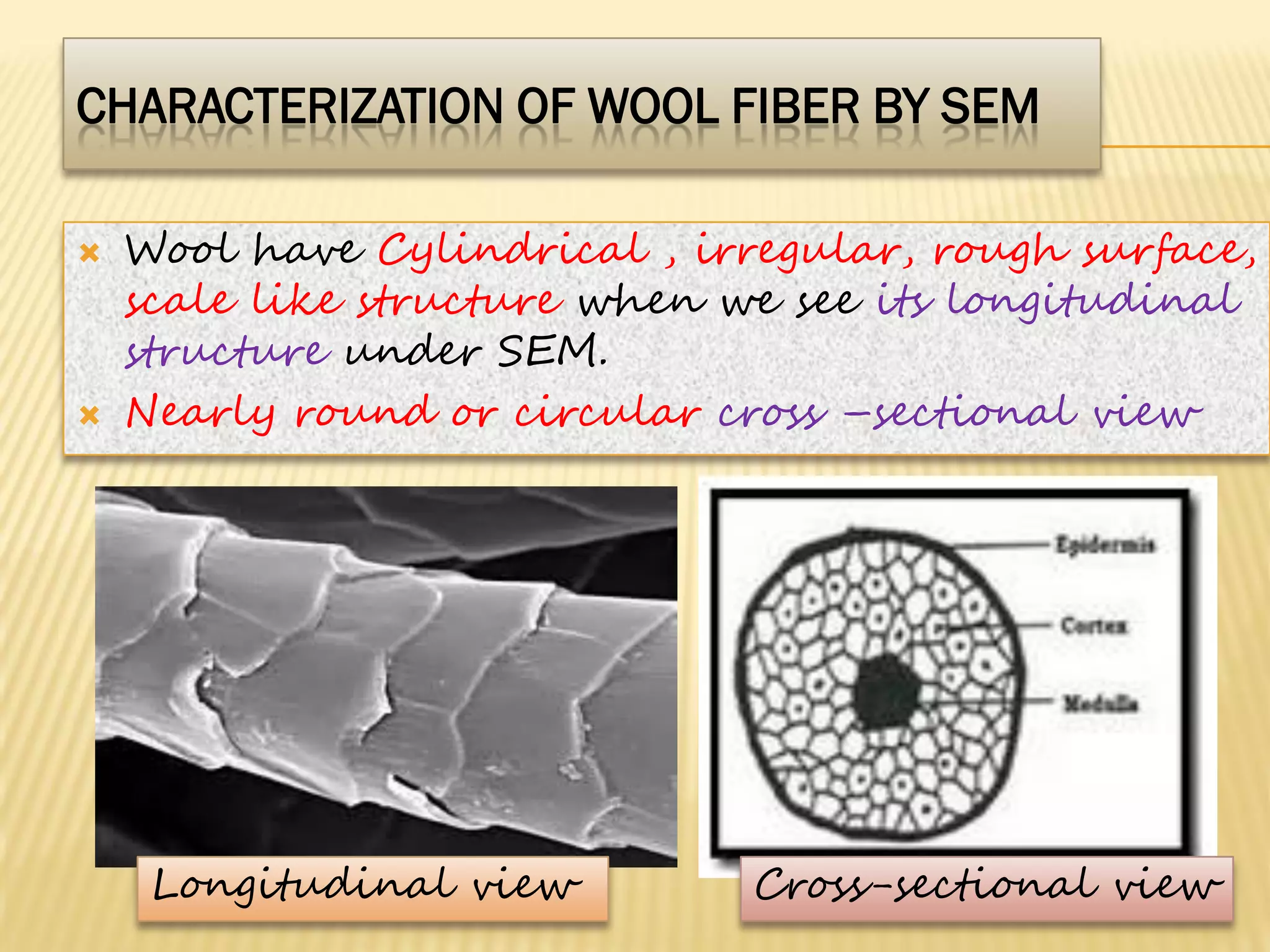
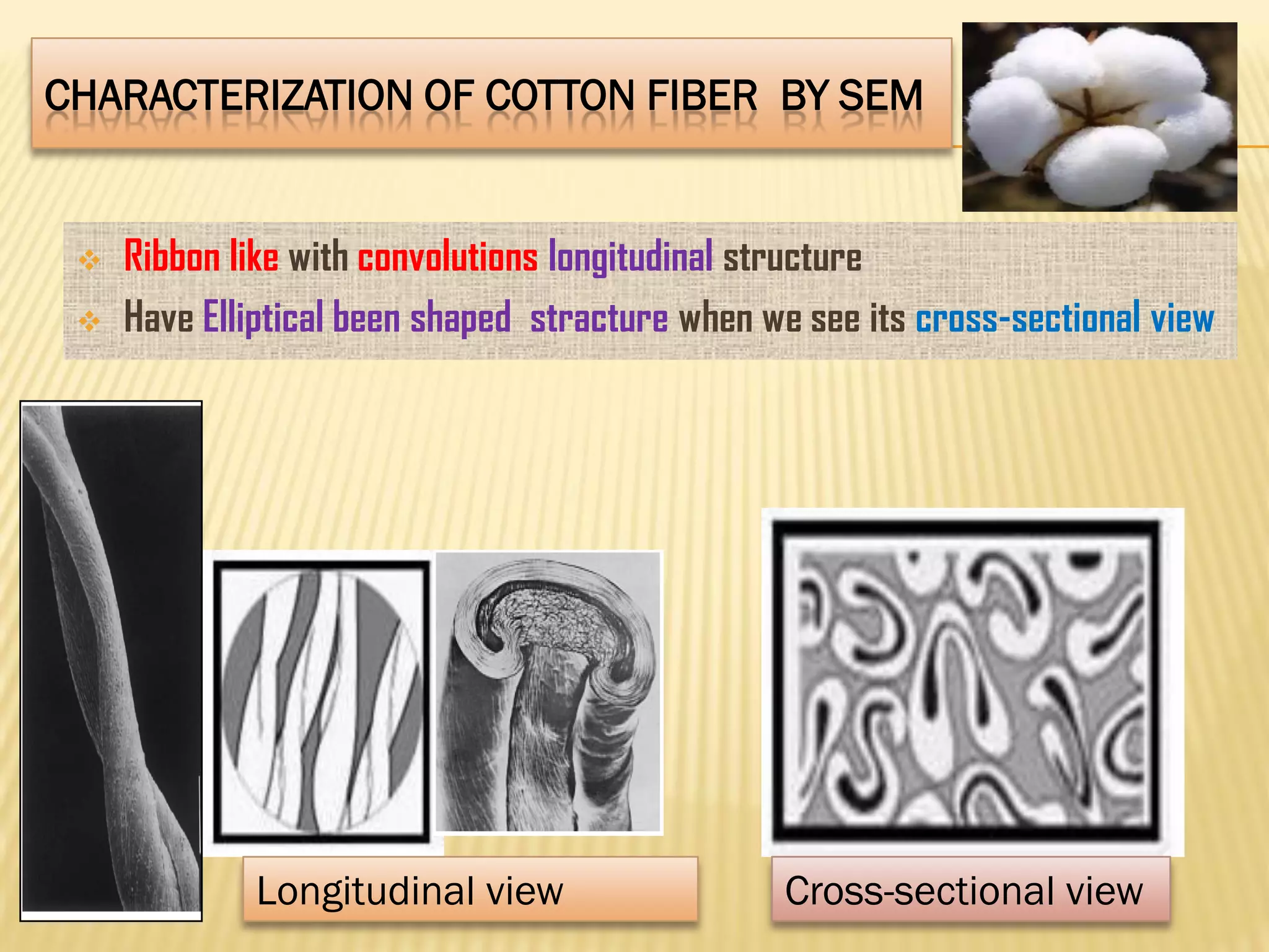
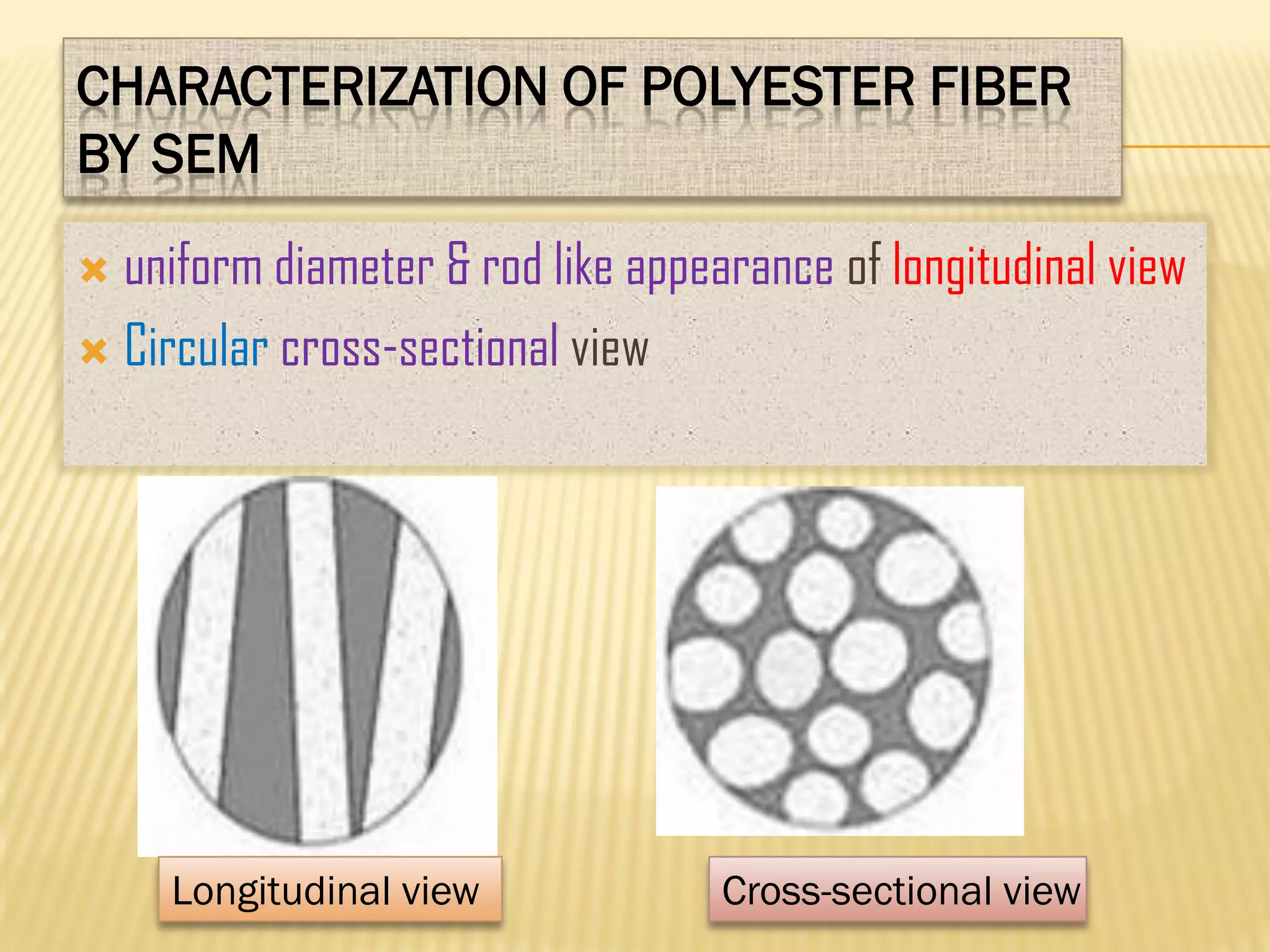
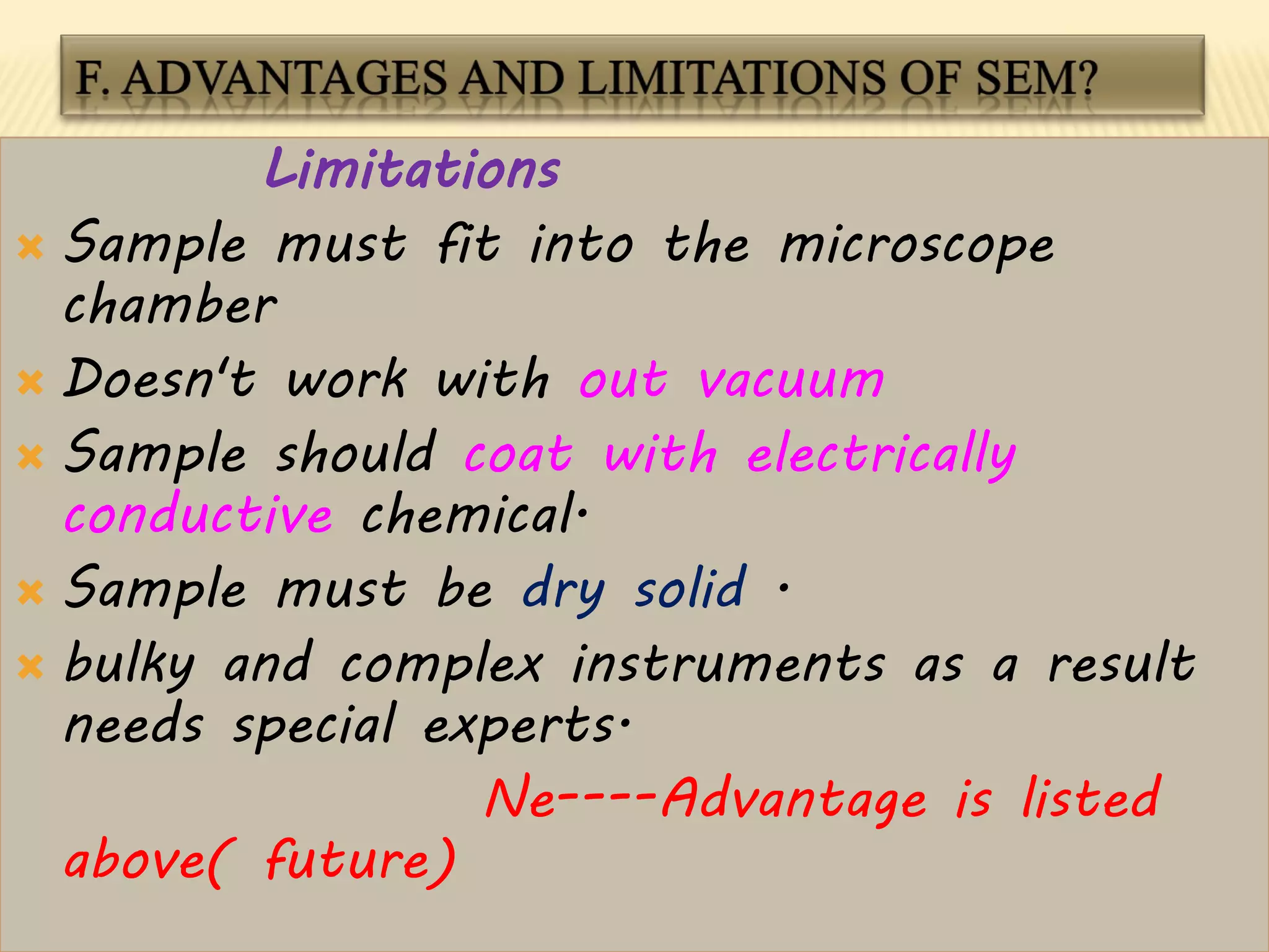
DIRE DAWA INSTITUTE OF TECHNOLOGY
DIRE DAWA UNIVERSITY
WORKING PRINCIPLE OF SCANNING
ELECTRON MICROSCOPE
BY : TAAME BERHANU
2018
FIBER CHARACTERIZATION USING
SCANNING ELECTRON MICROSCOPY (SEM)
OUTLINE
 Introduction
 Components, and working principles of SEM
 Salient futures of SEM
 Data analysis by SEM
 Textile fiber characterization by SEM
 Advantages and limitations of SEM?
Overall view of SEM
A. INTRODUCTION
Type of electron microscope that images the sample by
scanning it with high energy beam of electrons .
What can we study in a SEM?
o Topography and morphology(texture)
o Chemistry(chemical composition)
o Crystallography
o Orientation of materials
Designed by Stinzing and Knoll in Germany in the early 25s
1965.
Light microscope Electro microscope
The source of illumination The ambient light source is
light for the microscope
Electrons are used to “see”
light is replaced by an
electron gun built into the
column
The lens type Glass lenses Electromagnetic lenses
Magnification
method
Magnification is changed by
moving the lens
Focal length is charged by
changing the current through
the lens
Viewing the
sample
Eyepiece (ocular) Fluorescent screen or
digital camera
Use of vacuum No vacuum Entire electron path from
gun to camera must be
under vacuum
Comparing light vs electron microscope
TEM SEM
Electron Beam Broad, static beams
Beam focused to fine point;
sample is scanned line by
line
Voltages Needed Accelerating voltage high r
Accelerating voltage much
lower; not necessary to
penetrate the specimen
Interaction of the
beam electrons
Specimen must be very thin
Wide range of specimens
allowed; simplifies
sample preparation
Imaging
Electrons must pass through
and be transmitted by the
specimen
Information needed is
collected near the surface
of the specimen
Image Rendering
Transmitted electrons are
collectively focused by the
objective lens and magnified
to create a real image
Beam is scanned along the
surface of the sample to
build up the image
Comparing TEM vs SEM
COMPONENTS
Tungsten filament
2400oC
2. LENSES
 Condenser lens –determines the number of electrons
in the beam which hit the sample by reducing the
diameter of the electron beam.
 Objective lenses -changes the position of the point
at which the electron are focused on the sample.
3. SCANNING COILS
 Are used to raster/scan the e-beam across the sample
surface
 The e-beam can be scanned in a rectangular raster across
the surface of the sample by means of a series of “scan
coils” situated above the objective lens.
4. SAMPLE CHAMBER
A place where the sample was mounted on.
5. DETECTORS
 detect the secondary and backscattered electrons.
Have +ve charge
6. VACUUM CHAMBER
 Used to protect the electronic beam from interference with air.
 control the number of electrons which reach the sample.
 control the final convergence angle of the electron beam onto
the sample
7. Aperture
+ve
-ve
SIGNALS FROM THE SAMPLE
1. Secondary electrons (SE):
Low energy electrons, high resolution
Surface signal dependent on curvature
2. Backscattered electrons (BSE):
High energy electrons
“Bulk” signal dependent on atomic number
3. X-rays: chemistry
Longer recording times are needed
Absorbed e- tells the chemistry of the sample
SCATTERED ELECTRONS
X-ray
photon
HOW THE IMAGE WILL CRATED?
Adjusted by current flow /voltage flow
Magnification
RESOLUTION IS DEPEND UP ON?
 Size of the electron spot &wavelength of the electrons .
 size of the interaction volume (material interacts with the
electron beam)
SAMPLE PREPARATION
 1) Remove all water, solvents, or other materials that
could vaporize while in the vacuum.
 2) Firmly mount all the samples.
 3) Non-metallic samples, such as plants,
and ceramics, should be coated with
electrically conductive materials.
Image disturbance and causes
Image disturbance Cause
Lack of sharpness  Improper accelerating voltage setting
 Instability of gun emission due to low heat energy
 Improper setting of objective aperture
 Improper focal length
 Too large magnification
 Specimen charge up and magnetization
Low image quality  Improper accelerating voltage setting
 Improper contrast and brightness
 Improper specimen preparation process
 Improper position relation between specimen and detector
Noise Improper accelerating voltage setting
Change up of specimen surface
Mechanical vibration
Image distortion &
deformation
o Electron beam damage
o Determination of specimen during preparation
o Specimen charging up
C. SALIENT FUTURES OF SEM
 High resolution 50 to 100 nm and magnification
ranging from 20X to approximately 30,000X
 3-D Topographical imaging due to very narrow
e- beam & large depth of field yielding
 Compatible with PC technologies and softwares
 Fast Analysing
 Store data in digital form
 most powerful and popular for surface
characterization.
 uses electrons to form image rather than light.
 relatively easy to prepare sample.
 Topography
The surface features of an object and its texture (hardness,
reflectivity… etc.)
 Morphology
The shape and size of the particles making up the object (strength,
defects in IC and chips...etc.)
 Composition
The elements and compounds that the object is composed of and the
relative amounts of them (melting point, reactivity, hardness...etc.)
 Crystallographic Information
How the grains are arranged in the object (conductivity, electrical
properties, strength...etc.)
Surface characterization of dry solid materials
E. Textile fiber characterization by SEM
CHARACTERIZATION OF WOOL FIBER BY SEM
 Wool have Cylindrical , irregular, rough surface,
scale like structure when we see its longitudinal
structure under SEM.
 Nearly round or circular cross –sectional view
Longitudinal view Cross-sectional view
CHARACTERIZATION OF COTTON FIBER BY SEM
 Ribbon like with convolutions longitudinal structure
 Have Elliptical been shaped stracture when we see its cross-sectional view
Cross-sectional viewLongitudinal view
CHARACTERIZATION OF POLYESTER FIBER
BY SEM
 uniform diameter & rod like appearance of longitudinal view
 Circular cross-sectional view
Cross-sectional viewLongitudinal view
Limitations
 Sample must fit into the microscope
chamber
 Doesn't work with out vacuum
 Sample should coat with electrically
conductive chemical.
 Sample must be dry solid .
 bulky and complex instruments as a result
needs special experts.
Ne----Advantage is listed
above( future)
Scanning electron microscope

Scanning electron microscope

  • 1.
    DIRE DAWA INSTITUTEOF TECHNOLOGY DIRE DAWA UNIVERSITY WORKING PRINCIPLE OF SCANNING ELECTRON MICROSCOPE BY : TAAME BERHANU 2018
  • 2.
    FIBER CHARACTERIZATION USING SCANNINGELECTRON MICROSCOPY (SEM)
  • 3.
    OUTLINE  Introduction  Components,and working principles of SEM  Salient futures of SEM  Data analysis by SEM  Textile fiber characterization by SEM  Advantages and limitations of SEM?
  • 4.
  • 5.
    A. INTRODUCTION Type ofelectron microscope that images the sample by scanning it with high energy beam of electrons . What can we study in a SEM? o Topography and morphology(texture) o Chemistry(chemical composition) o Crystallography o Orientation of materials Designed by Stinzing and Knoll in Germany in the early 25s 1965.
  • 6.
    Light microscope Electromicroscope The source of illumination The ambient light source is light for the microscope Electrons are used to “see” light is replaced by an electron gun built into the column The lens type Glass lenses Electromagnetic lenses Magnification method Magnification is changed by moving the lens Focal length is charged by changing the current through the lens Viewing the sample Eyepiece (ocular) Fluorescent screen or digital camera Use of vacuum No vacuum Entire electron path from gun to camera must be under vacuum Comparing light vs electron microscope
  • 8.
    TEM SEM Electron BeamBroad, static beams Beam focused to fine point; sample is scanned line by line Voltages Needed Accelerating voltage high r Accelerating voltage much lower; not necessary to penetrate the specimen Interaction of the beam electrons Specimen must be very thin Wide range of specimens allowed; simplifies sample preparation Imaging Electrons must pass through and be transmitted by the specimen Information needed is collected near the surface of the specimen Image Rendering Transmitted electrons are collectively focused by the objective lens and magnified to create a real image Beam is scanned along the surface of the sample to build up the image Comparing TEM vs SEM
  • 11.
  • 12.
    2. LENSES  Condenserlens –determines the number of electrons in the beam which hit the sample by reducing the diameter of the electron beam.  Objective lenses -changes the position of the point at which the electron are focused on the sample.
  • 13.
    3. SCANNING COILS Are used to raster/scan the e-beam across the sample surface  The e-beam can be scanned in a rectangular raster across the surface of the sample by means of a series of “scan coils” situated above the objective lens. 4. SAMPLE CHAMBER A place where the sample was mounted on.
  • 14.
    5. DETECTORS  detectthe secondary and backscattered electrons. Have +ve charge
  • 15.
    6. VACUUM CHAMBER Used to protect the electronic beam from interference with air.  control the number of electrons which reach the sample.  control the final convergence angle of the electron beam onto the sample 7. Aperture
  • 16.
  • 18.
    SIGNALS FROM THESAMPLE 1. Secondary electrons (SE): Low energy electrons, high resolution Surface signal dependent on curvature 2. Backscattered electrons (BSE): High energy electrons “Bulk” signal dependent on atomic number 3. X-rays: chemistry Longer recording times are needed Absorbed e- tells the chemistry of the sample
  • 19.
  • 20.
  • 21.
    HOW THE IMAGEWILL CRATED?
  • 22.
    Adjusted by currentflow /voltage flow Magnification
  • 23.
    RESOLUTION IS DEPENDUP ON?  Size of the electron spot &wavelength of the electrons .  size of the interaction volume (material interacts with the electron beam)
  • 24.
    SAMPLE PREPARATION  1)Remove all water, solvents, or other materials that could vaporize while in the vacuum.  2) Firmly mount all the samples.  3) Non-metallic samples, such as plants, and ceramics, should be coated with electrically conductive materials.
  • 25.
    Image disturbance andcauses Image disturbance Cause Lack of sharpness  Improper accelerating voltage setting  Instability of gun emission due to low heat energy  Improper setting of objective aperture  Improper focal length  Too large magnification  Specimen charge up and magnetization Low image quality  Improper accelerating voltage setting  Improper contrast and brightness  Improper specimen preparation process  Improper position relation between specimen and detector Noise Improper accelerating voltage setting Change up of specimen surface Mechanical vibration Image distortion & deformation o Electron beam damage o Determination of specimen during preparation o Specimen charging up
  • 26.
    C. SALIENT FUTURESOF SEM  High resolution 50 to 100 nm and magnification ranging from 20X to approximately 30,000X  3-D Topographical imaging due to very narrow e- beam & large depth of field yielding  Compatible with PC technologies and softwares  Fast Analysing  Store data in digital form  most powerful and popular for surface characterization.  uses electrons to form image rather than light.  relatively easy to prepare sample.
  • 27.
     Topography The surfacefeatures of an object and its texture (hardness, reflectivity… etc.)  Morphology The shape and size of the particles making up the object (strength, defects in IC and chips...etc.)  Composition The elements and compounds that the object is composed of and the relative amounts of them (melting point, reactivity, hardness...etc.)  Crystallographic Information How the grains are arranged in the object (conductivity, electrical properties, strength...etc.) Surface characterization of dry solid materials
  • 28.
    E. Textile fibercharacterization by SEM
  • 29.
    CHARACTERIZATION OF WOOLFIBER BY SEM  Wool have Cylindrical , irregular, rough surface, scale like structure when we see its longitudinal structure under SEM.  Nearly round or circular cross –sectional view Longitudinal view Cross-sectional view
  • 30.
    CHARACTERIZATION OF COTTONFIBER BY SEM  Ribbon like with convolutions longitudinal structure  Have Elliptical been shaped stracture when we see its cross-sectional view Cross-sectional viewLongitudinal view
  • 31.
    CHARACTERIZATION OF POLYESTERFIBER BY SEM  uniform diameter & rod like appearance of longitudinal view  Circular cross-sectional view Cross-sectional viewLongitudinal view
  • 32.
    Limitations  Sample mustfit into the microscope chamber  Doesn't work with out vacuum  Sample should coat with electrically conductive chemical.  Sample must be dry solid .  bulky and complex instruments as a result needs special experts. Ne----Advantage is listed above( future)