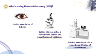
Why Scanning ElectronMicroscopy (SEM)?
Eye has a resolu
ti
on of
0.2 mm
Op
ti
cal microscope has a
resolu
ti
on of 200 nm and
magni
fi
ca
ti
on of 1000
ti
mes
SEM has a resolu
ti
on of 0.5
nm and magni
fi
ca
ti
on of
500,000
ti
mes
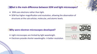
3.
What is themain di
ff
erence between SEM and light microscopes?
• SEM uses electrons rather than light.
• SEM has higher magni
fi
ca
ti
on and resolu
ti
on, allowing the observa
ti
on of
structures at the sub-cellular, molecular, and atomic levels.
Why were electron microscopes developed?
• Light microscopes are limited by light wavelength.
• Electrons provide shorter wavelengths → be
tt
er resolu
ti
on.
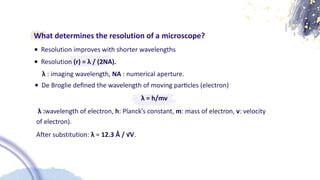
4.
What determines theresolution of a microscope?
• Resolution improves with shorter wavelengths
• Resolution (r) = λ / (2NA).
λ : imaging wavelength, NA : numerical aperture.
λ = h/mv
λ :wavelength of electron, h: Planck’s constant, m: mass of electron, v: velocity
of electron).
After substitution: λ ≈ 12.3 Å / √V.
• De Broglie de
fi
ned the wavelength of moving par
ti
cles (electron)
5.
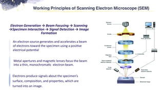
An electron sourcegenerates and accelerates a beam
of electrons toward the specimen using a posi
ti
ve
electrical poten
ti
al
Working Principles of Scanning Electron Microscope (SEM)
Metal apertures and magne
ti
c lenses focus the beam
into a thin, monochroma
ti
c electron beam.
Electrons produce signals about the specimen’s
surface, composi
ti
on, and proper
ti
es, which are
turned into an image.
Electron Generation → Beam Focusing → Scanning
→Specimen Interaction → Signal Detection → Image
Formation
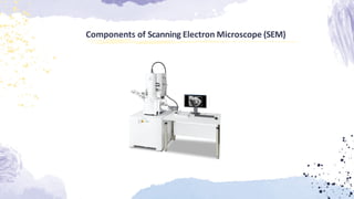
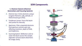
SEM Components
1. ElectronColumn (Electron
Generation and Focusing System):
A. Electron Gun: Emits electrons using a
tungsten filament, LaB₆ cathode, or
field emission gun (FEG).
B. Condenser Lenses: Focus the beam
and control its intensity.
C. Apertures: Filter unwanted electrons
final aperture controls spot size,
affecting resolution, depth of field,
and brightness.
D. Scanning System: Deflection coils to
raster the beam across the sample;
stigmator corrects beam distortions
for image clarity.
8.
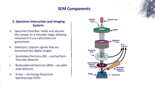
SEM Components
2. SpecimenInteraction and Imaging
System:
A. Specimen Chamber: Holds and secures
the sample on a movable stage, allowing
movement in x-y-z directions via
goniometer.
B. Detectors: Capture signals that are
converted into digital images:
i. Secondary Electrons (SE) – via Everhart–
Thornley detector.
ii. Backscattered Electrons (BSE) – via solid-
state detector.
iii. X-rays – via Energy Dispersive
Spectroscopy (EDS).
9.
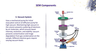
SEM Components
3. VacuumSystem:
Uses a mechanical pump for initial
evacuation and an oil diffusion pump for
high vacuum. Maintaining high vacuum in
the column prevents scattering of electrons
by air molecules, which ensures beam
intensity, resolution, and stability. vacuum
prevents contamination and image
degradation from gas condensation on the
sample. Different electron guns require
varying vacuum levels.
10.
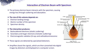
• The primaryelectron beam interacts with the specimen, causing
energy loss through sca
tt
ering and absorp
ti
on.
• The size of this volume depends on:
1. Electron landing energy
2. Atomic number of the specimen
3. Specimen density
• The interac
ti
on produces:
A. Backsca
tt
ered electrons (elas
ti
c sca
tt
ering)
B. Secondary and Auger electrons (inelas
ti
c sca
tt
ering)
C. Electromagne
ti
c radia
ti
on (X-rays and cathodoluminescence)
• These signals are detected by specialized detectors.
• Ampli
fi
ers boost the signals, which are then converted into digital
images by detectors and displayed on a computer screen.
Interac
ti
on of Electron Beam with Specimen
11.
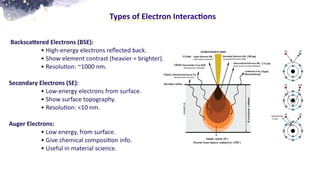
Backsca
tt
ered Electrons (BSE):
•High-energy electrons re
fl
ected back.
• Show element contrast (heavier = brighter).
• Resolu
ti
on: ~1000 nm.
Secondary Electrons (SE):
• Low-energy electrons from surface.
• Show surface topography.
• Resolu
ti
on: <10 nm.
Auger Electrons:
• Low energy, from surface.
• Give chemical composi
ti
on info.
• Useful in material science.
Types of Electron Interac
ti
ons
12.
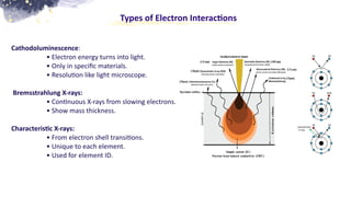
Cathodoluminescence:
• Electron energyturns into light.
• Only in speci
fi
c materials.
• Resolu
ti
on like light microscope.
Bremsstrahlung X-rays:
• Con
ti
nuous X-rays from slowing electrons.
• Show mass thickness.
Characteris
ti
c X-rays:
• From electron shell transi
ti
ons.
• Unique to each element.
• Used for element ID.
Types of Electron Interac
ti
ons
13.
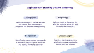
Composition
Identifies the elementsand compounds
in a material, impacting characteristics
like melting point and reactivity
Crystallography
Examines atomic arrangement,
which determines proper
ti
es like
conduc
ti
vity and strength
Applica
ti
ons of Scanning Electron Microscopy
Topography Morphology
Refers to par
ti
cle shape and size,
a
ff
ec
ti
ng material proper
ti
es such
as strength and duc
ti
lity.
Describes an object’s surface features
and texture, which in
fl
uence its
proper
ti
es like hardness and re
fl
ec
ti
vity
14.
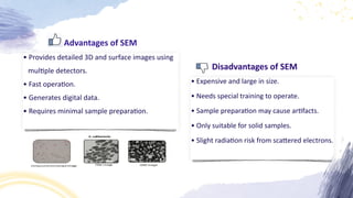
• Provides detailed3D and surface images using
mul
ti
ple detectors.
• Fast opera
ti
on.
• Generates digital data.
• Requires minimal sample prepara
ti
on.
Advantages of SEM
• Expensive and large in size.
• Needs special training to operate.
• Sample prepara
ti
on may cause ar
ti
facts.
• Only suitable for solid samples.
• Slight radia
ti
on risk from sca
tt
ered electrons.
Disadvantages of SEM
15.
Reference
Ch 8 :A Textbook on Fundamentals and Applications of Nanotechnology,
K. S. Subramanian, et al.


![SEM_Group_2_ppt[1]..pptxtttttttttttttttt](https://cdn.slidesharecdn.com/ss_thumbnails/semgroup2ppt1-250821082712-4dd54452-thumbnail.jpg?width=640&height=640&fit=bounds)


