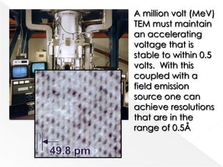
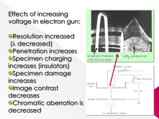
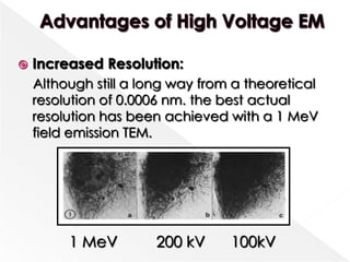
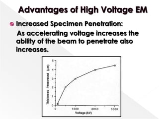
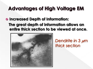
The greater the
accelerating
voltage the shorter
the
Therefore, a 50,000 volt (50 kV) electron has a
wavelength of 0.0055nm and a 1MeV electron has
a wavelength of 0.00123nm!
A million volt (MeV)
TEM must maintain
an accelerating
voltage that is
stable to within 0.5
volts. With this
coupled with a
field emission
source one can
achieve resolutions
that are in the
range of 0.5Å
The illumination system
Electron gun
Condenser
The image forming system
Objective lens
The projective system
Several projector lens
Aperture
Affect the image and diffraction
pattern
 High Voltage Source is same in principle as
in TEM (Heated filament)
 A Cockcroft Walton Rectifier-condenser
stack for voltage multiplication
 Feedback system for regulating the output
 Double feed-back system is used.
 Fast loop for dealing with ripple
 slow loop for drift
 Multi stage accelerator are used
 Maximum voltage per stage depends on
1. Design & finish of the electrodes
2. On that of containing tube
3. Degree of vacum
 Raising the voltage in steps of 25-50 kV at intervals of a
few minutes
 In U.S steel installation max. achievable voltage per
stage is 150 Kv
 In Japanese HVEM more stages (25) are used
 The injector gun is
supplied by a
transistorized power unit
house
 Large aluminium dome is
used
 It acts as corona shield
over the accelerator
column.
 Operating conditions of
the gun are controlled
by:
 Servo-motors driving
insulating rods
 Light beams
Effects of increasing
voltage in electron gun:
Resolution increased
( decreased)
Penetration increases
Specimen charging
increases (insulators)
Specimen damage
increases
Image contrast
decreases
Chromatic aberration is
decreased
In this column
 Electron beam is generated under vacuum,
focused to a small diameter & scanned
across the specimen by electromagnetic
lens
 Lower portion of the column is called
specimen chamber
 Japanese microscopes have more massive
columns, up to 50 cm in diameter.
 It provide adequate protection in all
operating conditions.
 Consists of two condenser lens
 1st is stronger & 2nd is weaker
 Minimum spot size is being less than 1mm
 An electromagnetic double deflection system is
used mounted b/w 2nd condenser and the
objective
 Allows a controlled tilt & shift of illuminating for
alignment and for dark field imaging
 It consists of two projectors
 1st is stronger & 2nd is weaker
 The overall magnification range in normal
operations
2000× to 140000 ×
 As the range of 750-1000 kv electrons is
about 30 times that at 100 kv the viewing
screen has to be modified.
 Thicken the fluorescent layer leads to
blurring of image details.
 Best solution is to mount phosphor on
sheet of plastic
 Optimum thickness is a compromise b/w
image brightness & resolution at high
temperature
 Increased Resolution:
Although still a long way from a theoretical
resolution of 0.0006 nm. the best actual
resolution has been achieved with a 1 MeV
field emission TEM.
1 MeV 200 kV 100kV
 Increased Specimen Penetration:
As accelerating voltage increases the
ability of the beam to penetrate also
increases.
 Increased Depth of Information:
The great depth of information allows an
entire thick section to be viewed at once.
Dendrite in 3 m
thick section
 Reduced Beam Damage:
The increased speed of the electrons
actually decreases the likelihood of an
inelastic collision.

Presentation high voltage electron microscope

  • 4.
    The greater the accelerating voltagethe shorter the Therefore, a 50,000 volt (50 kV) electron has a wavelength of 0.0055nm and a 1MeV electron has a wavelength of 0.00123nm!
  • 5.
    A million volt(MeV) TEM must maintain an accelerating voltage that is stable to within 0.5 volts. With this coupled with a field emission source one can achieve resolutions that are in the range of 0.5Å
  • 6.
    The illumination system Electrongun Condenser The image forming system Objective lens The projective system Several projector lens Aperture Affect the image and diffraction pattern
  • 7.
     High VoltageSource is same in principle as in TEM (Heated filament)  A Cockcroft Walton Rectifier-condenser stack for voltage multiplication  Feedback system for regulating the output  Double feed-back system is used.  Fast loop for dealing with ripple  slow loop for drift
  • 8.
     Multi stageaccelerator are used  Maximum voltage per stage depends on 1. Design & finish of the electrodes 2. On that of containing tube 3. Degree of vacum  Raising the voltage in steps of 25-50 kV at intervals of a few minutes  In U.S steel installation max. achievable voltage per stage is 150 Kv  In Japanese HVEM more stages (25) are used
  • 9.
     The injectorgun is supplied by a transistorized power unit house  Large aluminium dome is used  It acts as corona shield over the accelerator column.  Operating conditions of the gun are controlled by:  Servo-motors driving insulating rods  Light beams
  • 10.
    Effects of increasing voltagein electron gun: Resolution increased ( decreased) Penetration increases Specimen charging increases (insulators) Specimen damage increases Image contrast decreases Chromatic aberration is decreased
  • 11.
    In this column Electron beam is generated under vacuum, focused to a small diameter & scanned across the specimen by electromagnetic lens  Lower portion of the column is called specimen chamber  Japanese microscopes have more massive columns, up to 50 cm in diameter.  It provide adequate protection in all operating conditions.
  • 13.
     Consists oftwo condenser lens  1st is stronger & 2nd is weaker  Minimum spot size is being less than 1mm  An electromagnetic double deflection system is used mounted b/w 2nd condenser and the objective  Allows a controlled tilt & shift of illuminating for alignment and for dark field imaging
  • 14.
     It consistsof two projectors  1st is stronger & 2nd is weaker  The overall magnification range in normal operations 2000× to 140000 ×
  • 15.
     As therange of 750-1000 kv electrons is about 30 times that at 100 kv the viewing screen has to be modified.  Thicken the fluorescent layer leads to blurring of image details.  Best solution is to mount phosphor on sheet of plastic  Optimum thickness is a compromise b/w image brightness & resolution at high temperature
  • 18.
     Increased Resolution: Althoughstill a long way from a theoretical resolution of 0.0006 nm. the best actual resolution has been achieved with a 1 MeV field emission TEM. 1 MeV 200 kV 100kV
  • 19.
     Increased SpecimenPenetration: As accelerating voltage increases the ability of the beam to penetrate also increases.
  • 20.
     Increased Depthof Information: The great depth of information allows an entire thick section to be viewed at once. Dendrite in 3 m thick section
  • 21.
     Reduced BeamDamage: The increased speed of the electrons actually decreases the likelihood of an inelastic collision.