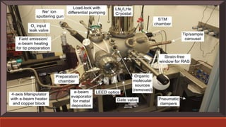
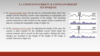
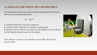
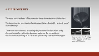
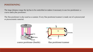
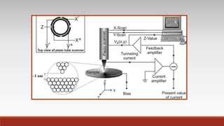
The document discusses the scanning tunneling microscope (STM), its invention in 1981 by Gerd Binning and Heinrich Rohrer, and its significance in imaging conductive surfaces at atomic resolution. It explains the basic components of STM, the tunneling effect, and the principles behind its operation, along with its advantages and disadvantages compared to other microscopy methods. The document also highlights factors affecting the resolution and the piezoelectric effect essential for STM functionality.