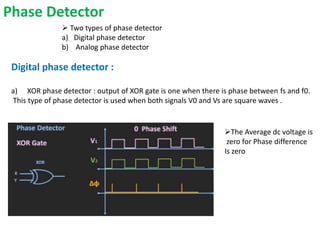
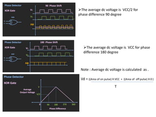
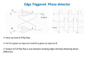
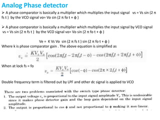
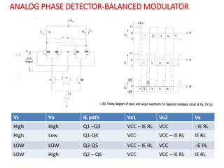
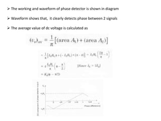
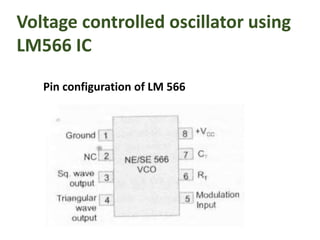
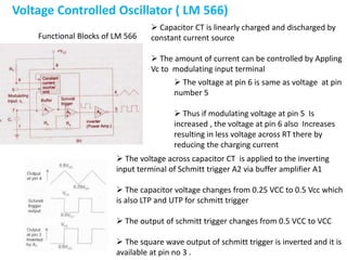
PHASE LOCKED LOOP (PLL)
Introduction
 Phase locked loop is a circuit that produces output signal which is synchronized with input
Signal in terms of frequency and phase .  The Basic block of PLL is
a) Phase Detector
b) Low pass filter
c) Error Amplifier
d) Voltage controlled Oscillator
VCO is a free running multi-vibrator which
operates at centre frequency fo .
 Phase Detector: The input signal Vs with an input frequency fs is passed through a phase
detector. A phase detector basically a comparator which compares the input frequency fs with
the feedback frequency fo which is output of VCO .
 Phase Detector is a multiplier circuit that produces sum and difference frequency
components (fs + fo) and (fs - fo) at its output .
 Low pass filter : High frequency component (fs + fo) is removed by low pass filter and
difference frequency component (fs – fo) is amplified by error amplifier and this control signal
Vc is applied to voltage controlled oscillator (VCO) .
 The signal Vc shifts the VCO frequency in direction to reduce frequency difference between
fs and fo . Once this operation starts , we say signal is in capture range .
 VCO continues to change in frequency till its output frequency is exactly same as input
frequency
 At this point PLL circuit is said to be locked .
 Once locked, output frequency of VCO fo is exactly equal to fs .
Thus PLL operates in 3 phases . A) Free running stage
B) Capture stage
C) Locked or tracking stage.
Lock in range : Once PLL is locked, it can track frequency changes in incoming signal.
The range of frequencies over which PLL can maintain lock with its incoming input signal is
called as lock in range . It is usually expressed as percentage change of fo.
Capture Range : The range of frequencies over which PLL can acquire lock with an
input signal is called as capture range . It is also expressed in percentage fo.
Pull in time : The total time taken by PLL to acquire lock is called pull in time
Phase Detector
 Two types of phase detector
a) Digital phase detector
b) Analog phase detector
Digital phase detector :
a) XOR phase detector : output of XOR gate is one when there is phase between fs and f0.
This type of phase detector is used when both signals V0 and Vs are square waves .
The Average dc voltage is
zero for Phase difference
Is zero
The average dc voltage is VCC/2 for
phase difference 90 degree
The average dc voltage is VCC for phase
difference 180 degree
Note : Average dc voltage is calculated as .
Vd = ((Area of on pulse) X VCC + ((Area of off pulse) X 0 )
T
Edge Triggered Phase detector
 Here we have S-R flip flop .
 For fs is given as input to S and fo is given as input to R.
 Output of S-R flip-flop is one between leading edges thereby detecting phase
difference .
Analog Phase detector
 A phase comparator is basically a multiplier which multiplies the input signal vs = Vs sin (2 π
fs t ) by the VCO signal vo= Vo sin (2 π fo t + φ )
 A phase comparator is basically a multiplier which multiplies the input signal by VCO signal
vs = Vs sin (2 π fs t ) by the VCO signal vo= Vo sin (2 π fo t + φ )
Ve = K Vs Vo sin (2 π fs t ) sin (2 π fo t + φ )
Where k is phase comparator gain . The above equation is simplified as
When at lock fs = fo
Double frequency term is filtered out by LPF and other dc signal is applied to VCO
ANALOG PHASE DETECTOR-BALANCED MODULATOR
Vs Vo IE path Ve1 Ve2 Ve
High High Q1 –Q3 VCC – IE RL VCC - IE RL
High Low Q1-Q4 VCC VCC – IE RL IE RL
LOW LOW Q2-Q5 VCC – IE RL VCC -IE RL
LOW High Q2 – Q6 VCC VCC – IE RL IE RL
 The working and waveform of phase detector is shown in diagram
 Waveform shows that, it clearly detects phase between 2 signals
 The average value of dc voltage is calculated as
Voltage controlled oscillator using
LM566 IC
Pin configuration of LM 566
Voltage Controlled Oscillator ( LM 566)
Functional Blocks of LM 566
 Capacitor CT is linearly charged and discharged by
constant current source
 The amount of current can be controlled by Appling
Vc to modulating input terminal
 The voltage at pin 6 is same as voltage at pin
number 5
 Thus if modulating voltage at pin 5 Is
increased , the voltage at pin 6 also Increases
resulting in less voltage across RT there by
reducing the charging current
 The voltage across capacitor CT is applied to the inverting
input terminal of Schmitt trigger A2 via buffer amplifier A1
 The capacitor voltage changes from 0.25 VCC to 0.5 Vcc which
is also LTP and UTP for schmitt trigger
 The output of schmitt trigger changes from 0.5 VCC to VCC
 The square wave output of schmitt trigger is inverted and it is
available at pin no 3 .
Output frequency of VCO :
 As capacitor voltage changes from 0.25 VCC to 0.5 VCC . Thus change in voltage is 0.25 VCC
 Capacitor voltage is given by
Substituting value CT RT from (2)

Phase locked loop

  • 1.
  • 2.
    Introduction  Phase lockedloop is a circuit that produces output signal which is synchronized with input Signal in terms of frequency and phase .  The Basic block of PLL is a) Phase Detector b) Low pass filter c) Error Amplifier d) Voltage controlled Oscillator VCO is a free running multi-vibrator which operates at centre frequency fo .  Phase Detector: The input signal Vs with an input frequency fs is passed through a phase detector. A phase detector basically a comparator which compares the input frequency fs with the feedback frequency fo which is output of VCO .  Phase Detector is a multiplier circuit that produces sum and difference frequency components (fs + fo) and (fs - fo) at its output .  Low pass filter : High frequency component (fs + fo) is removed by low pass filter and difference frequency component (fs – fo) is amplified by error amplifier and this control signal Vc is applied to voltage controlled oscillator (VCO) .
  • 3.
     The signalVc shifts the VCO frequency in direction to reduce frequency difference between fs and fo . Once this operation starts , we say signal is in capture range .  VCO continues to change in frequency till its output frequency is exactly same as input frequency  At this point PLL circuit is said to be locked .  Once locked, output frequency of VCO fo is exactly equal to fs . Thus PLL operates in 3 phases . A) Free running stage B) Capture stage C) Locked or tracking stage.
  • 4.
    Lock in range: Once PLL is locked, it can track frequency changes in incoming signal. The range of frequencies over which PLL can maintain lock with its incoming input signal is called as lock in range . It is usually expressed as percentage change of fo. Capture Range : The range of frequencies over which PLL can acquire lock with an input signal is called as capture range . It is also expressed in percentage fo. Pull in time : The total time taken by PLL to acquire lock is called pull in time
  • 5.
    Phase Detector  Twotypes of phase detector a) Digital phase detector b) Analog phase detector Digital phase detector : a) XOR phase detector : output of XOR gate is one when there is phase between fs and f0. This type of phase detector is used when both signals V0 and Vs are square waves . The Average dc voltage is zero for Phase difference Is zero
  • 6.
    The average dcvoltage is VCC/2 for phase difference 90 degree The average dc voltage is VCC for phase difference 180 degree Note : Average dc voltage is calculated as . Vd = ((Area of on pulse) X VCC + ((Area of off pulse) X 0 ) T
  • 7.
    Edge Triggered Phasedetector  Here we have S-R flip flop .  For fs is given as input to S and fo is given as input to R.  Output of S-R flip-flop is one between leading edges thereby detecting phase difference .
  • 8.
    Analog Phase detector A phase comparator is basically a multiplier which multiplies the input signal vs = Vs sin (2 π fs t ) by the VCO signal vo= Vo sin (2 π fo t + φ )  A phase comparator is basically a multiplier which multiplies the input signal by VCO signal vs = Vs sin (2 π fs t ) by the VCO signal vo= Vo sin (2 π fo t + φ ) Ve = K Vs Vo sin (2 π fs t ) sin (2 π fo t + φ ) Where k is phase comparator gain . The above equation is simplified as When at lock fs = fo Double frequency term is filtered out by LPF and other dc signal is applied to VCO
  • 9.
    ANALOG PHASE DETECTOR-BALANCEDMODULATOR Vs Vo IE path Ve1 Ve2 Ve High High Q1 –Q3 VCC – IE RL VCC - IE RL High Low Q1-Q4 VCC VCC – IE RL IE RL LOW LOW Q2-Q5 VCC – IE RL VCC -IE RL LOW High Q2 – Q6 VCC VCC – IE RL IE RL
  • 10.
     The workingand waveform of phase detector is shown in diagram  Waveform shows that, it clearly detects phase between 2 signals  The average value of dc voltage is calculated as
  • 11.
    Voltage controlled oscillatorusing LM566 IC Pin configuration of LM 566
  • 12.
    Voltage Controlled Oscillator( LM 566) Functional Blocks of LM 566  Capacitor CT is linearly charged and discharged by constant current source  The amount of current can be controlled by Appling Vc to modulating input terminal  The voltage at pin 6 is same as voltage at pin number 5  Thus if modulating voltage at pin 5 Is increased , the voltage at pin 6 also Increases resulting in less voltage across RT there by reducing the charging current  The voltage across capacitor CT is applied to the inverting input terminal of Schmitt trigger A2 via buffer amplifier A1  The capacitor voltage changes from 0.25 VCC to 0.5 Vcc which is also LTP and UTP for schmitt trigger  The output of schmitt trigger changes from 0.5 VCC to VCC  The square wave output of schmitt trigger is inverted and it is available at pin no 3 .
  • 13.
    Output frequency ofVCO :  As capacitor voltage changes from 0.25 VCC to 0.5 VCC . Thus change in voltage is 0.25 VCC  Capacitor voltage is given by
  • 14.