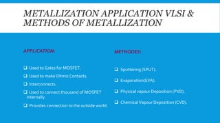
This document provides an overview of metallization for integrated circuits. It discusses the requirements and purposes of metallization, including interconnecting thousands of devices on chips. Two common metallization methods described are vacuum evaporation and sputter deposition. Vacuum evaporation locally heats a material source to vaporize and deposit the metal film, while sputter deposition uses ion momentum from a plasma to eject atoms from a target onto the substrate. The document outlines the apparatus and processes for each technique.


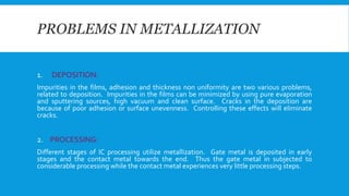


![Thin_Film_Technology_introduction[1]](https://cdn.slidesharecdn.com/ss_thumbnails/1b4496c8-2102-411b-8465-a3dd3f398327-150205034538-conversion-gate02-thumbnail.jpg?width=640&height=640&fit=bounds)


