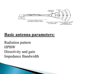
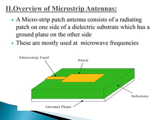
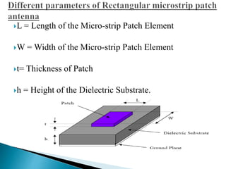
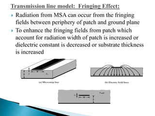
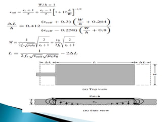
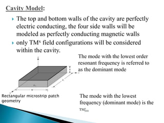
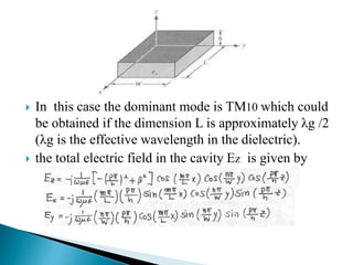
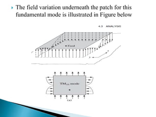
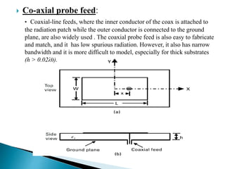
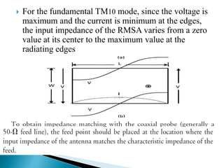
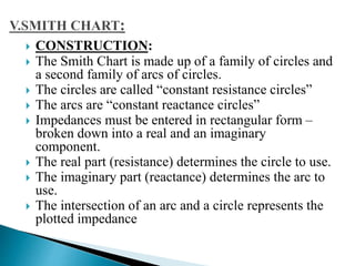
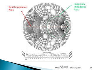
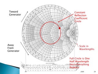
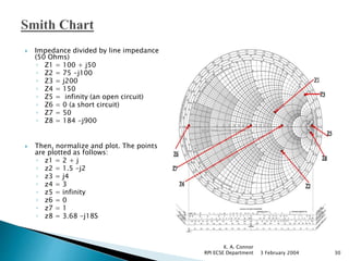
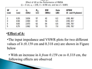
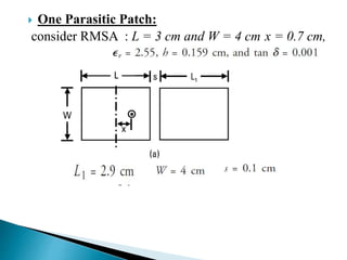
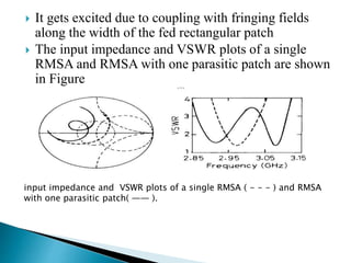
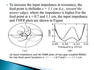
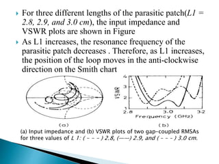
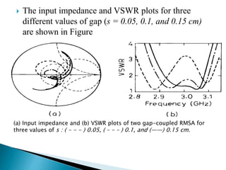
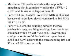
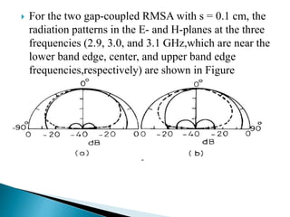
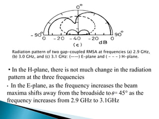
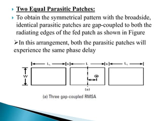
K.SREELAKSHMI
DEPT OF ECE
PRESENTED BY
GVPCEW
OUTLINE:
 INTRODUCTION
 OVERVIEW OF MICROSTRIP ANTENNAS
 METHODS OF ANALYSIS
 FEEDING TECHNIQUES
 SMITH CHART
 PARAMETRIC STUDY OF RMSAS
 PLANAR MULTIRESONATOR BROADBAND MSAs
 Antenna is defined as “a usually metallic device (as a
rod or wire) for radiating or receiving radio waves.”
But as for IEEE standard definitions of terms for
antenna or aerial as “a mean for radiating or receiving
radio waves.”
 Antenna is defined as region of transition between
guided wave and free space wave
Basic antenna parameters:
Radiation pattern
HPBW
Directivity and gain
Impedance Bandwidth
 A Micro-strip patch antenna consists of a radiating
patch on one side of a dielectric substrate which has a
ground plane on the other side
 These are mostly used at microwave frequencies
L = Length of the Micro-strip Patch Element
W = Width of the Micro-strip Patch Element
t= Thickness of Patch
h = Height of the Dielectric Substrate.
 t<< λ0, where λ0 is the free-space wavelength
 h << λ0, usually 0.003λ0 ≤ h ≤ 0.05λ0
 λ0/3 < L < λ0/2
 .
Equivalent resonant parallel RLC circuit:
• for good antenna performance are thick substrates whose
dielectric constant is in the lower end of the range because
they provide better efficiency, larger bandwidth, but at the
expense of larger element size
• Thin substrates with higher dielectric constants are
desirable for microwave circuitry, and lead to smaller
element sizes , however because of their greater losses,
they are less efficient and have relatively smaller
bandwidths
• Compromise has to be reached between good antenna
performance and circuit design.
Definition of BW:
 The VSWR or impedance BW of the MSA is defined as the
frequency range over which it is matched with that of the feed
line within specified limits
 The BW of the MSA is inversely proportional to its quality
factor Q and is given by
• The expressions for approximately calculating the %BW of the
RMSA in terms of patch dimensions and substrate parameters is
given by
 Transmission line model:
This model represents Rectangular microstrip patch
antenna by two slots seperated by a low impedance
transmission line of length L
 Cavity model:
This model represents Rectangular microstrip patch
antenna as an array of two radiating slots each of width W and
height h seperated by distance L
 Radiation from MSA can occur from the fringing
fields between periphery of patch and ground plane
 To enhance the fringing fields from patch which
account for radiation width of patch is increased or
dielectric constant is decreased or substrate thickness
is increased
 The top and bottom walls of the cavity are perfectly
electric conducting, the four side walls will be
modeled as perfectly conducting magnetic walls
 only TMx field configurations will be considered
within the cavity.
The mode with the lowest order
resonant frequency is referred to
as the dominant mode
The mode with the lowest
frequency (dominant mode) is the
Rectangular microstrip patch
geometry
 In this case the dominant mode is TM10 which could
be obtained if the dimension L is approximately λg /2
(λg is the effective wavelength in the dielectric).
 the total electric field in the cavity Ez is given by
 The field variation underneath the patch for this
fundamental mode is illustrated in Figure below
 The left- and right-edge fringing fields do not
contribute much to far fields due to their oscillatory
behavior and, hence, cancel each other in the far
field. The top- and bottom-edge fringing fields are
the primary contributors to the far-field radiation of a
patch.
 The far zone electric fields radiated by patch antenna
is given by
•A secondary higher order mode that does contribute significantly to
the cross-polarization radiation is the TM02 mode. This mode, shown
in Figure below, has the left and right edges contributing to the far-
field radiation but with lower magnitude than the TM10 mode.
FEEDING METHODS
CONTACTING
Microstripline Co-ax probe
NON CONTACTING
APERTURE
COUPLING
PROXIMITY
COUPLING
 Co-axial probe feed:
• Coaxial-line feeds, where the inner conductor of the coax is attached to
the radiation patch while the outer conductor is connected to the ground
plane, are also widely used . The coaxial probe feed is also easy to fabricate
and match, and it has low spurious radiation. However, it also has narrow
bandwidth and it is more difficult to model, especially for thick substrates
(h > 0.02λ0).
 For the fundamental TM10 mode, since the voltage is
maximum and the current is minimum at the edges,
the input impedance of the RMSA varies from a zero
value at its center to the maximum value at the
radiating edges
Advantages:
Disadvantages:
1.Co-axial feeding of array requires large no of solder
joints which makes fabrication difficult
2.To increase the bandwidth of patch antenna thicker
substrate is used and therefore requires longer probe. This gives
rise to increase in spurious radiation from the probe, increased
surface wave power and increased probe inductance
 CONSTRUCTION:
 The Smith Chart is made up of a family of circles and
a second family of arcs of circles.
 The circles are called “constant resistance circles”
 The arcs are “constant reactance circles”
 Impedances must be entered in rectangular form –
broken down into a real and an imaginary
component.
 The real part (resistance) determines the circle to use.
 The imaginary part (reactance) determines the arc to
use.
 The intersection of an arc and a circle represents the
plotted impedance
It is a polar plot of the complex reflection coefficient
 = (ZR – Z0) / (ZR + Z0)
For Open circuited line, ZR =  , Hence
= (1-Z0/ZR) / (1+ZR/Z0)=1
For Short circuited line, ZR=0, Hence
 = -Z0/Z0 = -1
1+  
1-  
S = s -1
s +1
 =
0,
• A circle is drawn that represents the reflection
coefficient or SWR. The center of the circle is the center
of the chart.
3 February 2004
K. A. Connor
RPI ECSE Department 28
Real Impedance
Axis
Imaginary
Impedance
Axis
3 February 2004
K. A. Connor
RPI ECSE Department 29
Toward
Generator
Away
From
Generator
Constant
Reflection
Coefficient
Circle
Scale in
Wavelengths
Full Circle is One
Half Wavelength
Since Everything
Repeats
 Impedance divided by line impedance
(50 Ohms)
◦ Z1 = 100 + j50
◦ Z2 = 75 -j100
◦ Z3 = j200
◦ Z4 = 150
◦ Z5 = infinity (an open circuit)
◦ Z6 = 0 (a short circuit)
◦ Z7 = 50
◦ Z8 = 184 -j900
 Then, normalize and plot. The points
are plotted as follows:
◦ z1 = 2 + j
◦ z2 = 1.5 -j2
◦ z3 = j4
◦ z4 = 3
◦ z5 = infinity
◦ z6 = 0
◦ z7 = 1
◦ z8 = 3.68 -j18S
3 February 2004
K. A. Connor
RPI ECSE Department 30
 consider RMSA : L = 3 cm and W = 4 cm
probe : diameter = 0.12 cm
 The size of the ground plane is considered to be
infinite unless finite ground plane size is specified.
 Effect of Feed-Point Location:
 For three different feed-point locations from the center
of the patch (i.e. x = 0.55, 0.6, and 0.65 cm), the
variations of the input impedance Zin and VSWR with
frequency are shown in figure below
(a) Input impedance and (b) VSWR plots of the RMSA for three different values
of x , ( - - - ) 0.55, ( – - – ) 0.60, and (——) 0.65 cm
 With an increase in frequency, the input impedance
moves in the clockwise direction in the Smith chart
 As x increases from 0.55 cm to 0.65 cm (i.e., the feed
point is shifted toward the edge), the input impeda
nce loci shifts in the right direction on the Smith chart
implying that the impedance is increasing
 Resonance frequency of the RMSA obtained using
IE3D is 2.974 GHz. The resonance frequency
calculated using is 3.003 GHz
 A perfect match with a 50ohm feed line is obtained
for x = 0.59 cm, which gives a BW of 60 MHz for
VSWR<=2 ; however, it is not the maximum BW. A
larger BW of 64 MHz for x = 0.65 cm is obtained for
which Zin at the resonance is 62 ohms
x = 0.65 cm is shown in Figure below
•Effect of W:
•The width W of the RMSA has significant effect on the
input impedance, BW, and gain of the antenna. For four
different values of W (2, 3, 4, and 5 cm), the input
impedance and VSWR plots for x = 0.65 cm are given in
Figure
•Effect of h:
•The input impedance and VSWR plots for two different
values of h (0.159 cm and 0.318 cm) are shown in Figure
below
• With an increase in h from 0.159 cm to 0.318 cm, the
following effects are observed
(a) Input impedance and (b) VSWR plots of the RMSA for
two different values of h: ( - - - ) 0.159 and (——) 0.318 cm.
•The loss due to surface waves can be neglected when h satisfies the following
criterion
•Effect of Probe Diameter:
 An RMSA can be fed with different types of
connectors, such as SMA, TNC, and N type
connectors, depending upon the application.
 The diameters of these connectors are different, and
as the probe diameter d increases, the probe
inductance decreases for the same substrate thickness
 With an increase in the probe diameter, the probe
inductance decreases and hence the impedance plot
moves in the anticlockwise direction, and resonance
frequency increases slightly
 Effect of Finite Ground Plane:
 when the size of the ground plane is greater than the
patch dimensions by approximately six times the
substrate thickness all around the periphery, the
results are similar to that of the infinite ground plane
 Input impedance and VSWR plots for infinite and
finite ground planes (length = 5 cm and width = 6cm)
are shown in Figure below
 For this finite ground plane, the resonance frequency
of the RMSA is almost the same but the input
impedance is slightly higher than that of the infinite
ground plane
 For the finite ground plane, the back lobes are present
, where as for the infinite ground plane, there are no
back lobes in the radiation pattern as shown in Figure
Mechanism of Parasitic Coupling for Broad BW:
•A patch placed close to the fed patch gets excited
through the coupling between the two patches. Such a
patch is known as a parasitic patch. If the resonance
frequencies f 1 and f 2 of these two patches are close to
each other, then broad BW is obtained
 If the BW is narrow for the individual patch, then the
difference between f 1 and f 2 should be small
 If the BW of the individual patch is large, then the
difference in the two frequencies should be large to
yield an overall wide BW
Radiating-Edge Gap-Coupled RMSAs:
 Either one or two parasitic rectangular patches can be
placed along one or both of the radiating edges of the
fed rectangular patch with a small gap between them
 To adjust the parasitic patch size, the distance
between the driven and the parasitic elements and the
position of the feeding point, the iterative process is
used
 The process can be summarized as follows
 One Parasitic Patch:
consider RMSA : L = 3 cm and W = 4 cm x = 0.7 cm,
 It gets excited due to coupling with fringing fields
along the width of the fed rectangular patch
 The input impedance and VSWR plots of a single
RMSA and RMSA with one parasitic patch are shown
in Figure
input impedance and VSWR plots of a single RMSA ( - - - ) and RMSA
with one parasitic patch( —— ).
 To increase the input impedance at resonance, the
feed point is shiftedto x = 1.1 cm (i.e., toward the
nearer edge), where the impedance is higher.For the
feed point at x = 0.7 and 1.1 cm, the input impedance
and VSWR plots are shown in Figure
(a) Input impedance and (b) VSWR plots of two gap-coupled RMSAs
for two feed-point locations x : ( - - - ) 0.7 and ( —— ) 1.1 cm.
 For three different lengths of the parasitic patch(L1 =
2.8, 2.9, and 3.0 cm), the input impedance and
VSWR plots are shown in Figure
 As L1 increases, the resonance frequency of the
parasitic patch decreases . Therefore, as L1 increases,
the position of the loop moves in the anti-clockwise
direction on the Smith chart
(a) Input impedance and (b) VSWR plots of two gap-coupled RMSAs
for three values of L 1: ( - - - ) 2.8, (——) 2.9, and ( – - – ) 3.0 cm.
 The input impedance and VSWR plots for three
different values of gap (s = 0.05, 0.1, and 0.15 cm)
are shown in Figure
(a) Input impedance and (b) VSWR plots of two gap-coupled RMSA for
three values of s : ( - - - ) 0.05, ( – - – ) 0.1, and (——) 0.15 cm.
 Maximum BW is obtained when the loop in the
impedance plot is completely inside the VSWR = 2
circle and its size is as large as possible
 For s = 0.1 cm, broader BW of 207 MHz is obtained
because of larger loop size as compared to 161 MHz
for s = 0.15 cm.
 For s = 0.05 cm, the coupling between the two
patches is strong, resulting in a large loop that is not
contained within VSWR = 2 circle. However, this
configuration is useful for dual-band operation at
2.884 and 3.093 GHz with the corresponding BWs of
97 and 47 MHz, respectively
 For the two gap-coupled RMSA with s = 0.1 cm, the
radiation patterns in the E- and H-planes at the three
frequencies (2.9, 3.0, and 3.1 GHz,which are near the
lower band edge, center, and upper band edge
frequencies,respectively) are shown in Figure
Radiation pattern of two gap-coupled RMSA at frequencies (a) 2.9 GHz,
(b) 3.0 GHz, and (c) 3.1 GHz: (——) E-plane and ( - - - ) H-plane.
• In the H-plane, there is not much change in the radiation
pattern at the three frequencies
• In the E-plane, as the frequency increases the beam
maxima shifts away from the broadside to = 45° as the
frequency increases from 2.9 GHz to 3.1GHz
 Two Equal Parasitic Patches:
 To obtain the symmetrical pattern with the broadside,
identical parasitic patches are gap-coupled to both the
radiating edges of the fed patch as shown in Figure
In this arrangement, both the parasitic patches will
experience the same phase delay
 The input impedance and VSWR plots for the three-
radiating-edge gap-coupled RMSA is shown in Figure
 The loop size is large compared to the two gap-coupled
RMSA, because two coupled patches are resonant at the
same frequency and hence the coupling is greater
 The loop size is reduced by increasing the gap between
the fed and the parasitic patches
 The input impedance and VSWR plots for two
different values of s (0.15 cm and 0.2 cm) are also
shown in Figure . The loop in the impedance plot for
s = 0.15 and 0.2 cm is completely inside the VSWR =
2 circle, yielding BWs of 209 MHz and 171 MHz,
respectively. The BW for s = 0.15 cm is larger than
that for s = 0.20 cm because of the larger loop size.
(b) input impedance and (c) VSWR plotsfor three values of s : ( – - – )
0.1, ( - - - ) 0.15, and (——) 0.2 cm
The radiation patterns in the E- and H-planes near the two-
band edge frequencies (2.89 GHz and 3.09 GHz) for s =
0.15 cm are shown in Figure
Radiation pattern of three gap-coupled RMSA at frequencies (a) 2.89
and (b) 3.09 GHz: (——) E-plane and ( - - - ) H-plane.
•As the frequency increases, the sidelobes begin to appear
due to the large overall length of the antenna in this plane
• The HPBW in the E-plane is smaller than that of the two
gap-coupled configurations due to increase in the aperture
area
 By adding two parasitic patches the gain of the antenna
increases from 6.7 dB to 9.4 dB, and the BW increases from
65 MHz to 209 MHz at the expense of increase in the size of
the antenna
 The BW of the three gap-coupled RMSA can be increased by
increasing h, as in the case of single RMSA
 If the BW of an individual patch is large, then the difference
between the two patch dimensions should also be large to
obtain broader BW
 when h is increased from 0.159 cm to 0.318 cm, and if the
parasitic patch of length L1 = 2.9 cm is placed along both the
radiating edges of the RMSA, then the BW will not be
optimum
 The coupling between the fed and parasitic patches depends
upon the s /h ratio and not on the s value alone, so the gap has
been increased from 0.15 cm to 0.3 cm for three gap-coupled
RMSA
 For the feed at x = 1.4 cm, the input impedance plot
is shown in Figure
 The length L1 of the parasitic patch is decreased, so
the loop will be formed in the higher frequency
region and therefore moves in the clockwise direction
 For L1 = 2.75 cm, the input impedance and VSWR
plots are also shown in Figure
(a) Input impedance and (b) VSWR plots of three gap-coupled RMSA
with h = 0.318 cm for two values of L 1: ( - - - ) 2.9 cm and ( —— )
2.75 cm.
 The loop is completely inside the VSWR = 2 circle,
yielding a BW of 335 MHz (11.3%).
 The gain of the antenna at 3 GHz is 9.2 dB.The gain
is slightly decreased as compared to that of the
antenna with h = 0.159 cm due to an increase in the
surface waves

Basics of Patch antenna

  • 1.
  • 2.
    OUTLINE:  INTRODUCTION  OVERVIEWOF MICROSTRIP ANTENNAS  METHODS OF ANALYSIS  FEEDING TECHNIQUES  SMITH CHART  PARAMETRIC STUDY OF RMSAS  PLANAR MULTIRESONATOR BROADBAND MSAs
  • 3.
     Antenna isdefined as “a usually metallic device (as a rod or wire) for radiating or receiving radio waves.” But as for IEEE standard definitions of terms for antenna or aerial as “a mean for radiating or receiving radio waves.”  Antenna is defined as region of transition between guided wave and free space wave
  • 4.
    Basic antenna parameters: Radiationpattern HPBW Directivity and gain Impedance Bandwidth
  • 5.
     A Micro-strippatch antenna consists of a radiating patch on one side of a dielectric substrate which has a ground plane on the other side  These are mostly used at microwave frequencies
  • 6.
    L = Lengthof the Micro-strip Patch Element W = Width of the Micro-strip Patch Element t= Thickness of Patch h = Height of the Dielectric Substrate.
  • 7.
     t<< λ0,where λ0 is the free-space wavelength  h << λ0, usually 0.003λ0 ≤ h ≤ 0.05λ0  λ0/3 < L < λ0/2  . Equivalent resonant parallel RLC circuit:
  • 8.
    • for goodantenna performance are thick substrates whose dielectric constant is in the lower end of the range because they provide better efficiency, larger bandwidth, but at the expense of larger element size • Thin substrates with higher dielectric constants are desirable for microwave circuitry, and lead to smaller element sizes , however because of their greater losses, they are less efficient and have relatively smaller bandwidths • Compromise has to be reached between good antenna performance and circuit design.
  • 9.
    Definition of BW: The VSWR or impedance BW of the MSA is defined as the frequency range over which it is matched with that of the feed line within specified limits  The BW of the MSA is inversely proportional to its quality factor Q and is given by • The expressions for approximately calculating the %BW of the RMSA in terms of patch dimensions and substrate parameters is given by
  • 10.
     Transmission linemodel: This model represents Rectangular microstrip patch antenna by two slots seperated by a low impedance transmission line of length L  Cavity model: This model represents Rectangular microstrip patch antenna as an array of two radiating slots each of width W and height h seperated by distance L
  • 11.
     Radiation fromMSA can occur from the fringing fields between periphery of patch and ground plane  To enhance the fringing fields from patch which account for radiation width of patch is increased or dielectric constant is decreased or substrate thickness is increased
  • 13.
     The topand bottom walls of the cavity are perfectly electric conducting, the four side walls will be modeled as perfectly conducting magnetic walls  only TMx field configurations will be considered within the cavity. The mode with the lowest order resonant frequency is referred to as the dominant mode The mode with the lowest frequency (dominant mode) is the Rectangular microstrip patch geometry
  • 14.
     In thiscase the dominant mode is TM10 which could be obtained if the dimension L is approximately λg /2 (λg is the effective wavelength in the dielectric).  the total electric field in the cavity Ez is given by
  • 15.
     The fieldvariation underneath the patch for this fundamental mode is illustrated in Figure below
  • 16.
     The left-and right-edge fringing fields do not contribute much to far fields due to their oscillatory behavior and, hence, cancel each other in the far field. The top- and bottom-edge fringing fields are the primary contributors to the far-field radiation of a patch.  The far zone electric fields radiated by patch antenna is given by
  • 18.
    •A secondary higherorder mode that does contribute significantly to the cross-polarization radiation is the TM02 mode. This mode, shown in Figure below, has the left and right edges contributing to the far- field radiation but with lower magnitude than the TM10 mode.
  • 19.
    FEEDING METHODS CONTACTING Microstripline Co-axprobe NON CONTACTING APERTURE COUPLING PROXIMITY COUPLING
  • 20.
     Co-axial probefeed: • Coaxial-line feeds, where the inner conductor of the coax is attached to the radiation patch while the outer conductor is connected to the ground plane, are also widely used . The coaxial probe feed is also easy to fabricate and match, and it has low spurious radiation. However, it also has narrow bandwidth and it is more difficult to model, especially for thick substrates (h > 0.02λ0).
  • 21.
     For thefundamental TM10 mode, since the voltage is maximum and the current is minimum at the edges, the input impedance of the RMSA varies from a zero value at its center to the maximum value at the radiating edges
  • 23.
    Advantages: Disadvantages: 1.Co-axial feeding ofarray requires large no of solder joints which makes fabrication difficult 2.To increase the bandwidth of patch antenna thicker substrate is used and therefore requires longer probe. This gives rise to increase in spurious radiation from the probe, increased surface wave power and increased probe inductance
  • 24.
     CONSTRUCTION:  TheSmith Chart is made up of a family of circles and a second family of arcs of circles.  The circles are called “constant resistance circles”  The arcs are “constant reactance circles”  Impedances must be entered in rectangular form – broken down into a real and an imaginary component.  The real part (resistance) determines the circle to use.  The imaginary part (reactance) determines the arc to use.  The intersection of an arc and a circle represents the plotted impedance
  • 25.
    It is apolar plot of the complex reflection coefficient  = (ZR – Z0) / (ZR + Z0) For Open circuited line, ZR =  , Hence = (1-Z0/ZR) / (1+ZR/Z0)=1 For Short circuited line, ZR=0, Hence  = -Z0/Z0 = -1
  • 26.
    1+   1-  S = s -1 s +1  = 0,
  • 27.
    • A circleis drawn that represents the reflection coefficient or SWR. The center of the circle is the center of the chart.
  • 28.
    3 February 2004 K.A. Connor RPI ECSE Department 28 Real Impedance Axis Imaginary Impedance Axis
  • 29.
    3 February 2004 K.A. Connor RPI ECSE Department 29 Toward Generator Away From Generator Constant Reflection Coefficient Circle Scale in Wavelengths Full Circle is One Half Wavelength Since Everything Repeats
  • 30.
     Impedance dividedby line impedance (50 Ohms) ◦ Z1 = 100 + j50 ◦ Z2 = 75 -j100 ◦ Z3 = j200 ◦ Z4 = 150 ◦ Z5 = infinity (an open circuit) ◦ Z6 = 0 (a short circuit) ◦ Z7 = 50 ◦ Z8 = 184 -j900  Then, normalize and plot. The points are plotted as follows: ◦ z1 = 2 + j ◦ z2 = 1.5 -j2 ◦ z3 = j4 ◦ z4 = 3 ◦ z5 = infinity ◦ z6 = 0 ◦ z7 = 1 ◦ z8 = 3.68 -j18S 3 February 2004 K. A. Connor RPI ECSE Department 30
  • 31.
     consider RMSA: L = 3 cm and W = 4 cm probe : diameter = 0.12 cm  The size of the ground plane is considered to be infinite unless finite ground plane size is specified.
  • 32.
     Effect ofFeed-Point Location:  For three different feed-point locations from the center of the patch (i.e. x = 0.55, 0.6, and 0.65 cm), the variations of the input impedance Zin and VSWR with frequency are shown in figure below (a) Input impedance and (b) VSWR plots of the RMSA for three different values of x , ( - - - ) 0.55, ( – - – ) 0.60, and (——) 0.65 cm
  • 33.
     With anincrease in frequency, the input impedance moves in the clockwise direction in the Smith chart  As x increases from 0.55 cm to 0.65 cm (i.e., the feed point is shifted toward the edge), the input impeda nce loci shifts in the right direction on the Smith chart implying that the impedance is increasing  Resonance frequency of the RMSA obtained using IE3D is 2.974 GHz. The resonance frequency calculated using is 3.003 GHz  A perfect match with a 50ohm feed line is obtained for x = 0.59 cm, which gives a BW of 60 MHz for VSWR<=2 ; however, it is not the maximum BW. A larger BW of 64 MHz for x = 0.65 cm is obtained for which Zin at the resonance is 62 ohms
  • 34.
    x = 0.65cm is shown in Figure below •Effect of W: •The width W of the RMSA has significant effect on the input impedance, BW, and gain of the antenna. For four different values of W (2, 3, 4, and 5 cm), the input impedance and VSWR plots for x = 0.65 cm are given in Figure
  • 37.
    •Effect of h: •Theinput impedance and VSWR plots for two different values of h (0.159 cm and 0.318 cm) are shown in Figure below • With an increase in h from 0.159 cm to 0.318 cm, the following effects are observed
  • 38.
    (a) Input impedanceand (b) VSWR plots of the RMSA for two different values of h: ( - - - ) 0.159 and (——) 0.318 cm.
  • 40.
    •The loss dueto surface waves can be neglected when h satisfies the following criterion •Effect of Probe Diameter:
  • 41.
     An RMSAcan be fed with different types of connectors, such as SMA, TNC, and N type connectors, depending upon the application.  The diameters of these connectors are different, and as the probe diameter d increases, the probe inductance decreases for the same substrate thickness
  • 43.
     With anincrease in the probe diameter, the probe inductance decreases and hence the impedance plot moves in the anticlockwise direction, and resonance frequency increases slightly  Effect of Finite Ground Plane:  when the size of the ground plane is greater than the patch dimensions by approximately six times the substrate thickness all around the periphery, the results are similar to that of the infinite ground plane  Input impedance and VSWR plots for infinite and finite ground planes (length = 5 cm and width = 6cm) are shown in Figure below
  • 45.
     For thisfinite ground plane, the resonance frequency of the RMSA is almost the same but the input impedance is slightly higher than that of the infinite ground plane  For the finite ground plane, the back lobes are present , where as for the infinite ground plane, there are no back lobes in the radiation pattern as shown in Figure
  • 46.
    Mechanism of ParasiticCoupling for Broad BW: •A patch placed close to the fed patch gets excited through the coupling between the two patches. Such a patch is known as a parasitic patch. If the resonance frequencies f 1 and f 2 of these two patches are close to each other, then broad BW is obtained
  • 47.
     If theBW is narrow for the individual patch, then the difference between f 1 and f 2 should be small  If the BW of the individual patch is large, then the difference in the two frequencies should be large to yield an overall wide BW
  • 48.
    Radiating-Edge Gap-Coupled RMSAs: Either one or two parasitic rectangular patches can be placed along one or both of the radiating edges of the fed rectangular patch with a small gap between them  To adjust the parasitic patch size, the distance between the driven and the parasitic elements and the position of the feeding point, the iterative process is used  The process can be summarized as follows
  • 50.
     One ParasiticPatch: consider RMSA : L = 3 cm and W = 4 cm x = 0.7 cm,
  • 51.
     It getsexcited due to coupling with fringing fields along the width of the fed rectangular patch  The input impedance and VSWR plots of a single RMSA and RMSA with one parasitic patch are shown in Figure input impedance and VSWR plots of a single RMSA ( - - - ) and RMSA with one parasitic patch( —— ).
  • 52.
     To increasethe input impedance at resonance, the feed point is shiftedto x = 1.1 cm (i.e., toward the nearer edge), where the impedance is higher.For the feed point at x = 0.7 and 1.1 cm, the input impedance and VSWR plots are shown in Figure (a) Input impedance and (b) VSWR plots of two gap-coupled RMSAs for two feed-point locations x : ( - - - ) 0.7 and ( —— ) 1.1 cm.
  • 53.
     For threedifferent lengths of the parasitic patch(L1 = 2.8, 2.9, and 3.0 cm), the input impedance and VSWR plots are shown in Figure  As L1 increases, the resonance frequency of the parasitic patch decreases . Therefore, as L1 increases, the position of the loop moves in the anti-clockwise direction on the Smith chart (a) Input impedance and (b) VSWR plots of two gap-coupled RMSAs for three values of L 1: ( - - - ) 2.8, (——) 2.9, and ( – - – ) 3.0 cm.
  • 54.
     The inputimpedance and VSWR plots for three different values of gap (s = 0.05, 0.1, and 0.15 cm) are shown in Figure (a) Input impedance and (b) VSWR plots of two gap-coupled RMSA for three values of s : ( - - - ) 0.05, ( – - – ) 0.1, and (——) 0.15 cm.
  • 55.
     Maximum BWis obtained when the loop in the impedance plot is completely inside the VSWR = 2 circle and its size is as large as possible  For s = 0.1 cm, broader BW of 207 MHz is obtained because of larger loop size as compared to 161 MHz for s = 0.15 cm.  For s = 0.05 cm, the coupling between the two patches is strong, resulting in a large loop that is not contained within VSWR = 2 circle. However, this configuration is useful for dual-band operation at 2.884 and 3.093 GHz with the corresponding BWs of 97 and 47 MHz, respectively
  • 56.
     For thetwo gap-coupled RMSA with s = 0.1 cm, the radiation patterns in the E- and H-planes at the three frequencies (2.9, 3.0, and 3.1 GHz,which are near the lower band edge, center, and upper band edge frequencies,respectively) are shown in Figure
  • 57.
    Radiation pattern oftwo gap-coupled RMSA at frequencies (a) 2.9 GHz, (b) 3.0 GHz, and (c) 3.1 GHz: (——) E-plane and ( - - - ) H-plane. • In the H-plane, there is not much change in the radiation pattern at the three frequencies • In the E-plane, as the frequency increases the beam maxima shifts away from the broadside to = 45° as the frequency increases from 2.9 GHz to 3.1GHz
  • 58.
     Two EqualParasitic Patches:  To obtain the symmetrical pattern with the broadside, identical parasitic patches are gap-coupled to both the radiating edges of the fed patch as shown in Figure In this arrangement, both the parasitic patches will experience the same phase delay
  • 59.
     The inputimpedance and VSWR plots for the three- radiating-edge gap-coupled RMSA is shown in Figure  The loop size is large compared to the two gap-coupled RMSA, because two coupled patches are resonant at the same frequency and hence the coupling is greater  The loop size is reduced by increasing the gap between the fed and the parasitic patches  The input impedance and VSWR plots for two different values of s (0.15 cm and 0.2 cm) are also shown in Figure . The loop in the impedance plot for s = 0.15 and 0.2 cm is completely inside the VSWR = 2 circle, yielding BWs of 209 MHz and 171 MHz, respectively. The BW for s = 0.15 cm is larger than that for s = 0.20 cm because of the larger loop size.
  • 60.
    (b) input impedanceand (c) VSWR plotsfor three values of s : ( – - – ) 0.1, ( - - - ) 0.15, and (——) 0.2 cm The radiation patterns in the E- and H-planes near the two- band edge frequencies (2.89 GHz and 3.09 GHz) for s = 0.15 cm are shown in Figure
  • 61.
    Radiation pattern ofthree gap-coupled RMSA at frequencies (a) 2.89 and (b) 3.09 GHz: (——) E-plane and ( - - - ) H-plane. •As the frequency increases, the sidelobes begin to appear due to the large overall length of the antenna in this plane • The HPBW in the E-plane is smaller than that of the two gap-coupled configurations due to increase in the aperture area
  • 62.
     By addingtwo parasitic patches the gain of the antenna increases from 6.7 dB to 9.4 dB, and the BW increases from 65 MHz to 209 MHz at the expense of increase in the size of the antenna  The BW of the three gap-coupled RMSA can be increased by increasing h, as in the case of single RMSA  If the BW of an individual patch is large, then the difference between the two patch dimensions should also be large to obtain broader BW  when h is increased from 0.159 cm to 0.318 cm, and if the parasitic patch of length L1 = 2.9 cm is placed along both the radiating edges of the RMSA, then the BW will not be optimum  The coupling between the fed and parasitic patches depends upon the s /h ratio and not on the s value alone, so the gap has been increased from 0.15 cm to 0.3 cm for three gap-coupled RMSA
  • 63.
     For thefeed at x = 1.4 cm, the input impedance plot is shown in Figure  The length L1 of the parasitic patch is decreased, so the loop will be formed in the higher frequency region and therefore moves in the clockwise direction  For L1 = 2.75 cm, the input impedance and VSWR plots are also shown in Figure (a) Input impedance and (b) VSWR plots of three gap-coupled RMSA with h = 0.318 cm for two values of L 1: ( - - - ) 2.9 cm and ( —— ) 2.75 cm.
  • 64.
     The loopis completely inside the VSWR = 2 circle, yielding a BW of 335 MHz (11.3%).  The gain of the antenna at 3 GHz is 9.2 dB.The gain is slightly decreased as compared to that of the antenna with h = 0.159 cm due to an increase in the surface waves