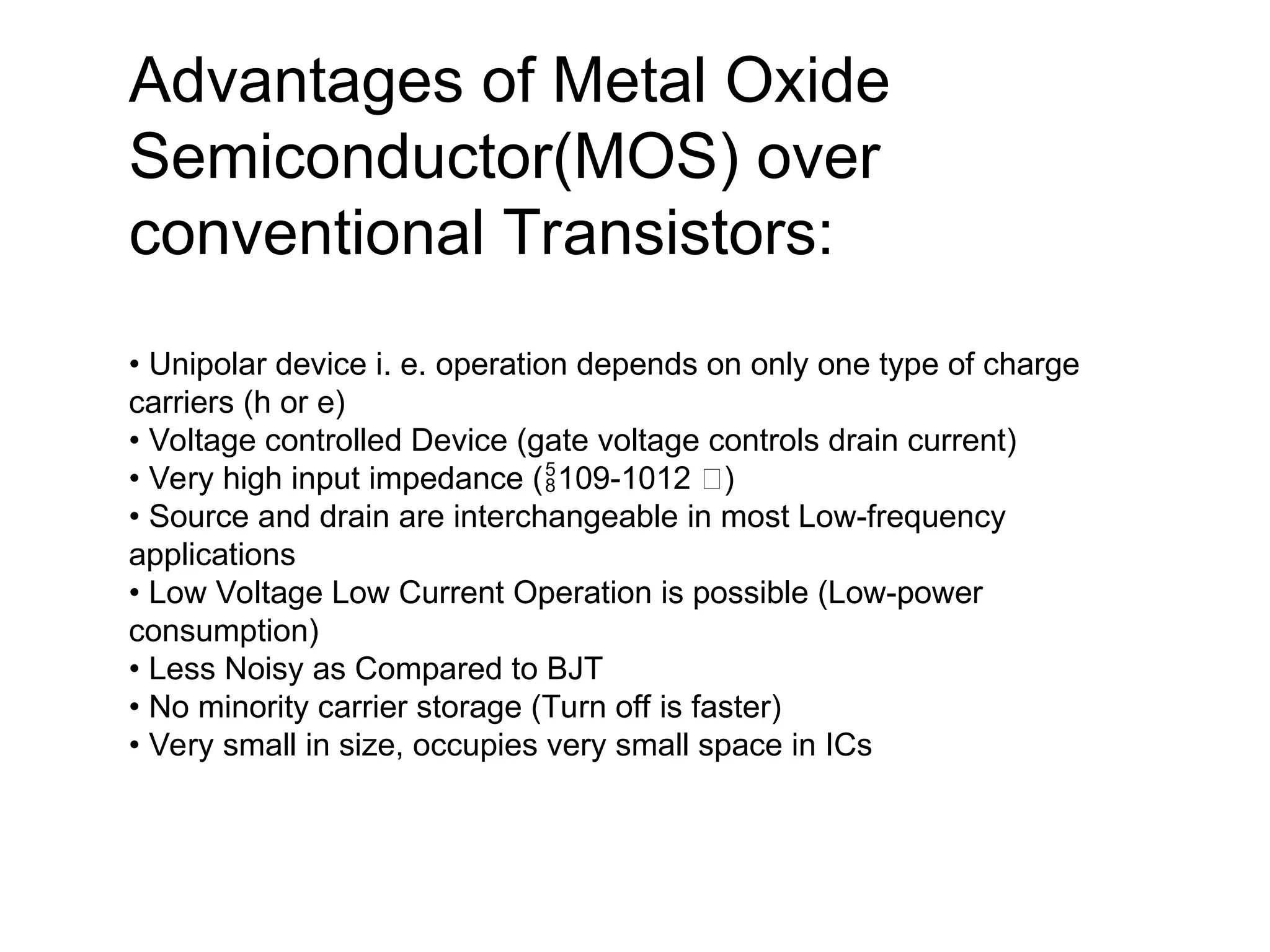
Advantages of MetalOxide
Semiconductor(MOS) over
conventional Transistors:
• Unipolar device i. e. operation depends on only one type of charge
carriers (h or e)
• Voltage controlled Device (gate voltage controls drain current)
• Very high input impedance ( 109-1012 )
• Source and drain are interchangeable in most Low-frequency
applications
• Low Voltage Low Current Operation is possible (Low-power
consumption)
• Less Noisy as Compared to BJT
• No minority carrier storage (Turn off is faster)
• Very small in size, occupies very small space in ICs
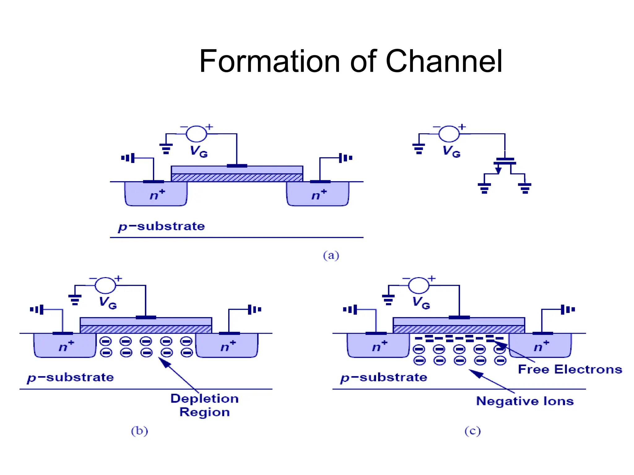
5.
METAL-OXIDE-SEMICONDUCTOR (MOS) VLSITECHNOLOGY
.
CMOS is the dominant technology, comprising of NMOS and PMOS.
Some of the examples used to illustrate the design processes will be presented
in nMOS form.
The reasons for this are as follows:
For nMOS technology, the design methodology and the design rules
are easily learned, thus providing a simple but excellent introduction to
structured design for VLSI.
nMOS technology and design processes provide an excellent
background for other technologies. In particular, some familiarity with nMOS
allows a relatively easy transition to CMOS technology design.
Not only is VLSI technology providing the user with a new and more
complex range of 'off the self' circuits, but VLSI design processes are such that
system designers can readily design their own special circuit of considerable
complexity.
6.
METAL-OXIDE-SEMICONDUCTOR (MOS) VLSITECHNOLOGY
.
CMOS is the dominant technology, comprising of NMOS and PMOS.
Some of the examples used to illustrate the design processes will be presented
in nMOS form.
The reasons for this are as follows:
For nMOS technology, the design methodology and the design rules
are easily learned, thus providing a simple but excellent introduction to
structured design for VLSI.
nMOS technology and design processes provide an excellent
background for other technologies. In particular, some familiarity with nMOS
allows a relatively easy transition to CMOS technology design.
Not only is VLSI technology providing the user with a new and more
complex range of 'off the self' circuits, but VLSI design processes are such that
system designers can readily design their own special circuit of considerable
complexity.
7.
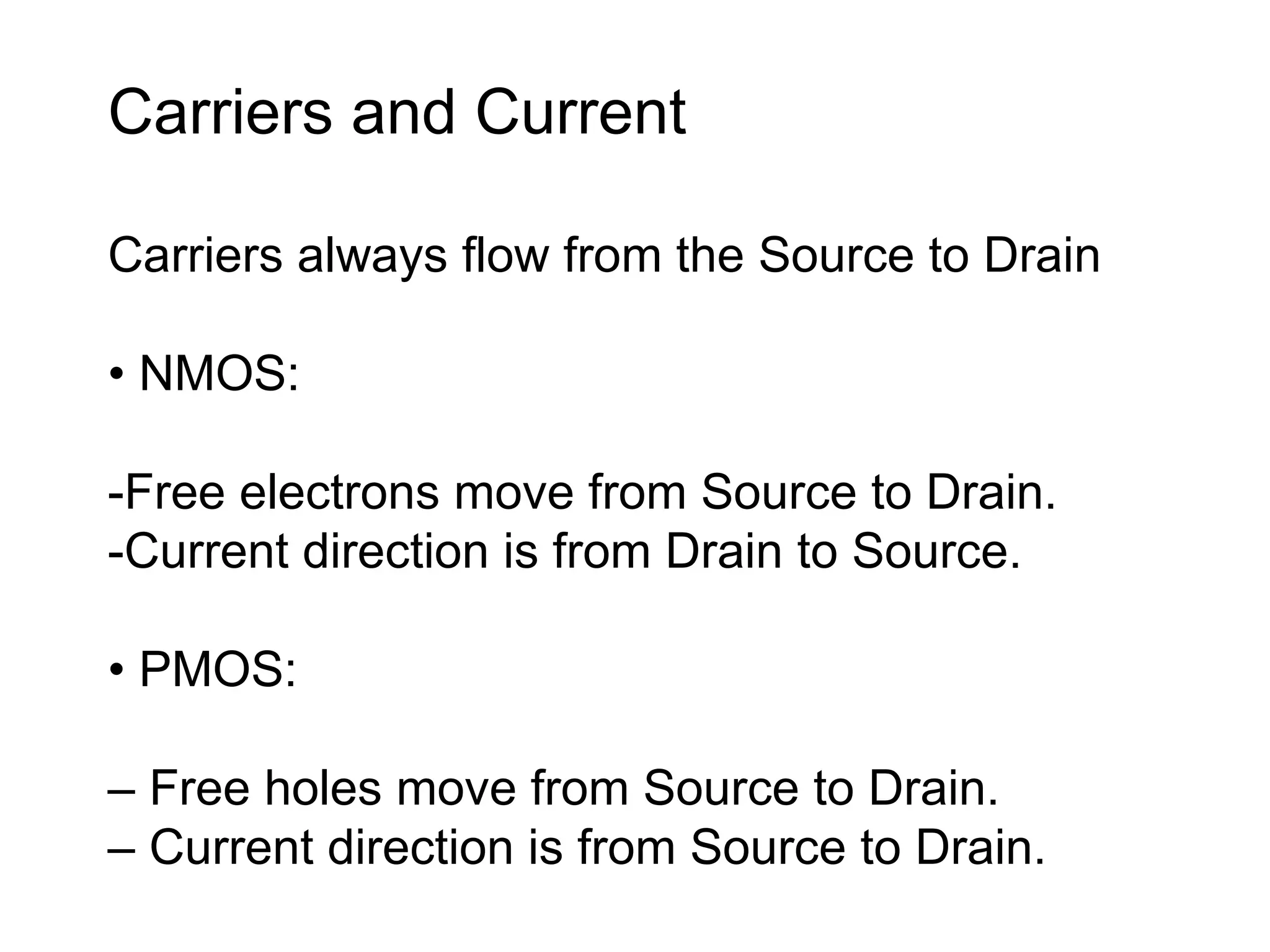
Carriers and Current
Carriersalways flow from the Source to Drain
• NMOS:
-Free electrons move from Source to Drain.
-Current direction is from Drain to Source.
• PMOS:
– Free holes move from Source to Drain.
– Current direction is from Source to Drain.
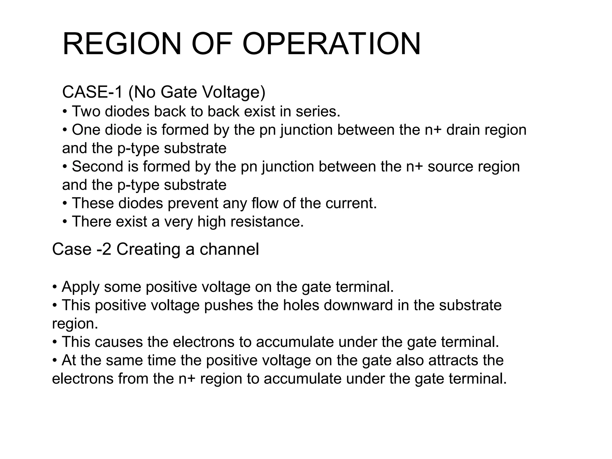
REGION OF OPERATION
CASE-1(No Gate Voltage)
• Two diodes back to back exist in series.
• One diode is formed by the pn junction between the n+ drain region
and the p-type substrate
• Second is formed by the pn junction between the n+ source region
and the p-type substrate
• These diodes prevent any flow of the current.
• There exist a very high resistance.
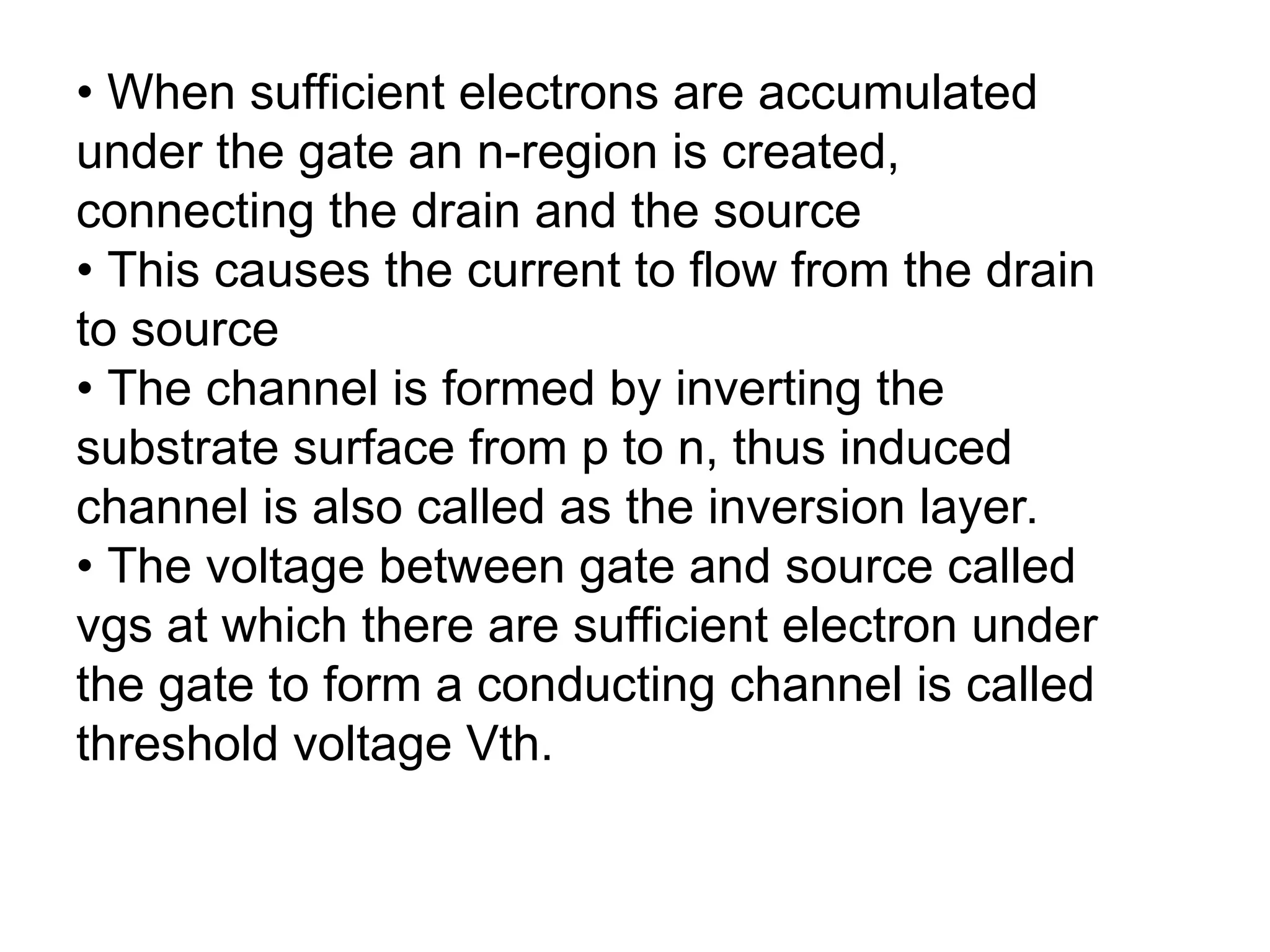
Case -2 Creating a channel
• Apply some positive voltage on the gate terminal.
• This positive voltage pushes the holes downward in the substrate
region.
• This causes the electrons to accumulate under the gate terminal.
• At the same time the positive voltage on the gate also attracts the
electrons from the n+ region to accumulate under the gate terminal.
10.
• When sufficientelectrons are accumulated
under the gate an n-region is created,
connecting the drain and the source
• This causes the current to flow from the drain
to source
• The channel is formed by inverting the
substrate surface from p to n, thus induced
channel is also called as the inversion layer.
• The voltage between gate and source called
vgs at which there are sufficient electron under
the gate to form a conducting channel is called
threshold voltage Vth.
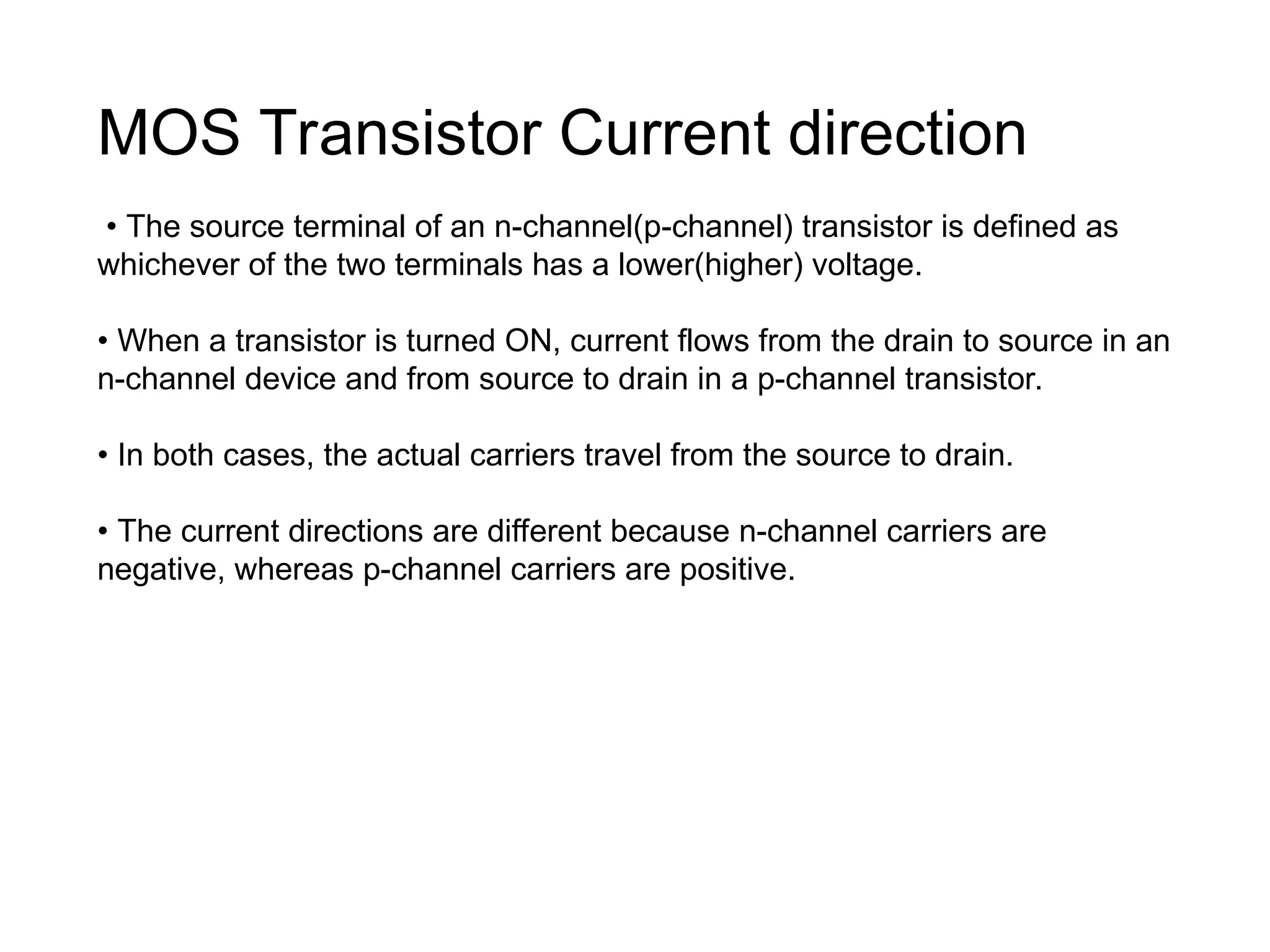
MOS Transistor Currentdirection
• The source terminal of an n-channel(p-channel) transistor is defined as
whichever of the two terminals has a lower(higher) voltage.
• When a transistor is turned ON, current flows from the drain to source in an
n-channel device and from source to drain in a p-channel transistor.
• In both cases, the actual carriers travel from the source to drain.
• The current directions are different because n-channel carriers are
negative, whereas p-channel carriers are positive.
14.
REGION OF OPERATION
1.Applying small Vds
• Now we applying some small voltage between source and drain
• The voltage Vds causes a current to flow from drain to gate.
• Now as we increase the gate voltage, more current will flow.
• Increasing the gate voltage above the threshold voltage enhances the channel,
hence this mode is called as enhancement mode operation.
2. Operation – nMOS Transistor
• Accumulation Mode - If Vgs < 0, then an electric field is
established across the substrate.
• Depletion Mode -If 0<Vgs< Vtn, the region under gate will
be depleted of charges.
• Inversion Mode – If Vgs > Vtn, the region below the gate
will be inverted.
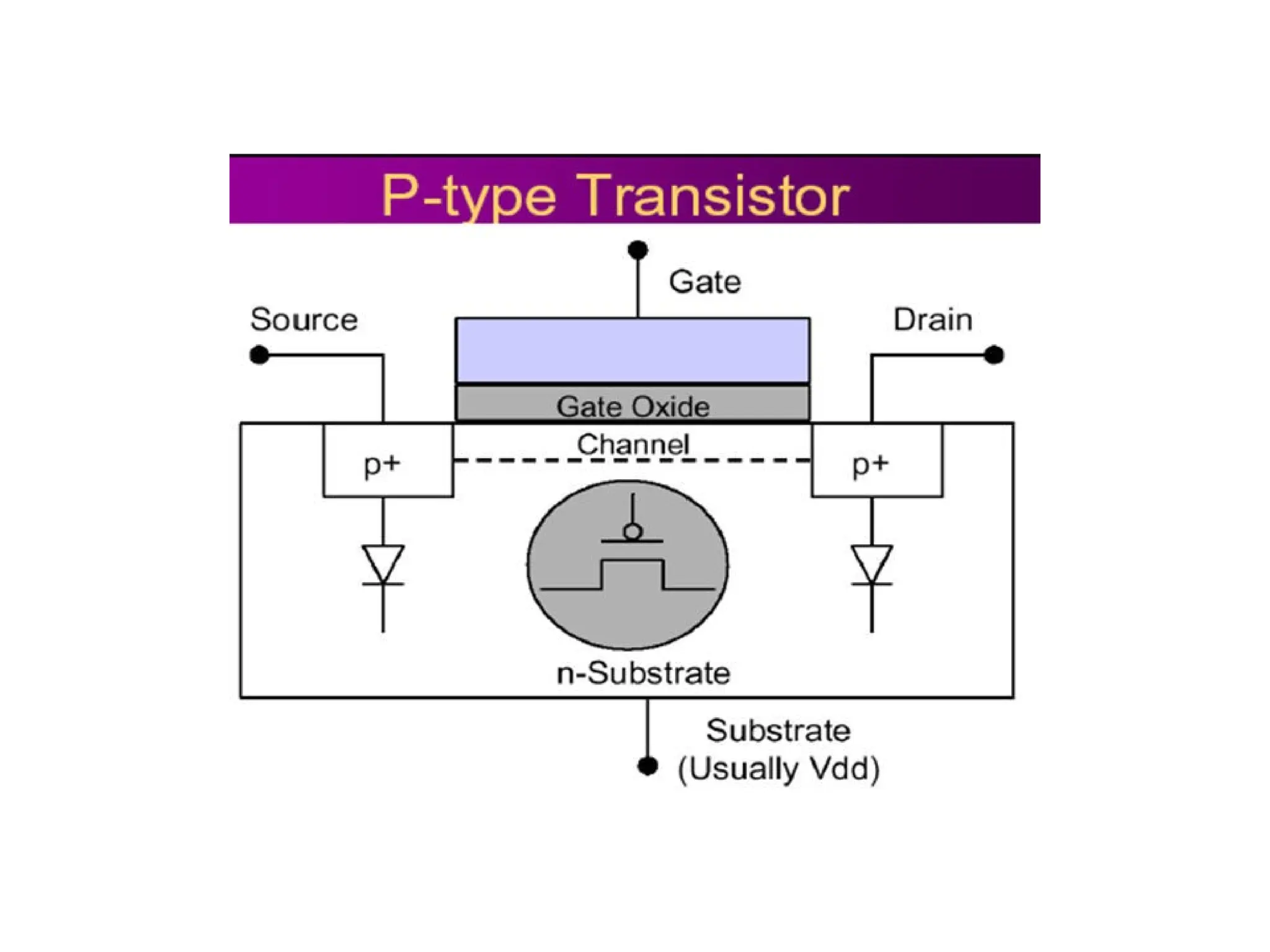
Enhancement-Mode PMOS
Transistors: Structure
•p-type source and drain regions in n-type substrate.
• vGS < 0 required to create ptype inversion layer in channel region
• For current flow, vGS < vTP
• To maintain reverse bias on source-substrate and drainsubstrate
junctions, vSB < 0 and vDB < 0
• Positive bulk-source potential causes VTP to become more negative
18.
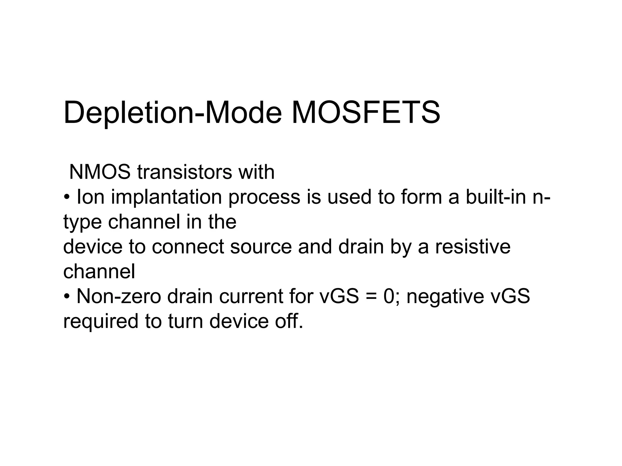
Depletion-Mode MOSFETS
NMOS transistorswith
• Ion implantation process is used to form a built-in n-
type channel in the
device to connect source and drain by a resistive
channel
• Non-zero drain current for vGS = 0; negative vGS
required to turn device off.
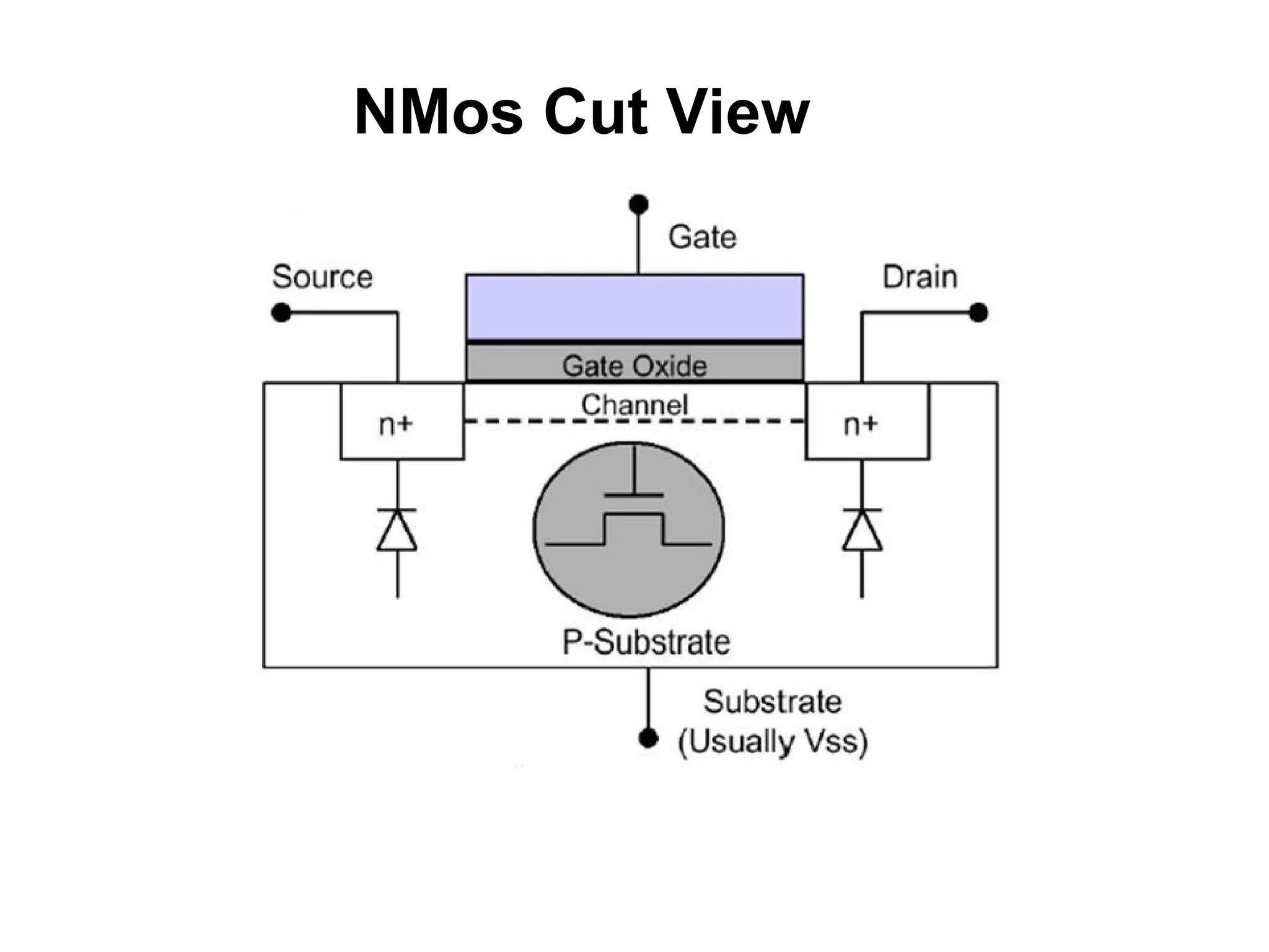
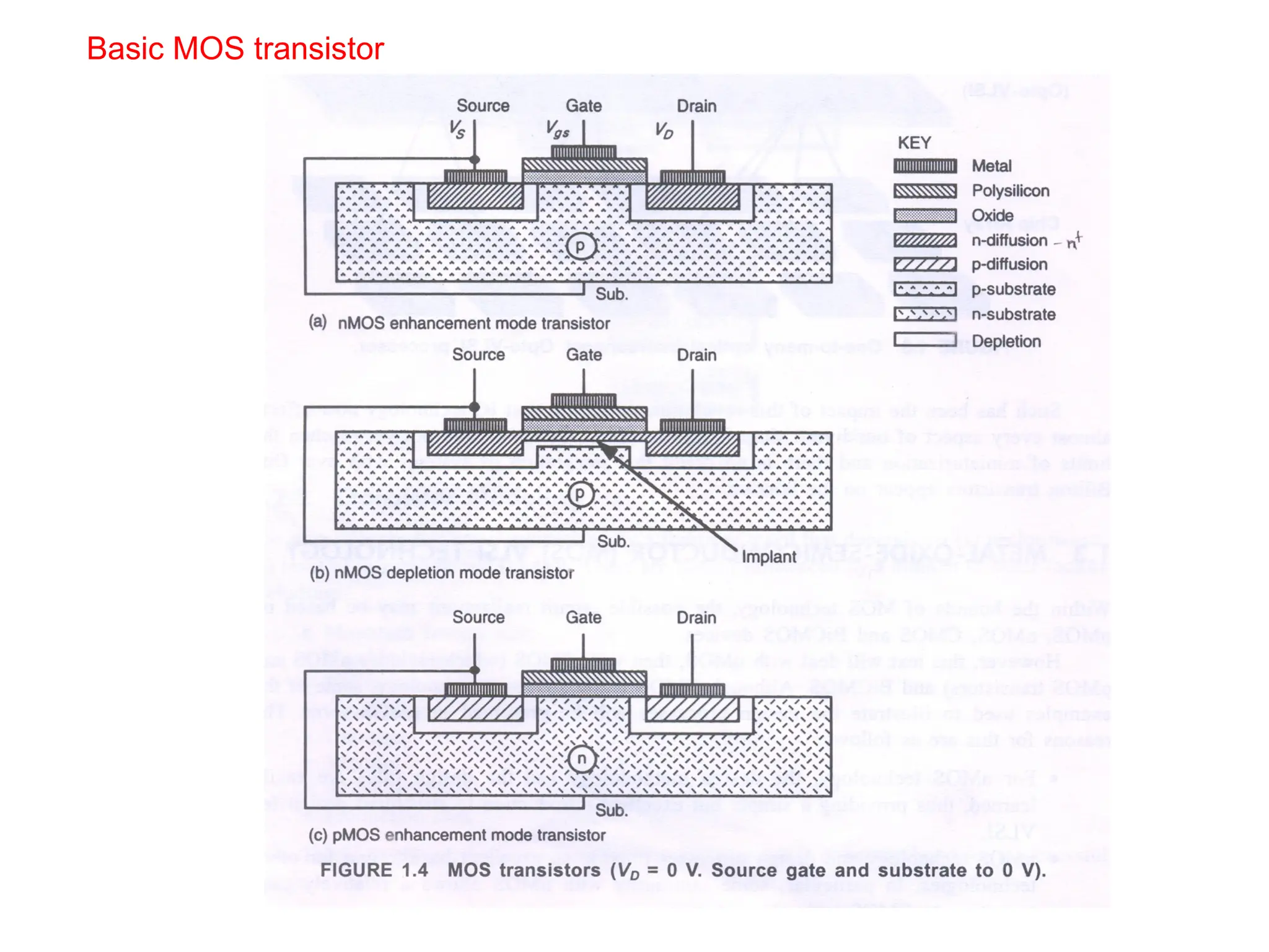
- nMOS devicesare formed in a p-type substrate of moderate doping
level. The source and drain regions are formed by diffusing n-type impurities
through suitable masks into these areas to give the desired n-impurity
concentration and give rise to depletion regions which extend mainly in the more
lightly doped p-region as shown. Thus, source and drain are isolated from one
another by two diodes.
- Connections to the source and drain are made by a deposited metal
layer. In order to make a useful device, there must be the capability for
establishing and controlling a current between source and drain, and this is
commonly achieved in one of two ways, giving rise to the enhancement mode and
depletion mode transistors.
- Consider the enhancement mode device first, shown in Figure 1.4(a).A
polysilicon gate is deposited on a layer of insulation over the region between
source and drain. Figure 1.4(a) shows a basic enhancement mode device in which
the channel is not established and the device is in a non-conducting condition, VD
= Vs = Vgs= 0.
21.
-If this gateis connected to a suitable positive voltage with respect to the
source, then the electric field established between the gate and the substrate
gives rise to a charge inversion region in the substrate under the gate
insulation and a conducting path or channel is formed between source and
drain.
-The channel may also be established so that it is present under the
condition Vgs= 0 by implanting suitable impurities in the region between
source and drain during manufacture and prior to depositing the insulation
and the gate.
-This arrangement is shown in Figure 1.4(b). Under these circumstances,
source and drain are connected by a conducting channel, but the channel
may now be closed by applying a suitable negative voltage to the gate.
-In both cases, variations of the gate voltage allow control of any current
flow between source and drain.
22.
- Figure 1.4(c)shows the basic pMOS transistor structure for an
enhancement mode device. In this case the substrate is of n-type material and the
source and drain diffusions are consequently p-type.
- In the figure, the conditions shown are those for an unbiased device;
however, the application of a negative voltage of suitable magnitude between
gate and source will give rise to the formation of a channel (p-type) between the
source and drain and current may then flow if the drain is made negative with
respect to the source. In this case the current is carried by holes as opposed to
electrons (as is the case for nMOS devices).
- In consequence, pMOS transistors are inherently slower than nMOS,
since hole mobility is less, by a factor of approximately 2.5, than electron
mobility .
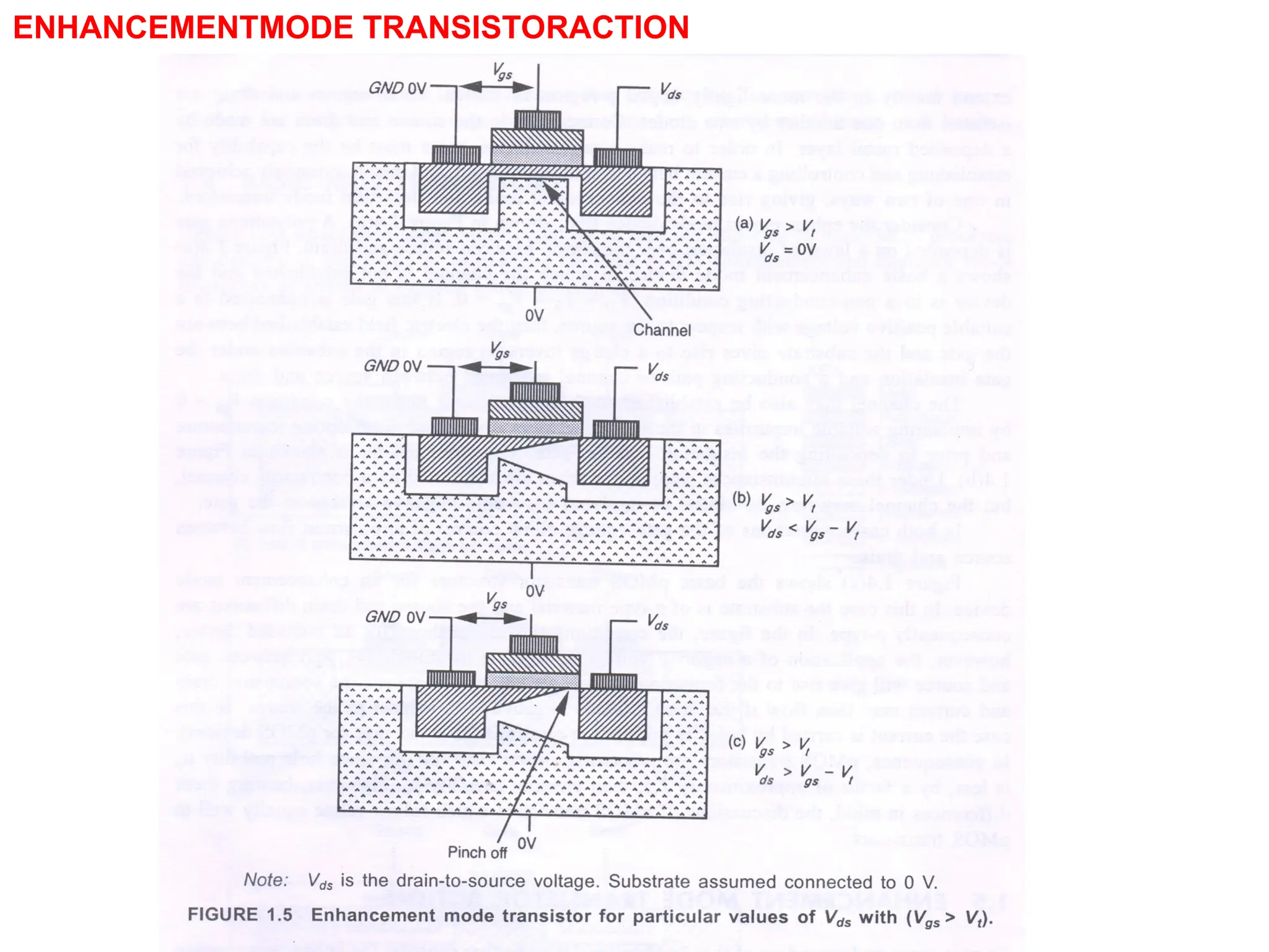
ENHANCEMENTMODE TRANSISTORACTION
Consider theenhancement mode device, as in Figure 1.5,
under three sets of conditions.
1. In order to establish the channel in the first place, a
minimum voltage level of threshold voltage Vt must be established
between gate and source (and of course between gate and substrate as
a result). Figure 1.5(a) then indicates the conditions prevailing with
the channel established but no current flowing between source and
drain (Vds = 0).
2. Now consider the conditions prevailing when current
flows in the channel by applying a voltage Vds between drain and
source. There must be a corresponding IR drop = Vds along the
channel. This results in the voltage between gate and channel varying
with distance along the channel with the voltage being a maximum of
Vgs at the source end.
25.
Since the effectivegate voltage is Vg = Vgs- Vt (no current flows when
Vgs< Vt), there will be voltage available to invert the channel at the drain end so
long as Vgs - Vt Vds. 'The limiting condition comes when Vds = Vgs - Vt, For
all voltages Vds < Vgs - Vt the device is in the non-saturated region of operation
which is the condition shown in Figure l.5(b).
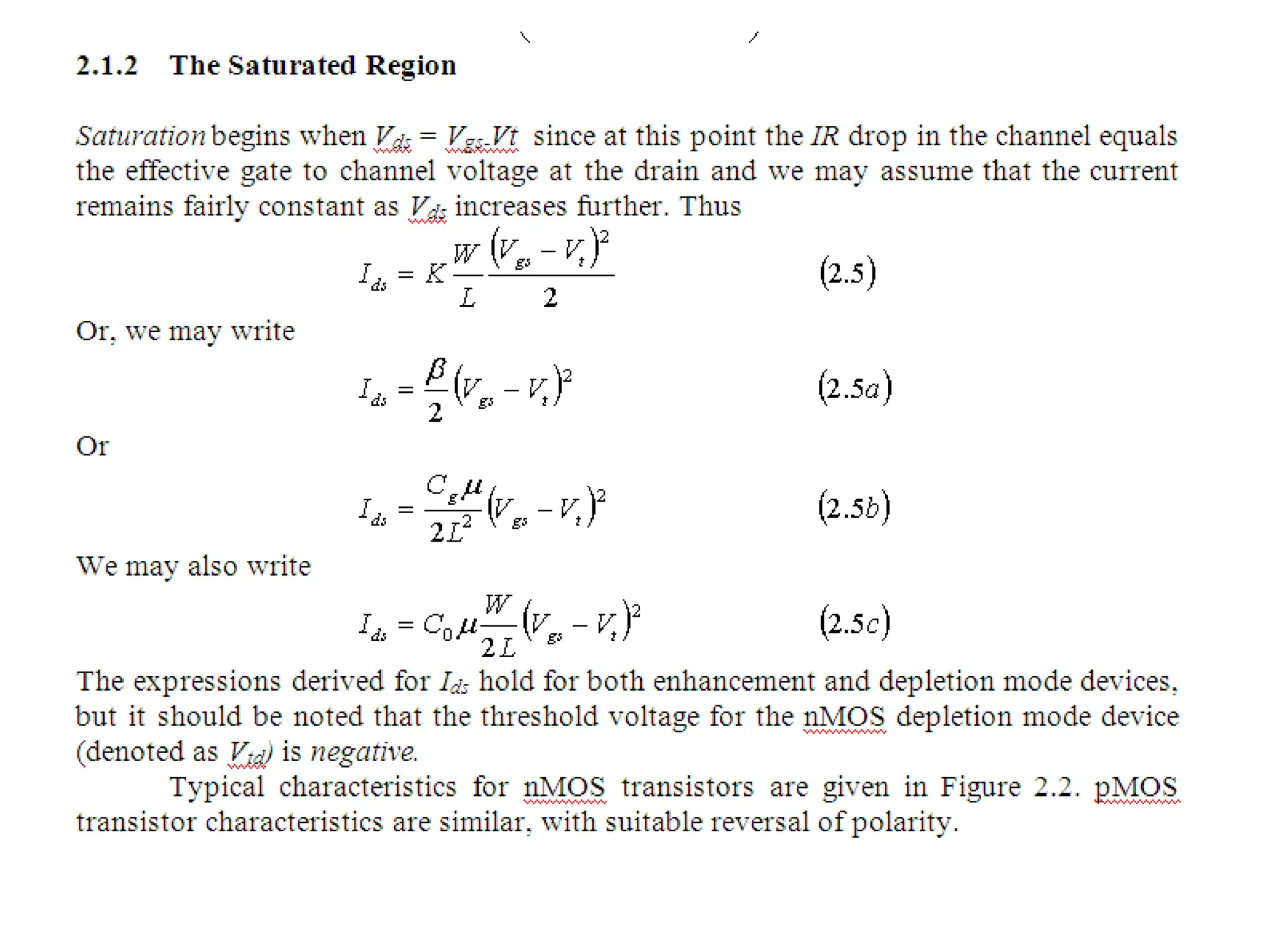
3. Consider now what happens when Vds is increased to a level greater
than Vgs- Vt In this case, an IR drop = Vgs- Vt takes place over less than the
whole length of the channel so that over part of the channel, near the drain, there is
insufficient electric field available to give rise to an inversion layer to create the
channel. The channel is therefore 'pinched off', as indicated in Figure 1.5(c).
Diffusion current completes the path from source to drain in this case,
causing the channel to exhibit a high resistance and behave as a constant current
source. This region, known as saturation, is characterized by almost constant
current for increase of Vds above Vds= Vgs- Vt.
In all cases, the channel will cease to exist and no current will flow when
Vgs < Vt. Typically, for enhancement mode devices, Vt = 1 volt for VDD = 5
volt or, in general terms, Vt = 0.2VDD.
26.
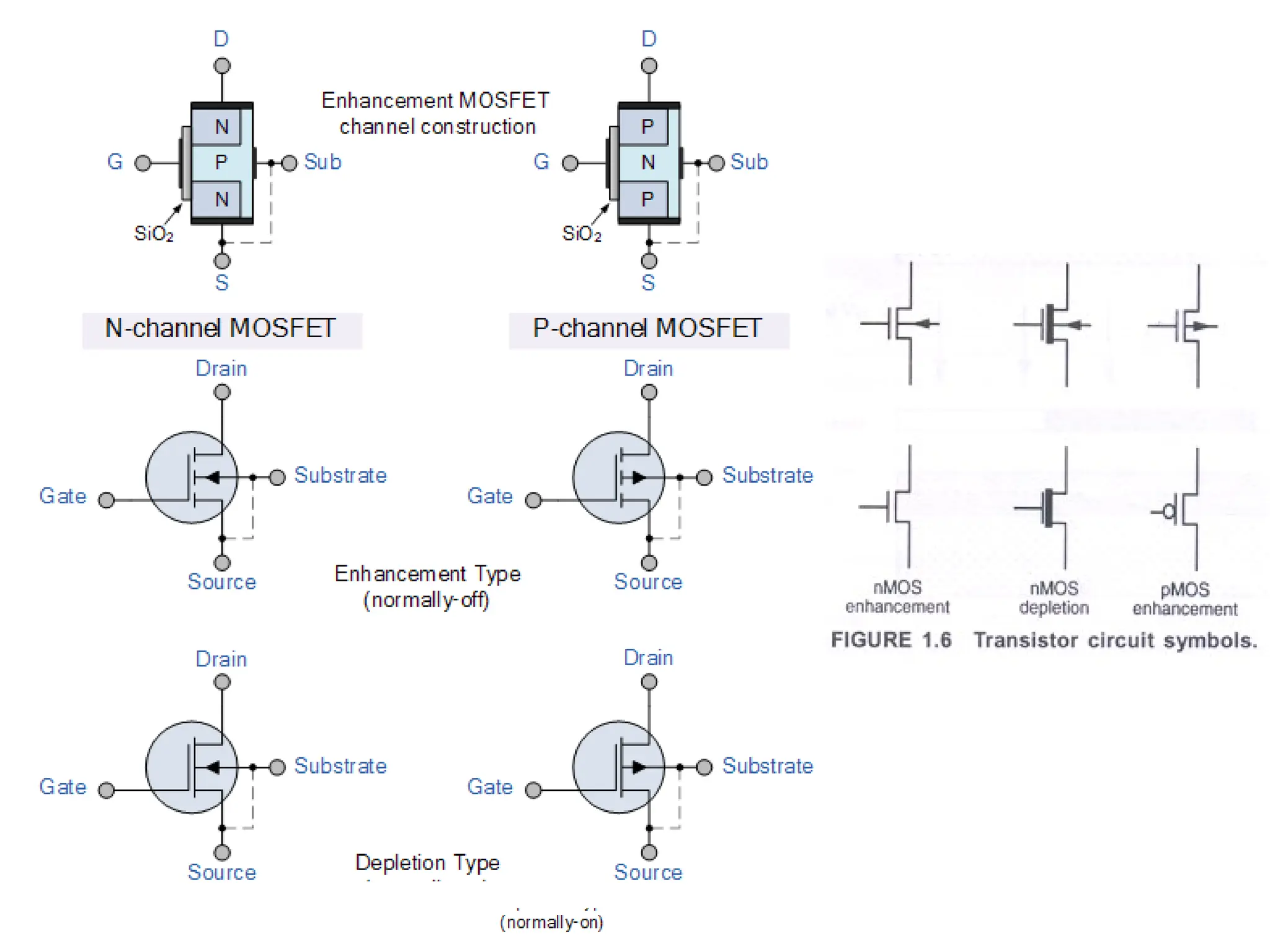
DEPLETION MODE TRANSISTORACTION
For depletion mode devices the channel is established,
because of the implant, even when Vgs = 0, and to cause the channel
to cease to exist a negative voltage Vtd must be applied between
gate and source.
Vtd is typically < -0.8VDD,depending on the implant and
substrate bias, but, threshold voltage differences aside, the action is
similar to that of the enhancement mode transistor. Commonly used
symbols for nMOS and pMOS transistors are set out in Figure 1.6.
29.
nMOS fabrication steps
1.Processing is carried out on a thin wafer cut from a single crystal of silicon of high purity into which
the required p-impurities are introduced as the crystal is grown.
2. A layer of silicon dioxide (Si02) is grown all over the surface of the wafer to protect the surface, act
as a barrier to dopants during processing, and provide a generally insulating substrate on to which
other layers may be deposited and patterned.
3. The surface is now covered with a photoresist which is deposited onto the wafer and spun to
achieve an even distribution of the required thickness.
4. The photoresist layer is then exposed to ultraviolet light through a mask which defines those
regions into which diffusion is to take place together with transistor channels.
5. These areas are subsequently readily etched away together with the underlying silicon dioxide so
that the wafer surface is exposed in the window defined by the mask.
6. The remaining photoresist is removed and a thin layer of Si02 is grown over the entire chip surface
and then polysilicon is deposited on top of this to form the gate structure.
7. Further photoresist coating and masking allows the polysilicon to be patterned (as shown in Step 6)
and then the thin oxide is removed to expose areas into which
8. Thick oxide (Si02) is grown over all again and is then masked with photoresist and etched to
expose
selected areas of the polysilicon gate and the drain and source areas where connections (i.e. contact
cuts) are to be made.
9. The whole chip then has metal (aluminium) deposited over its surface. This metal layer is then
masked and etched to form the required interconnection pattern.
30.
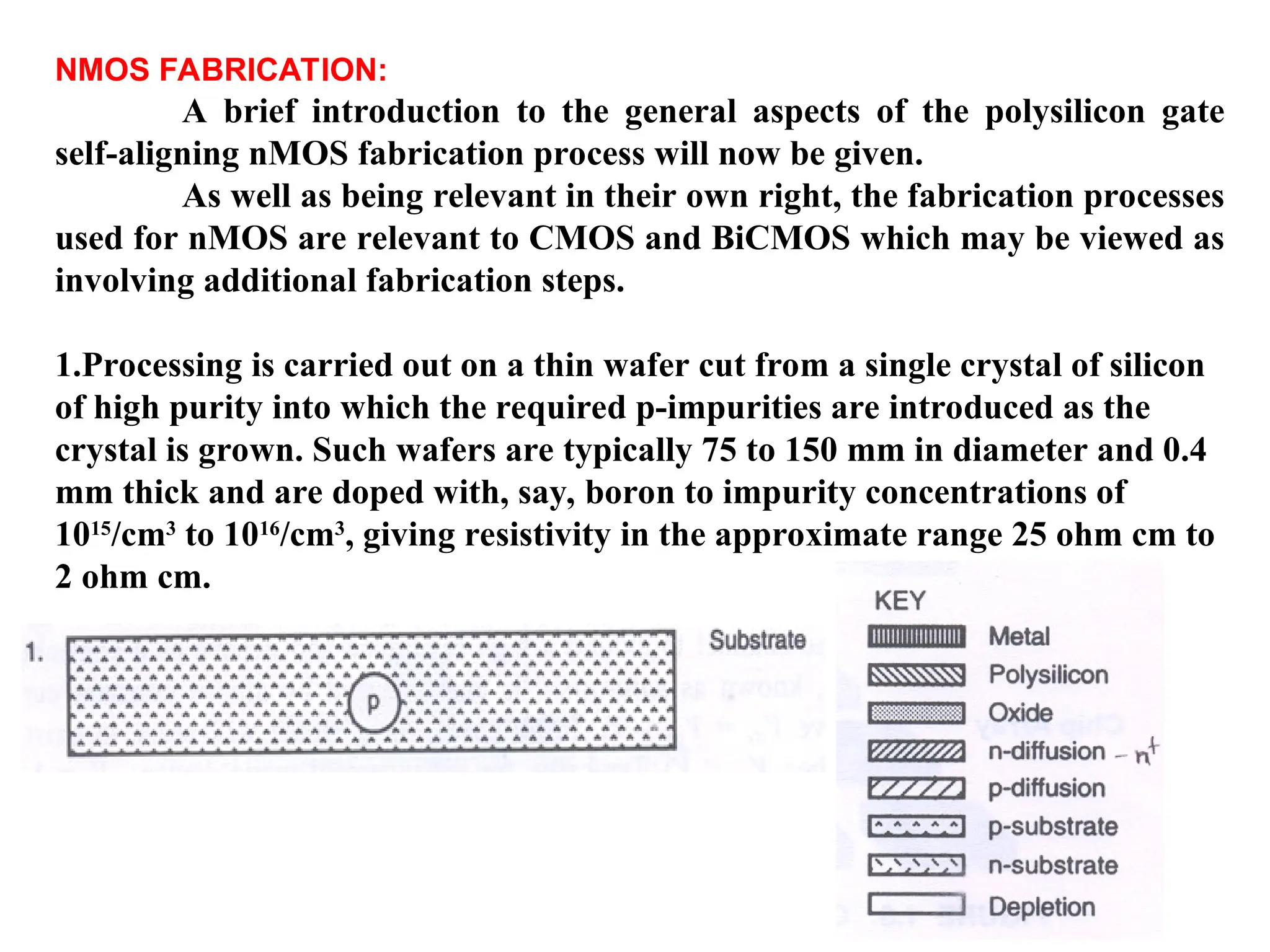
NMOS FABRICATION:
A briefintroduction to the general aspects of the polysilicon gate
self-aligning nMOS fabrication process will now be given.
As well as being relevant in their own right, the fabrication processes
used for nMOS are relevant to CMOS and BiCMOS which may be viewed as
involving additional fabrication steps.
1.Processing is carried out on a thin wafer cut from a single crystal of silicon
of high purity into which the required p-impurities are introduced as the
crystal is grown. Such wafers are typically 75 to 150 mm in diameter and 0.4
mm thick and are doped with, say, boron to impurity concentrations of
1015
/cm3
to 1016
/cm3
, giving resistivity in the approximate range 25 ohm cm to
2 ohm cm.
32.
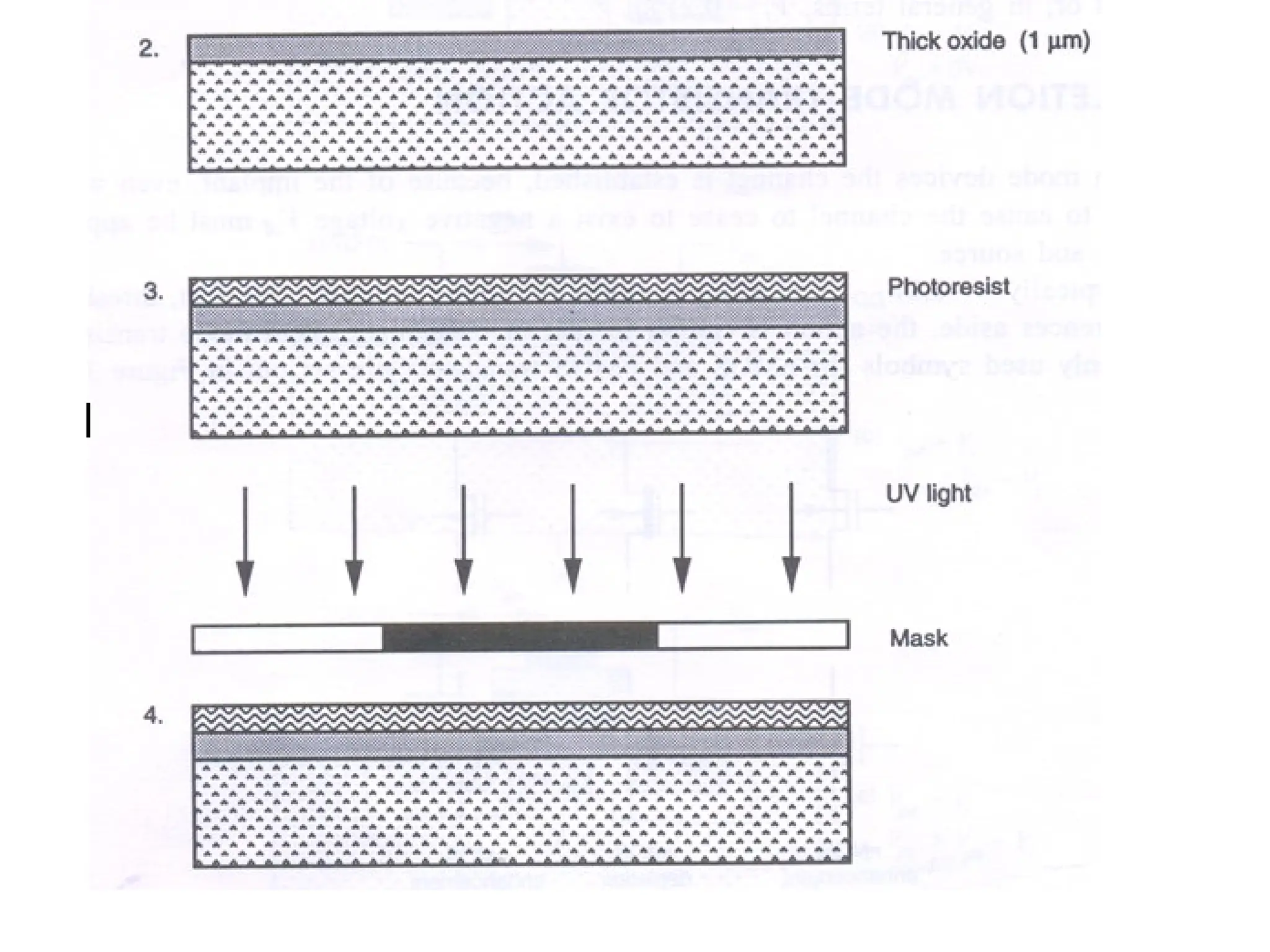
2. A layerof silicon dioxide (SiO2), typically 1 thick, is grown all
over the surface of the wafer to protect the surface, act as a barrier
to dopants during processing, and provide a generally insulating
substrate onto which other layers may be deposited and patterned.
3. The surface is now covered with a photoresist which is deposited
onto the wafer and spun to achieve an even distribution of the
required thickness.
4. The photoresist layer is then exposed to ultraviolet light through
a mask which defines those regions into which diffusion is to take
place together with transistor channels. Assume, for example, that
those areas exposed to ultraviolet radiation are polymerized
(hardened), but that the areas required for diffusion are shielded by
the mask and remain unaffected.
33.
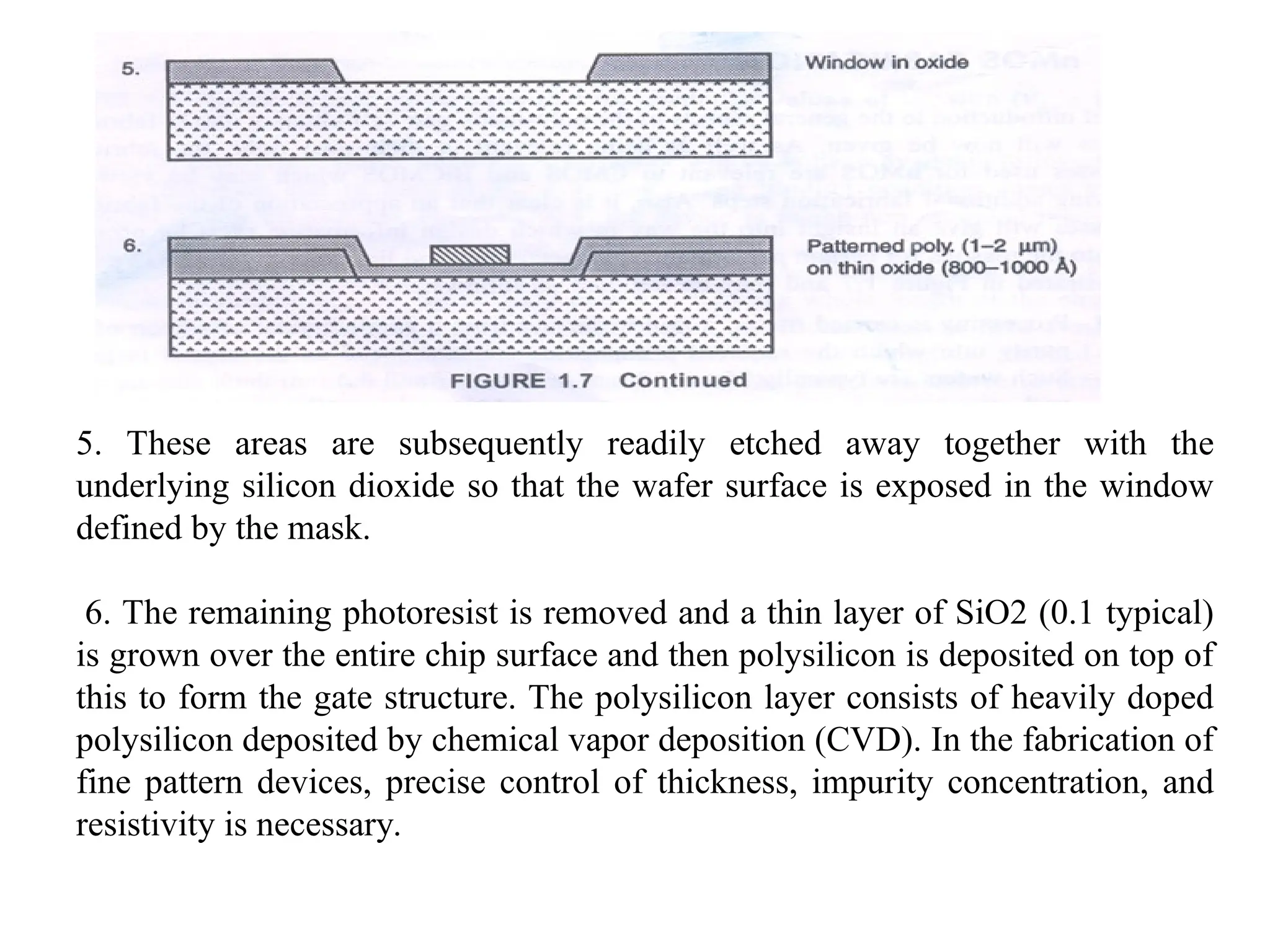
5. These areasare subsequently readily etched away together with the
underlying silicon dioxide so that the wafer surface is exposed in the window
defined by the mask.
6. The remaining photoresist is removed and a thin layer of SiO2 (0.1 typical)
is grown over the entire chip surface and then polysilicon is deposited on top of
this to form the gate structure. The polysilicon layer consists of heavily doped
polysilicon deposited by chemical vapor deposition (CVD). In the fabrication of
fine pattern devices, precise control of thickness, impurity concentration, and
resistivity is necessary.
34.
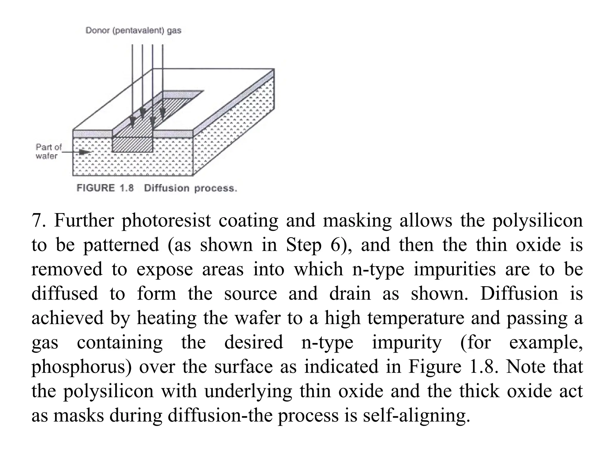
7. Further photoresistcoating and masking allows the polysilicon
to be patterned (as shown in Step 6), and then the thin oxide is
removed to expose areas into which n-type impurities are to be
diffused to form the source and drain as shown. Diffusion is
achieved by heating the wafer to a high temperature and passing a
gas containing the desired n-type impurity (for example,
phosphorus) over the surface as indicated in Figure 1.8. Note that
the polysilicon with underlying thin oxide and the thick oxide act
as masks during diffusion-the process is self-aligning.
36.
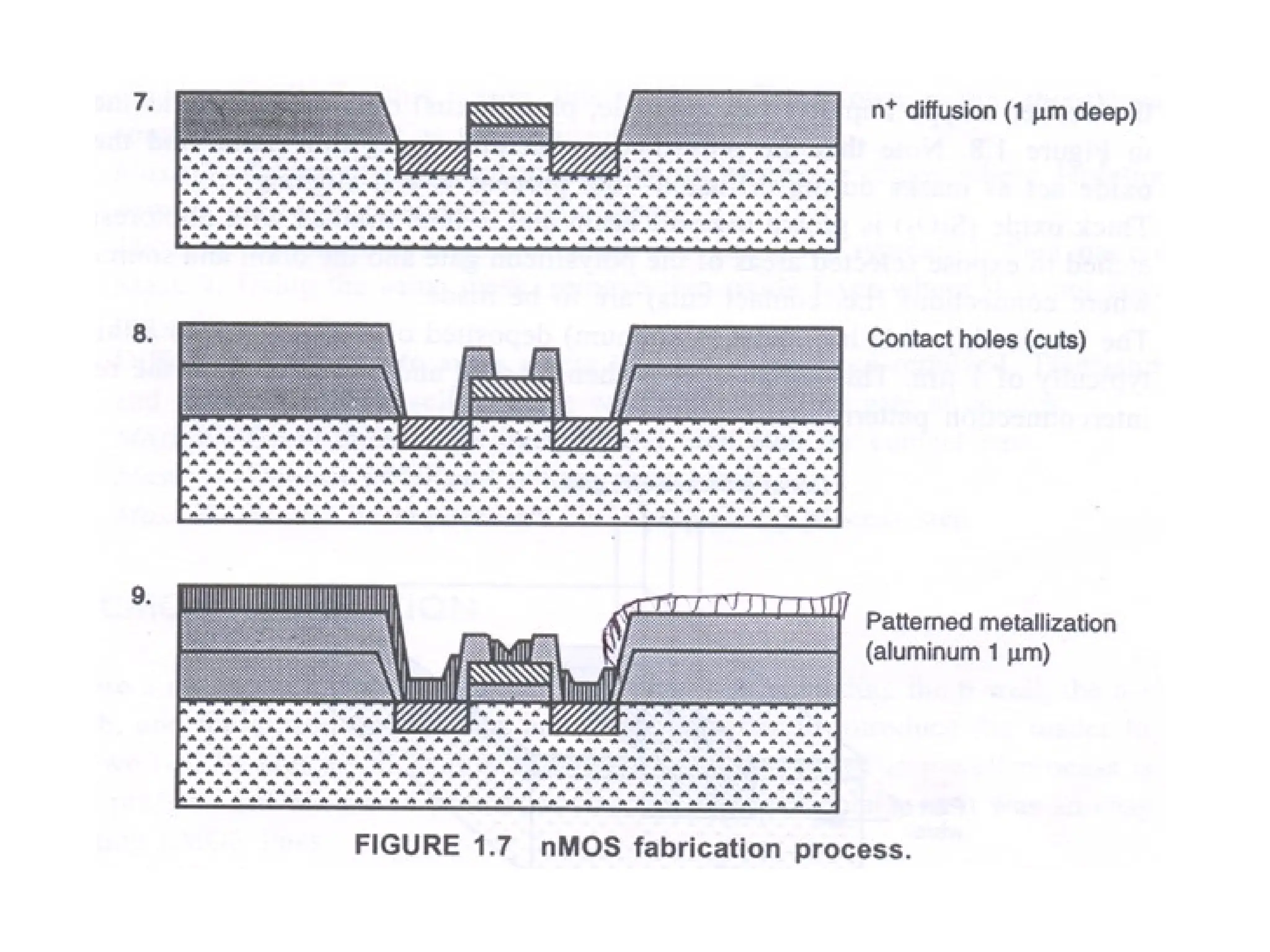
8. Thick oxide(SiO2) is grown over all again and is then masked with
photoresist and etched to expose selected areas of the polysilicon gate
and the drain and source areas where connections (i.e. contact cuts) are
to be made.
9. The whole chip then has metal (aluminum) deposited over its surface to
a thickness typically of 1 11m.This metal layer is then masked and etched
to form the required interconnection pattern.
Process revolves around the formation or deposition and
patterning of three layers, separated by silicon dioxide insulation. The
layers are diffused within the substrate, polysilicon on oxide, on the
substrate, and metal insulated again by oxide.
To form depletion mode devices it is only necessary to introduce
a masked ion implantation step between Steps 5 and 6 in Figure 1.7.
Again, the thick oxide acts as a mask and this process stage is also self-
aligning.
37.
Summary of annMOS Process
Processing takes place on a p-doped silicon crystal wafer on which is grown a 'thick'
layer of SiO2.
Mask 1-Pattern SiO2 to expose the silicon surface in areas where paths in the
diffusion layer or source, drain or gate areas of transistors are required. Deposit thin
oxide over all. For this reason, this mask is often known as the 'thinox' mask but
some texts refer to it as the diffusion mask.
Mask 2-Pattern the ion implantation within the thinox region where depletion mode
devices are to be produced-self--aligning.
Mask 3-Deposit polysilicon over all (1.5 m thick typically), then pattern using Mask
3. Using the same mask, remove thin oxide layer where it is not covered by
polysilicon.
Diffuse n+
regions into areas where thin oxide has been removed. Transistor drains
and sources are thus self-aligning with respect to the gate structures.
Mask 4-Grow thick oxide over all and then etch for contact cuts.
Mask 5-Deposit metal and pattern with Mask 5.
Mask 6-Would be required for the overglassing process step.
38.
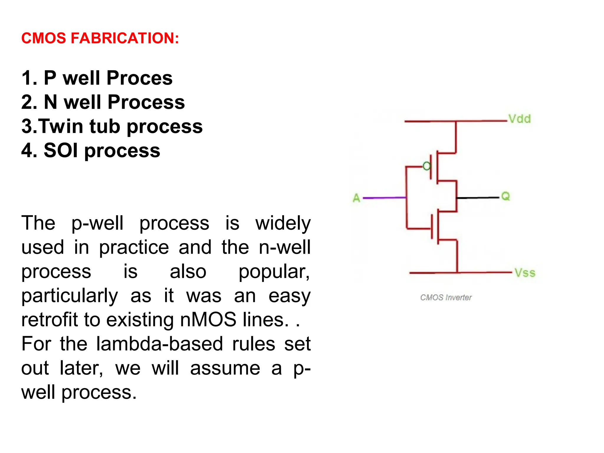
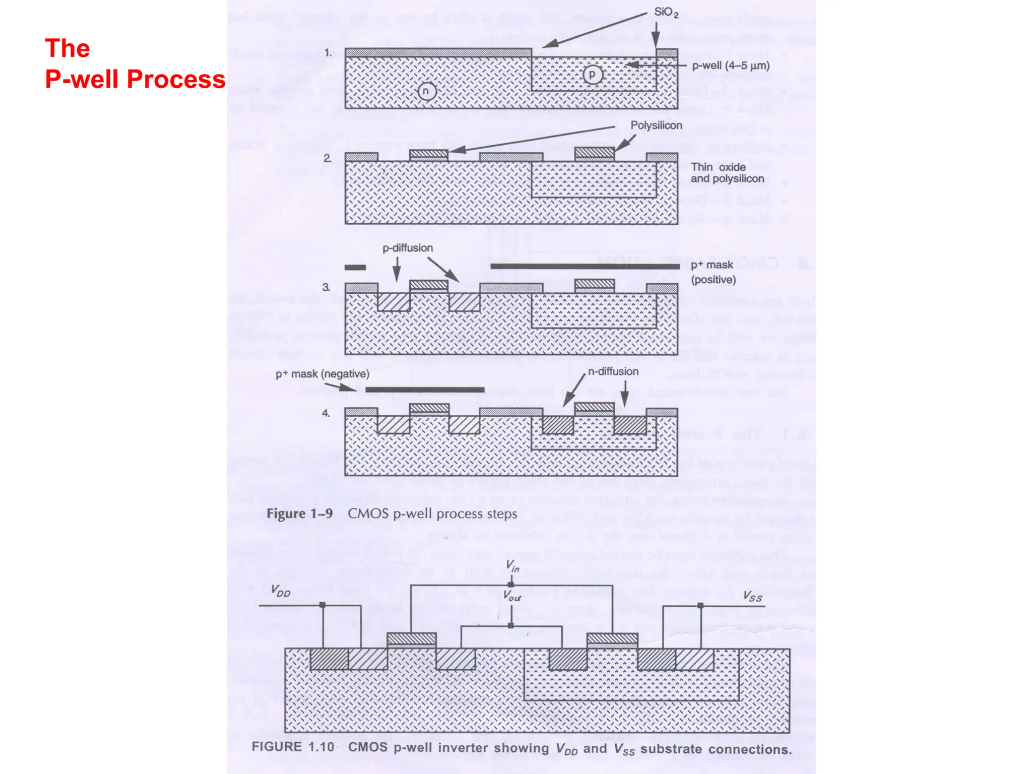
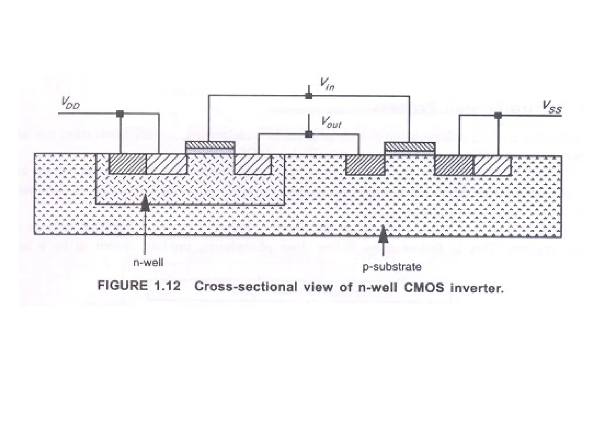
CMOS FABRICATION:
1. Pwell Proces
2. N well Process
3.Twin tub process
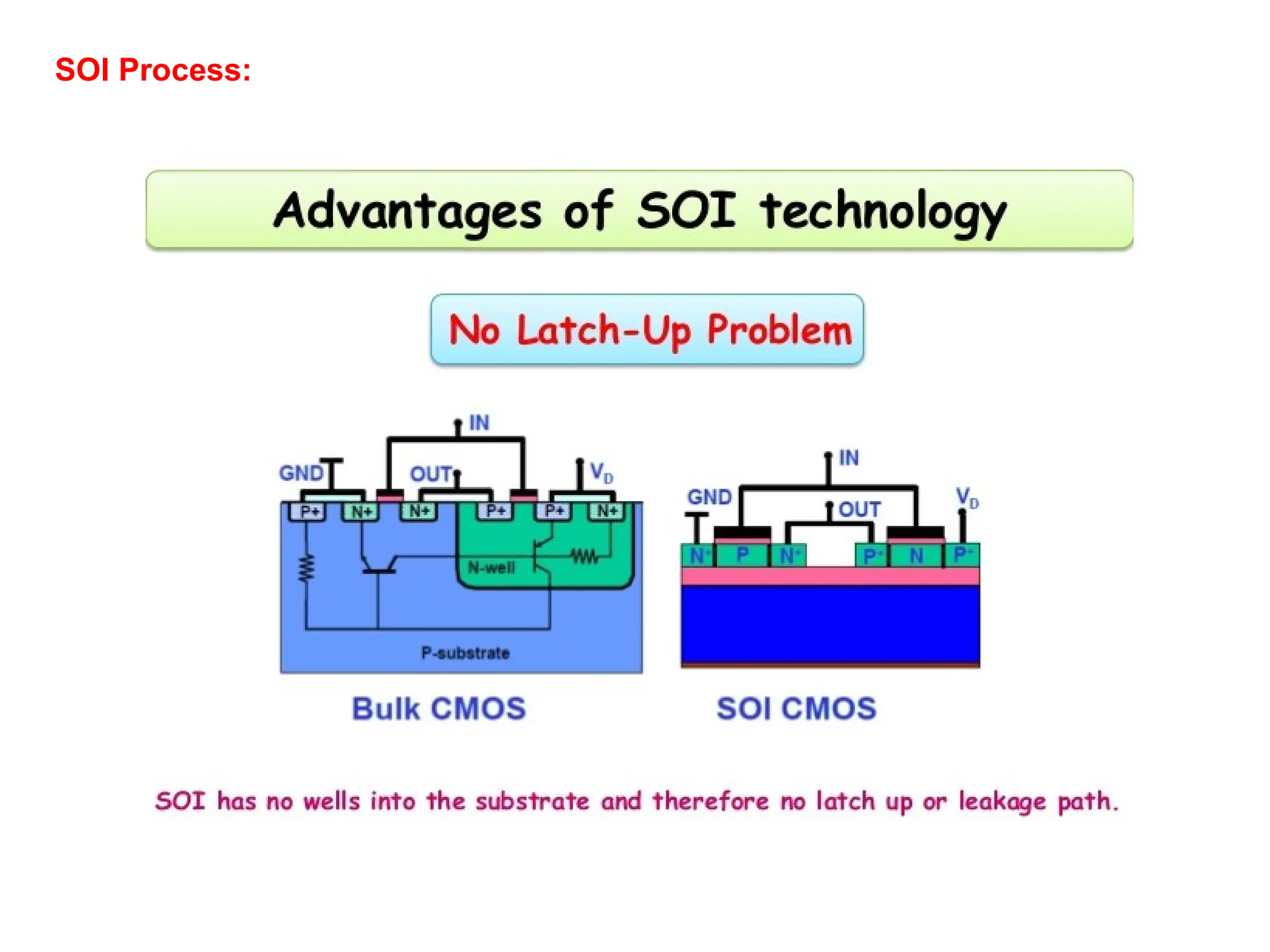
4. SOI process
The p-well process is widely
used in practice and the n-well
process is also popular,
particularly as it was an easy
retrofit to existing nMOS lines. .
For the lambda-based rules set
out later, we will assume a p-
well process.
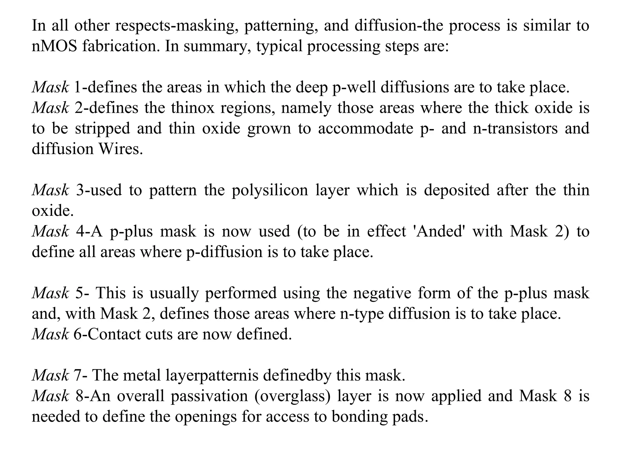
In all otherrespects-masking, patterning, and diffusion-the process is similar to
nMOS fabrication. In summary, typical processing steps are:
Mask 1-defines the areas in which the deep p-well diffusions are to take place.
Mask 2-defines the thinox regions, namely those areas where the thick oxide is
to be stripped and thin oxide grown to accommodate p- and n-transistors and
diffusion Wires.
Mask 3-used to pattern the polysilicon layer which is deposited after the thin
oxide.
Mask 4-A p-plus mask is now used (to be in effect 'Anded' with Mask 2) to
define all areas where p-diffusion is to take place.
Mask 5- This is usually performed using the negative form of the p-plus mask
and, with Mask 2, defines those areas where n-type diffusion is to take place.
Mask 6-Contact cuts are now defined.
Mask 7- The metal layerpatternis definedby this mask.
Mask 8-An overall passivation (overglass) layer is now applied and Mask 8 is
needed to define the openings for access to bonding pads.
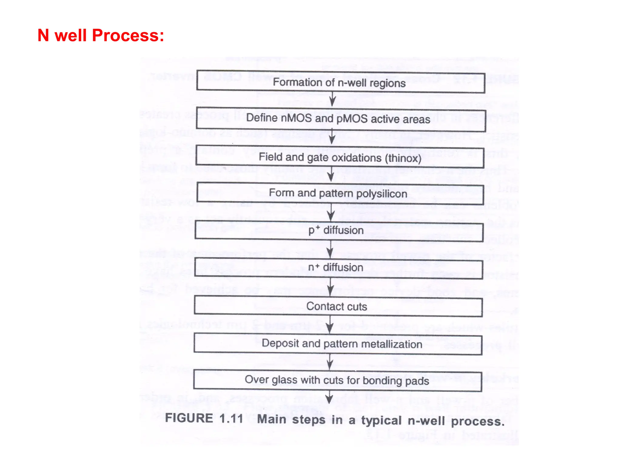
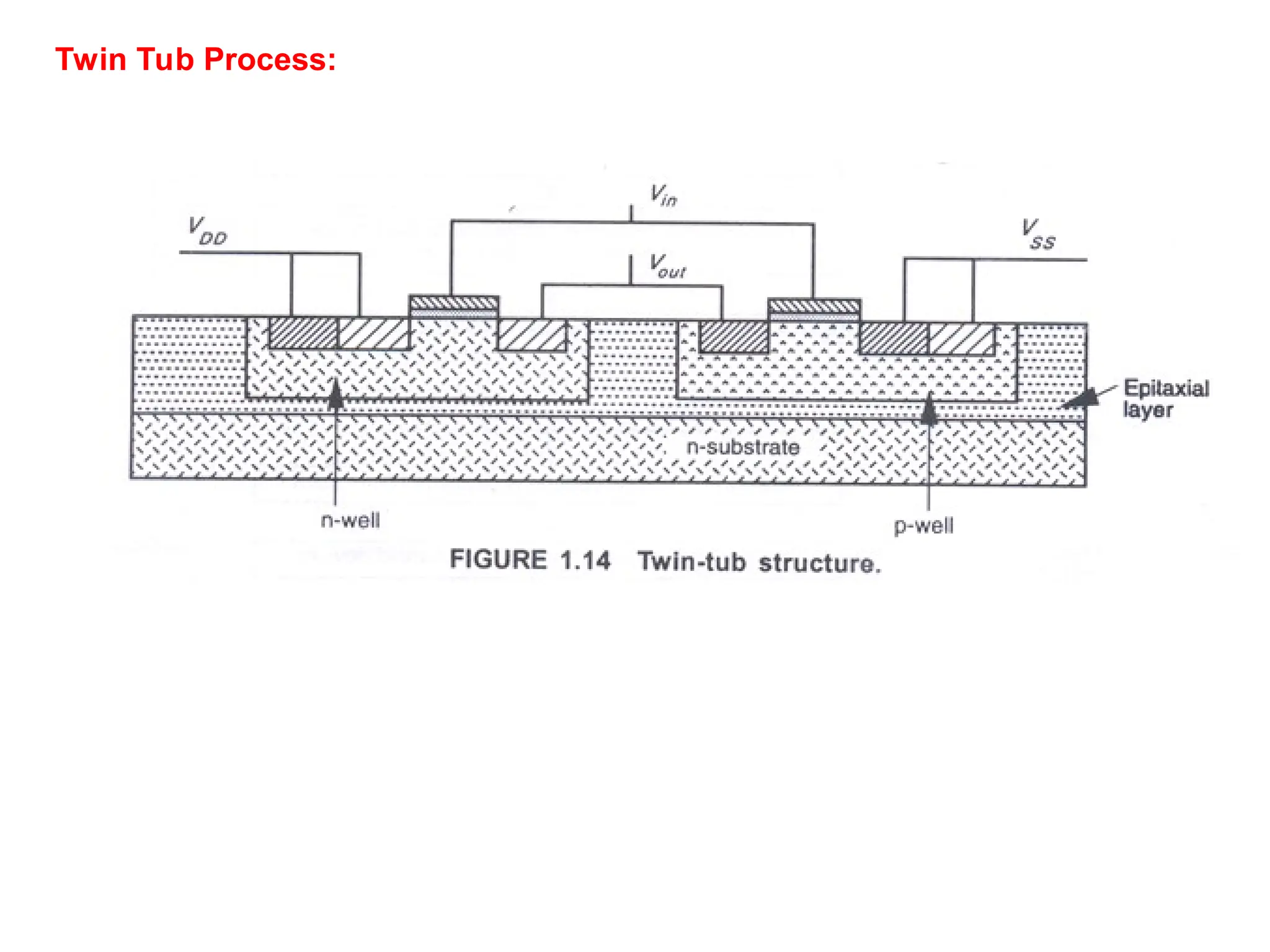
The twin-tub-Tub Process
Alogical extension of the p-well and n-well approaches
is the twin-tub fabrication process.
-start with a substrate of high resistivity n-type material
-then create both .. n-well and p-well regions.
- Through this process it is possible to preserve the
performance of n-transistors without compromising the
p-transistors.
- Doping control is more readily achieved and some
relaxation in manufacturing tolerances results.
- This is particularly important as far as latch-up is
concerned.
Features
- The objectiveof the Bi-CMOS is to combine bipolar and CMOS so
as to exploit the advantages of both the technologies.
- Today Bi-CMOS has become one of the dominant technologies
used for high speed, low power and highly functional VLSI circuits.
- The process step required for both CMOS and bipolar are almost
similar
- The primary approach to realize high performance Bi-CMOS devices
is the addition of bipolar process steps to a baseline CMOS process.
- The Bi-CMOS gates could be used as an effective way of speeding
up the VLSI circuits.
- The applications of Bi-CMOS are vast.
- Advantages of bipolar and CMOS circuits can be retained in Bi-
CMOS chips.
- Bi-CMOS technology enables high performance integrated circuits
IC’s but increases process complexity.
47.
BiCMOS TECHNOLOGY
The deficiencyof MOS technology lies in the limited load driving
capabilities of MOS transistors. This is due to the limited current sourcing and
current sinking abilities associated with both p- and n-transistors and although it is
possible, for example, to design so-called super buffers using MOS transistors
alone, such arrangements do not always compare well with the capabilities of
bipolar transistors.
Bipolar transistors also provide higher gain and have generally better
noise and high frequency characteristics than MOS transistors. Using BiCMOS
gates may be an effective way of speeding up VLSI circuits. However, the
application of BiCMOS in subsyste1Jls such as ALU, ROM, a register-file, or, for
that matter, a barrel shifter is not always an effective way of improving speed. This
is because most gates in such structures do not have to drive large capacitive loads
so that the BiCMOS arrangements give no speed advantage.
To take advantage of BiCMOS, the whole functional entity, not just the
logic gates, must be considered.
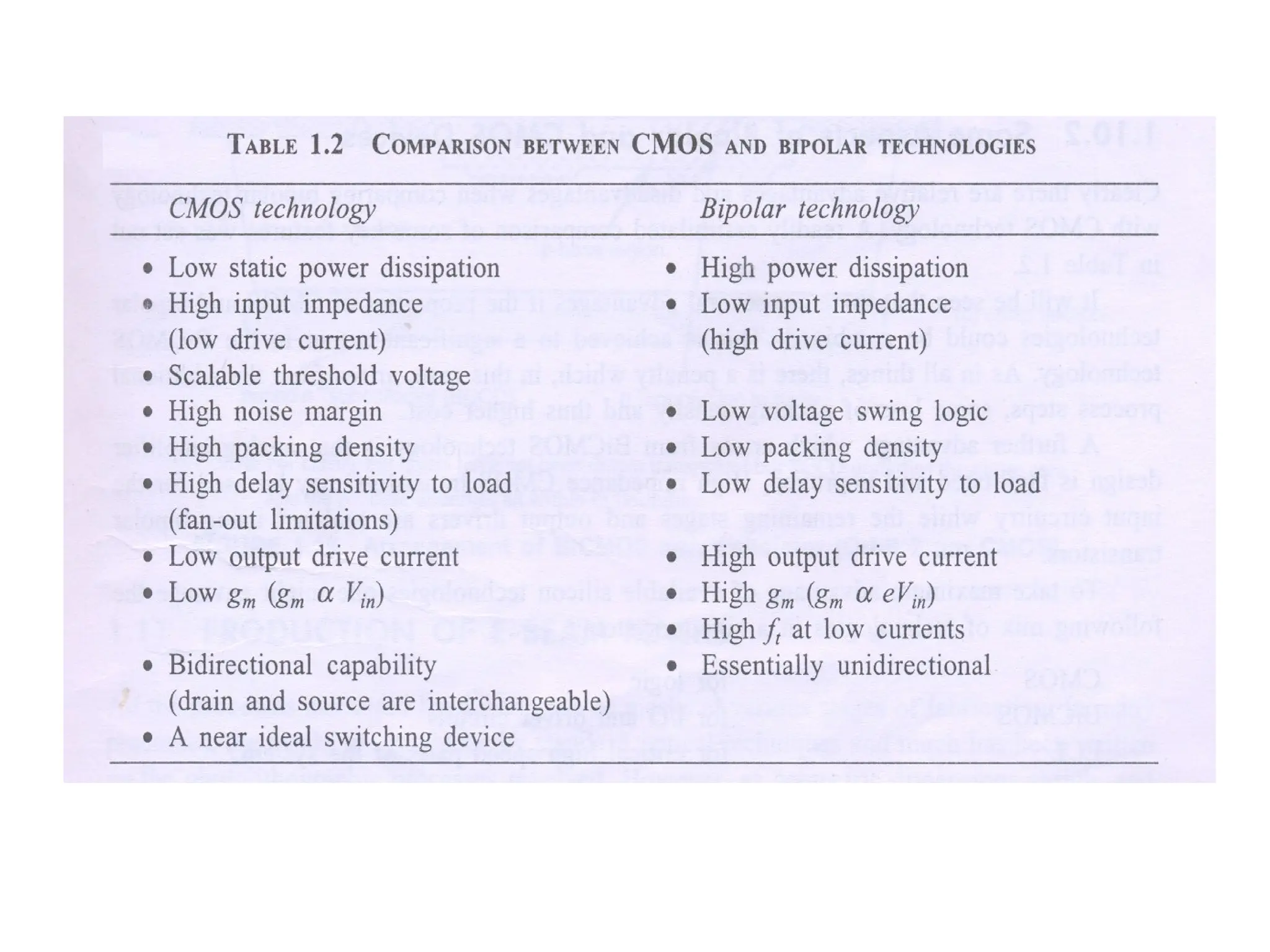
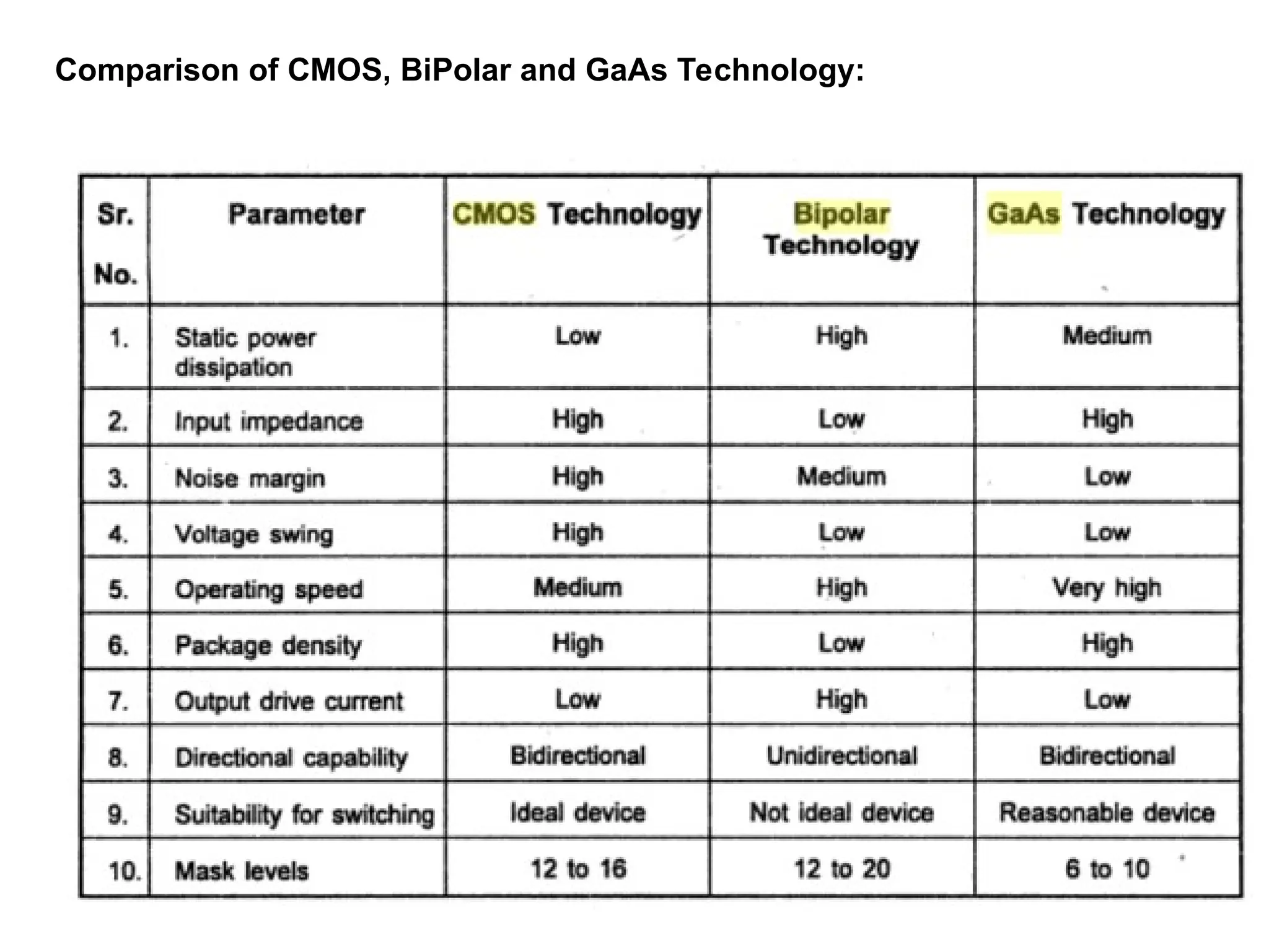
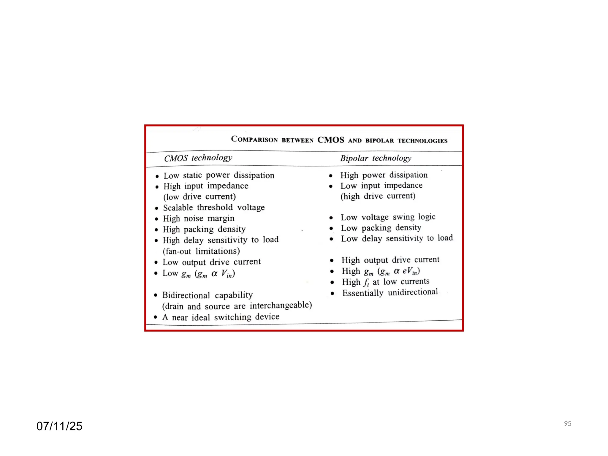
A comparison between the characteristics of CMOS and bipolar circuits is
set out in Table 1.2 and the differences are self-evident. BiCMOS technology goes
some way toward combining the virtues of both technologies.
48.
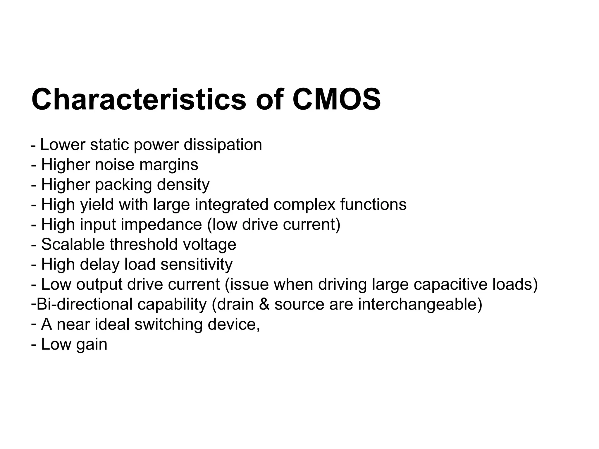
Characteristics of CMOS
-Lower static power dissipation
- Higher noise margins
- Higher packing density
- High yield with large integrated complex functions
- High input impedance (low drive current)
- Scalable threshold voltage
- High delay load sensitivity
- Low output drive current (issue when driving large capacitive loads)
-Bi-directional capability (drain & source are interchangeable)
- A near ideal switching device,
- Low gain
49.
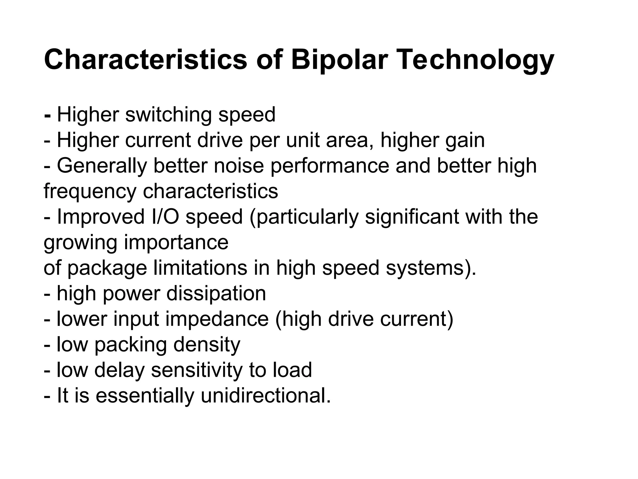
Characteristics of BipolarTechnology
- Higher switching speed
- Higher current drive per unit area, higher gain
- Generally better noise performance and better high
frequency characteristics
- Improved I/O speed (particularly significant with the
growing importance
of package limitations in high speed systems).
- high power dissipation
- lower input impedance (high drive current)
- low packing density
- low delay sensitivity to load
- It is essentially unidirectional.
52.
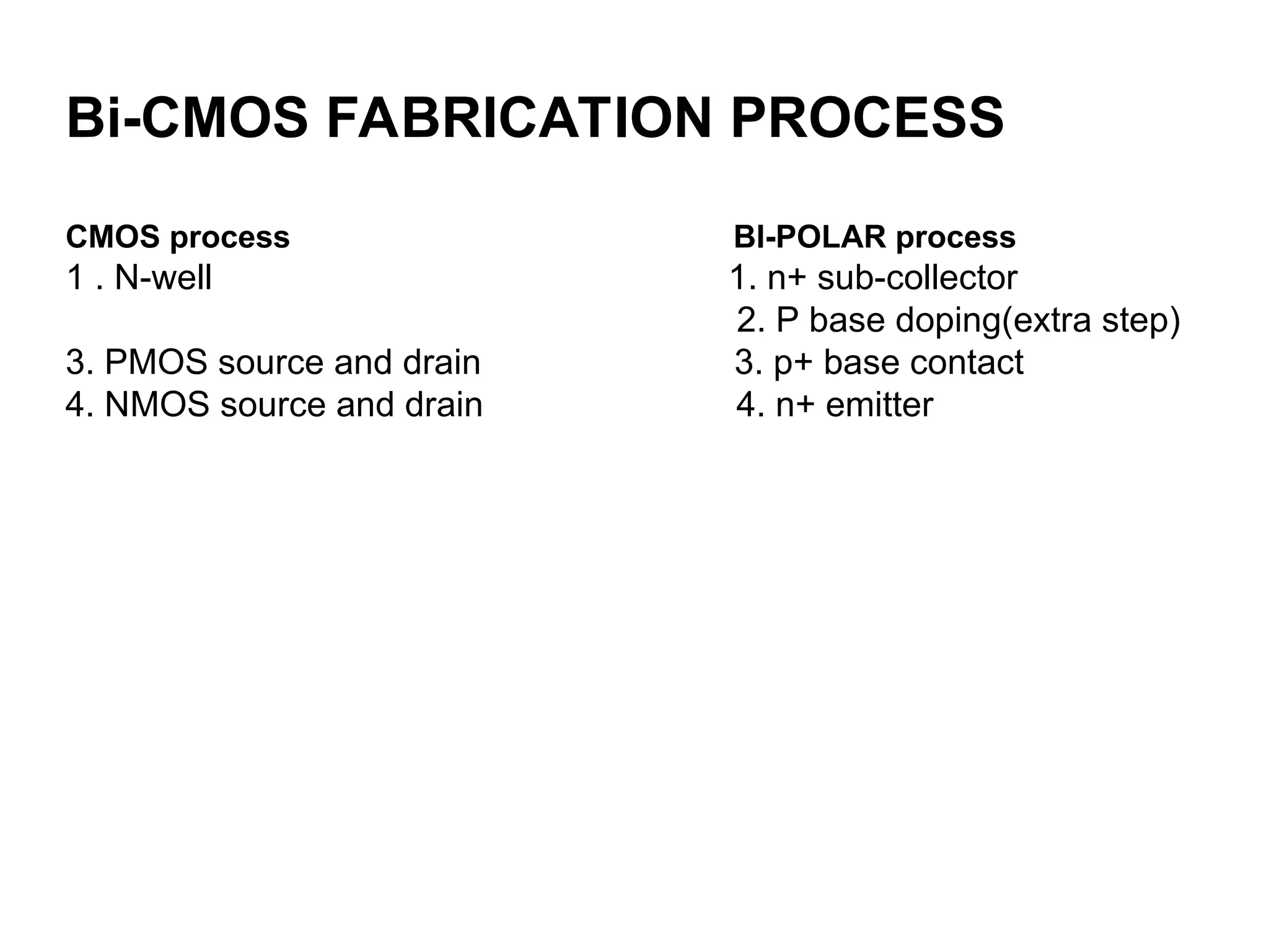
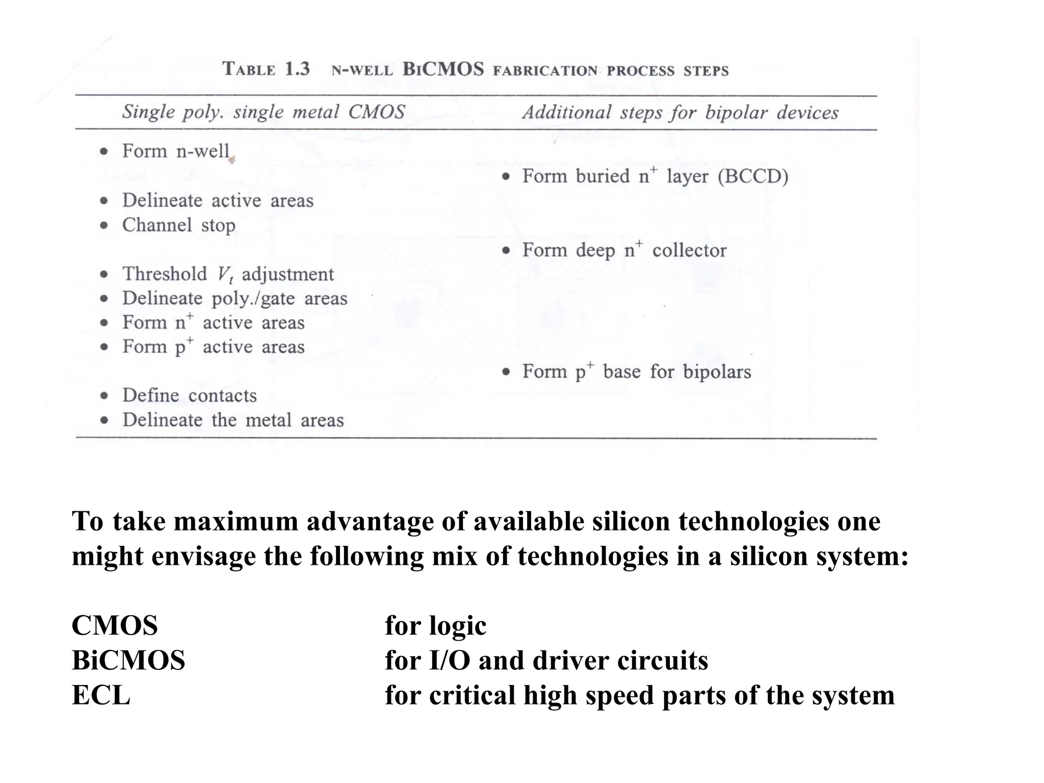
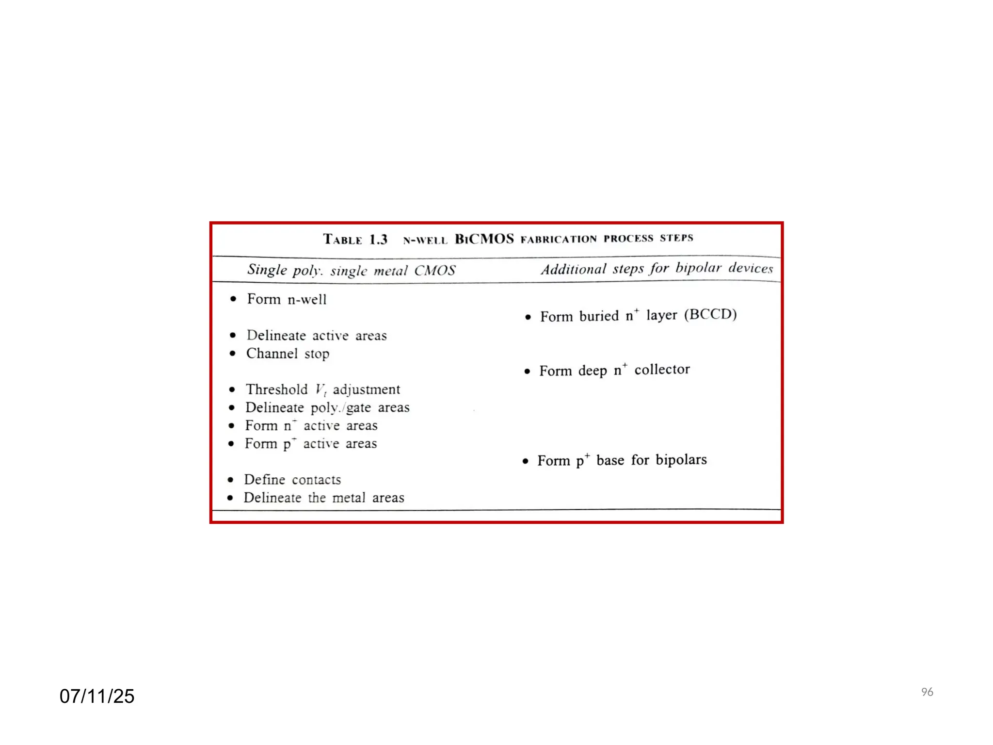
Bi-CMOS FABRICATION PROCESS
CMOSprocess BI-POLAR process
1 . N-well 1. n+ sub-collector
2. P base doping(extra step)
3. PMOS source and drain 3. p+ base contact
4. NMOS source and drain 4. n+ emitter
53.
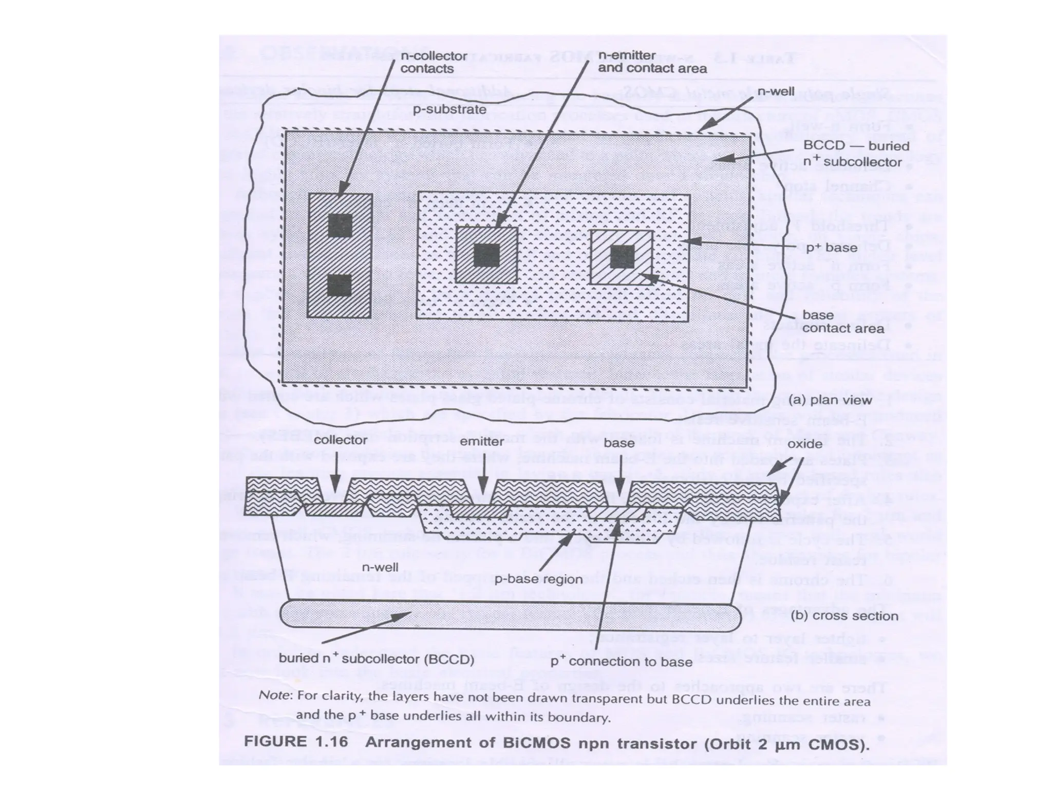
When considering CMOStechnology, it becomes apparent that
theoretically there should be little difficulty in extending the fabrication processes
to include bipolar as well as MOS transistors. Indeed, a problem of p-well and n-
well CMOS processing is that parasitic bipolar transistors are inadvertently formed
as part of the outcome of fabrication.
The production of npn bipolar transistors with good performance
characteristics can be achieved, for example, by extending the standard n-well
CMOS processing to include further masks to add two additional layers- the n+
subcollector and p+ base layers.
The npn transistor is formed in an n-well and the additional p+
base region
is located in the well to form the p-base region of the transistor.
The second additional layer, the buried n+
subcollector (BCCD), is added
to reduce the n-well (collector) resistance and thus improve the quality of the
bipolar transistor. The simplified general arrangement of such a bipolar npn
transistor may be appreciated with regard to Figure 1.16.
54.
To take maximumadvantage of available silicon technologies one
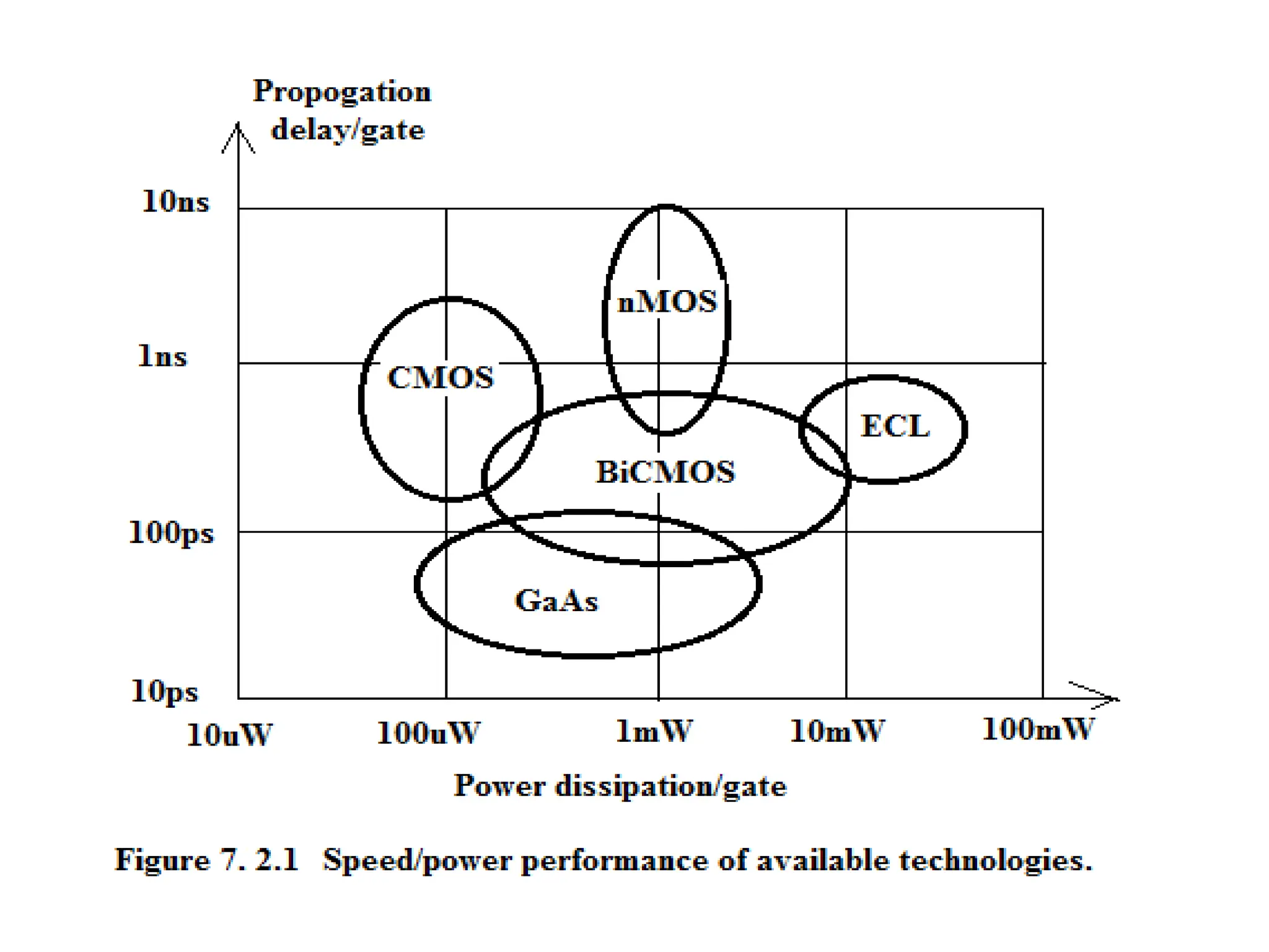
might envisage the following mix of technologies in a silicon system:
CMOS for logic
BiCMOS for I/O and driver circuits
ECL for critical high speed parts of the system
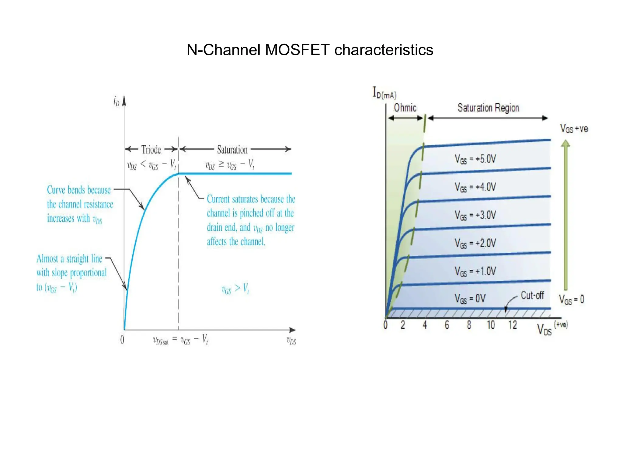
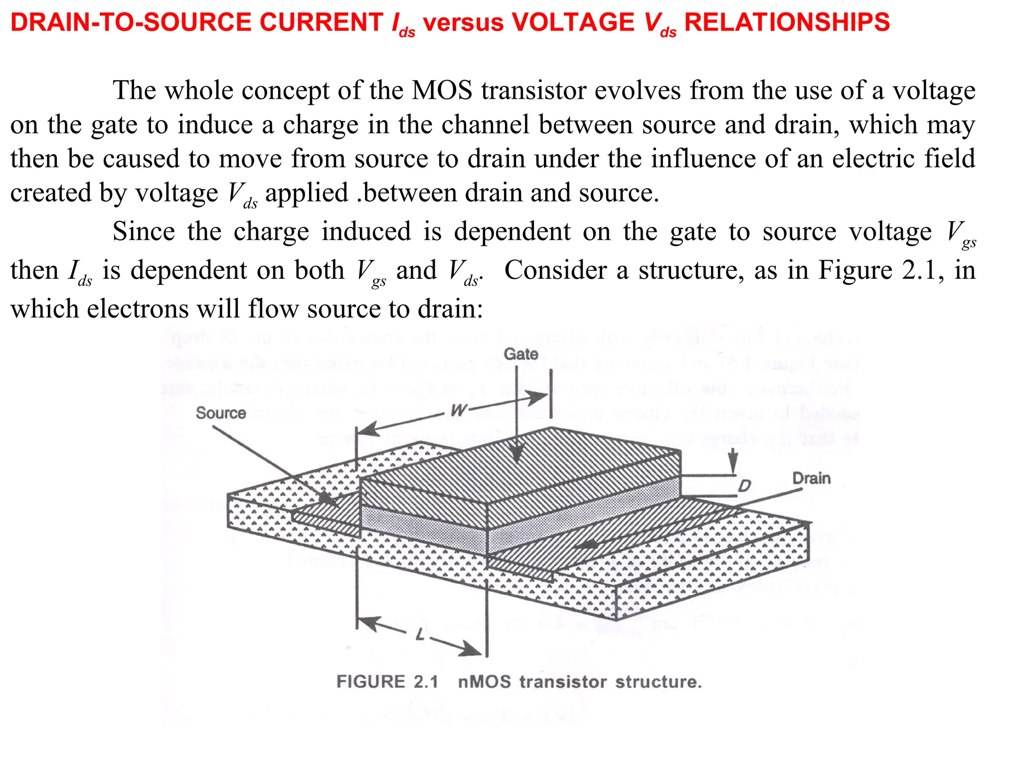
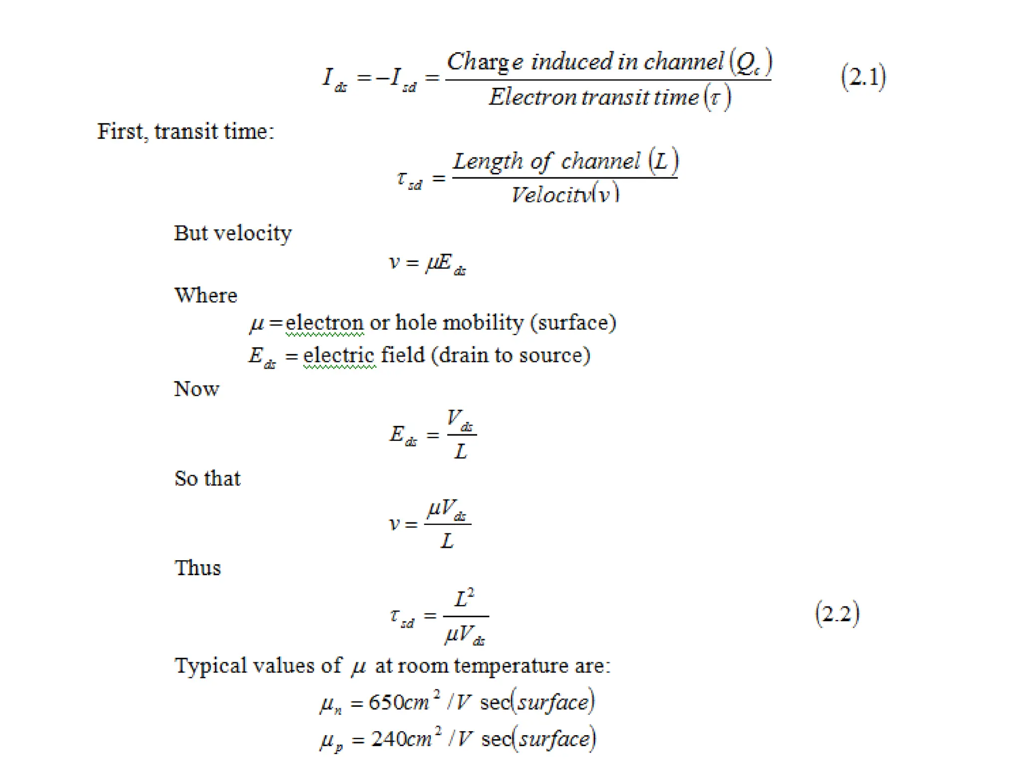
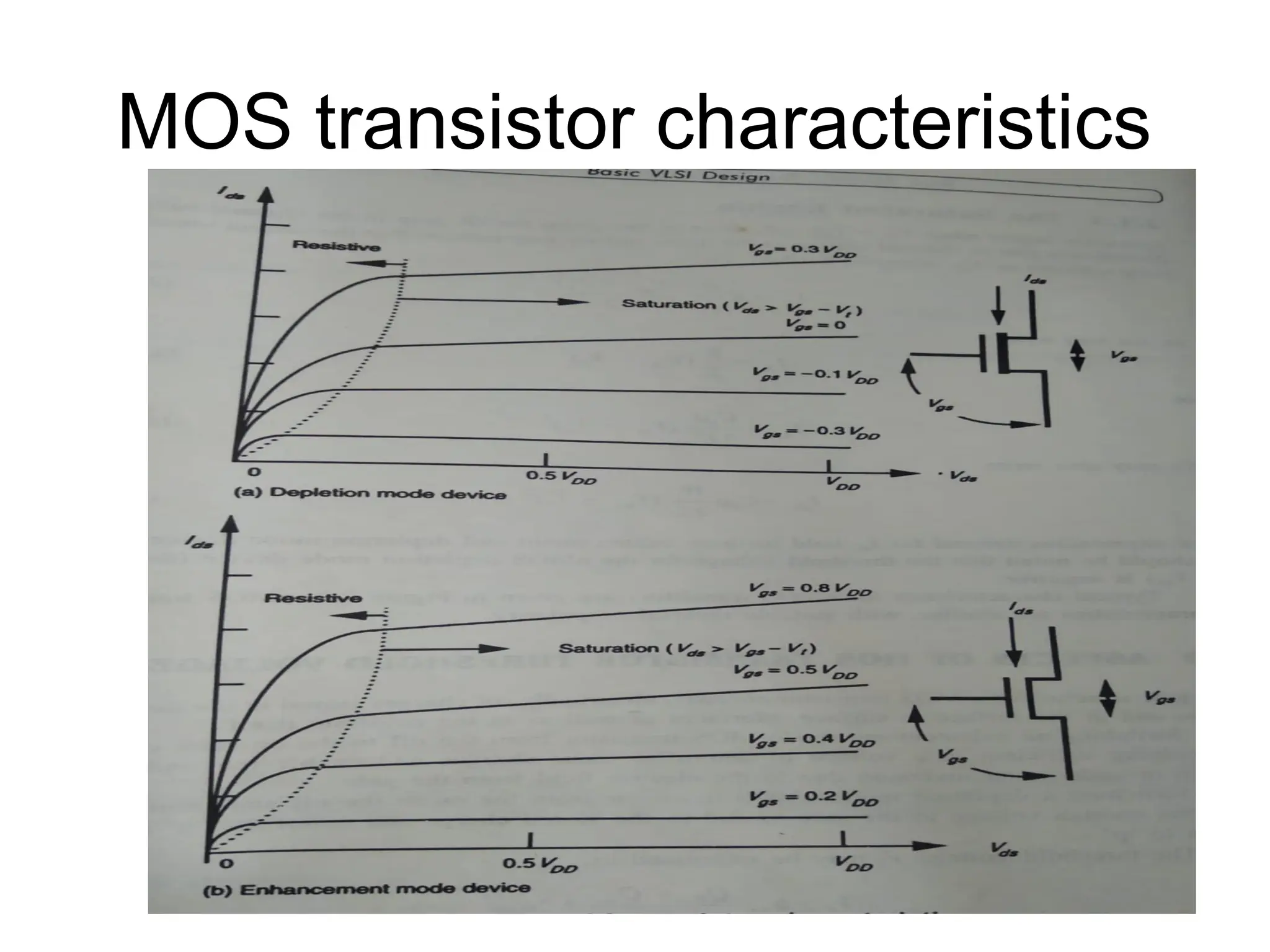
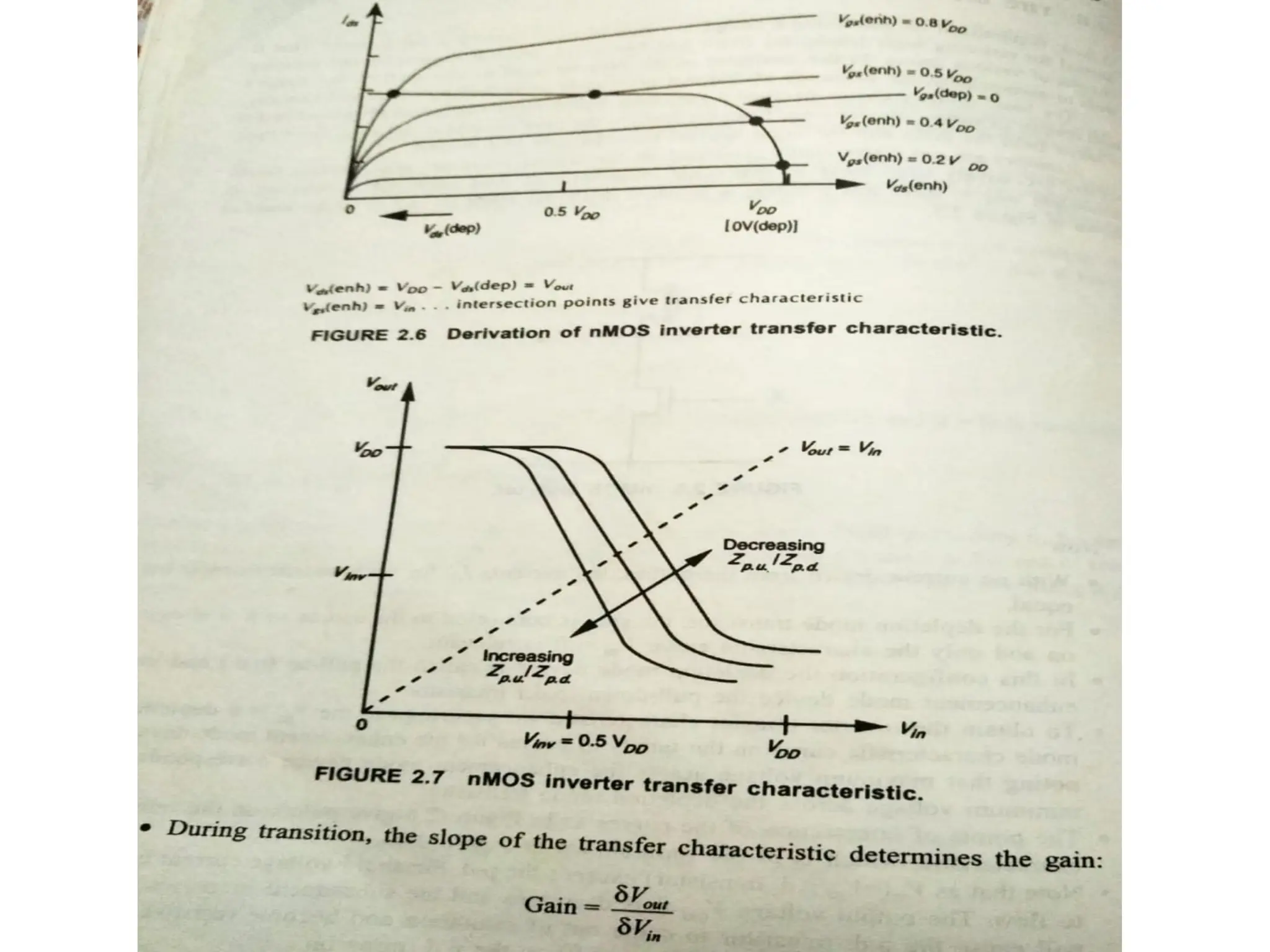
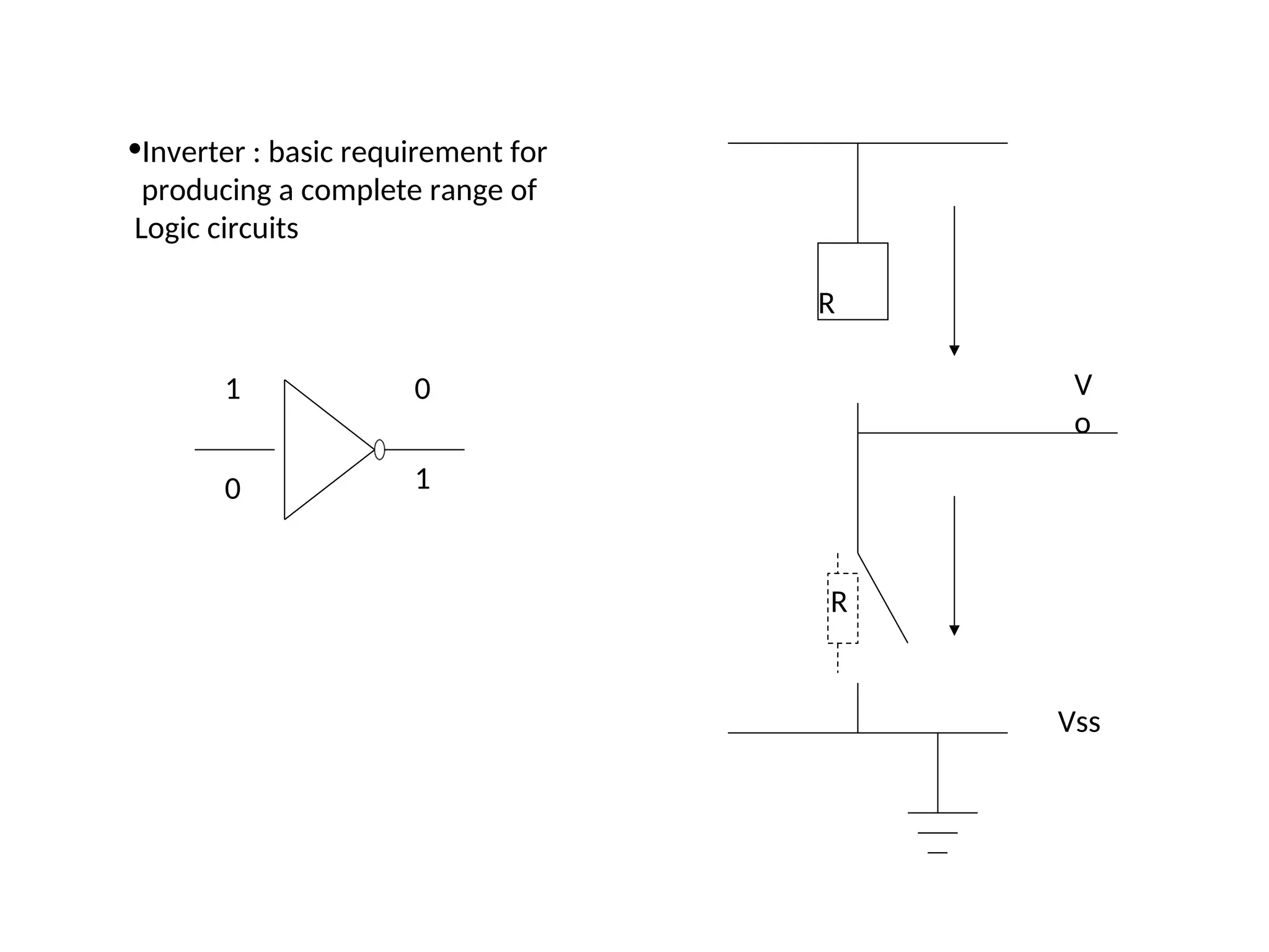
DRAIN-TO-SOURCE CURRENT Idsversus VOLTAGE Vds RELATIONSHIPS
The whole concept of the MOS transistor evolves from the use of a voltage
on the gate to induce a charge in the channel between source and drain, which may
then be caused to move from source to drain under the influence of an electric field
created by voltage Vds applied .between drain and source.
Since the charge induced is dependent on the gate to source voltage Vgs
then Ids is dependent on both Vgs and Vds. Consider a structure, as in Figure 2.1, in
which electrons will flow source to drain:
59.
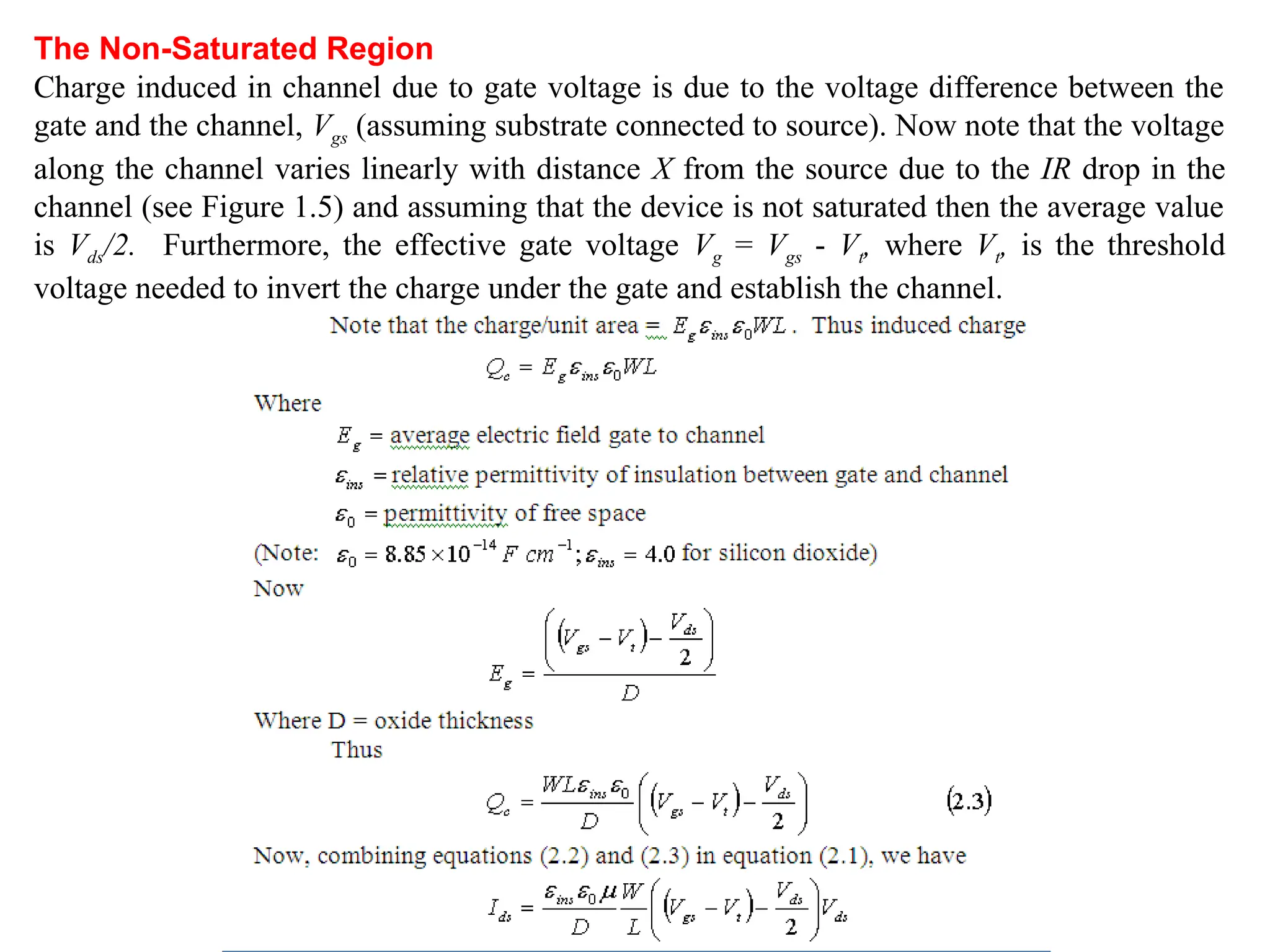
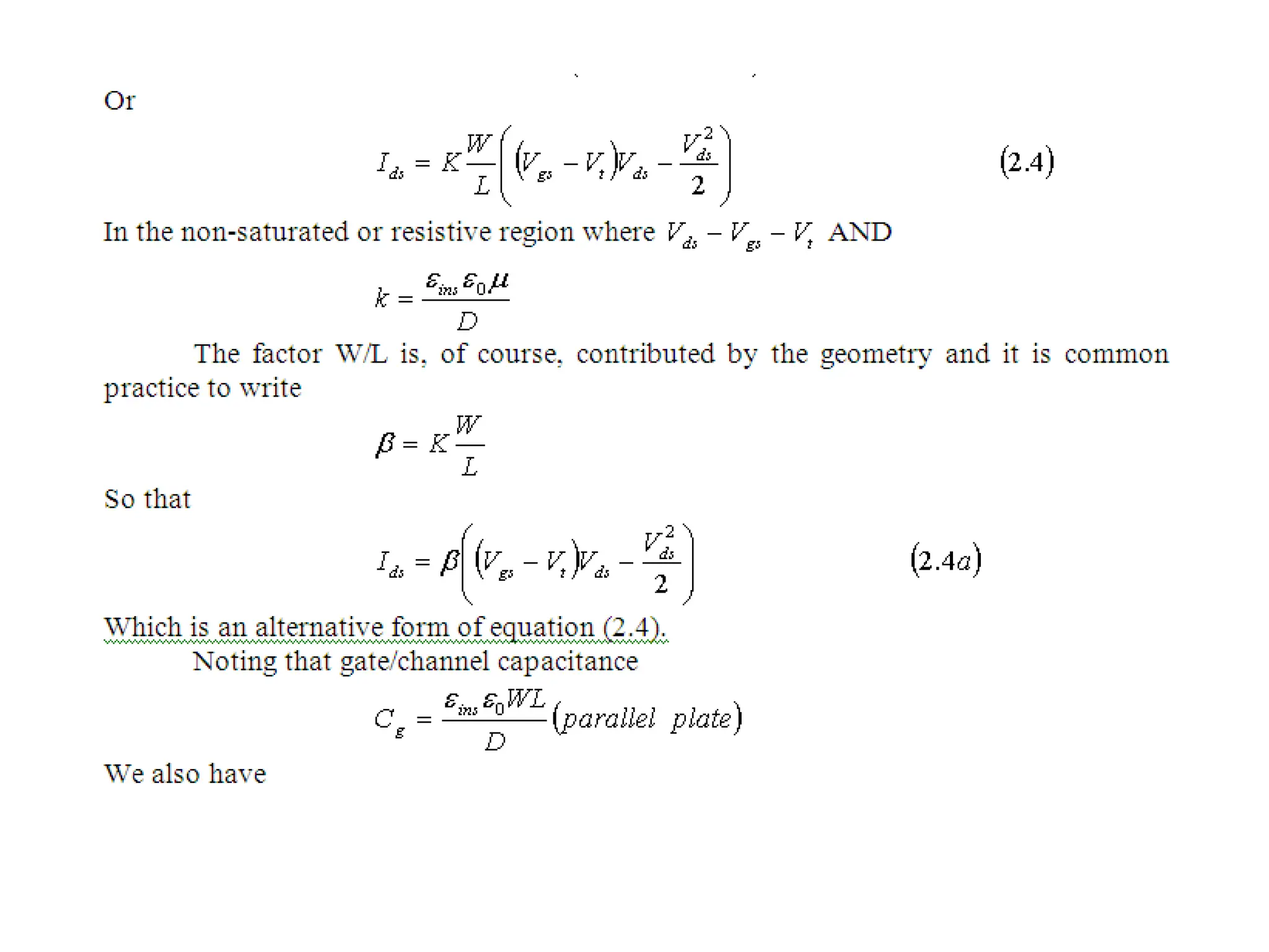
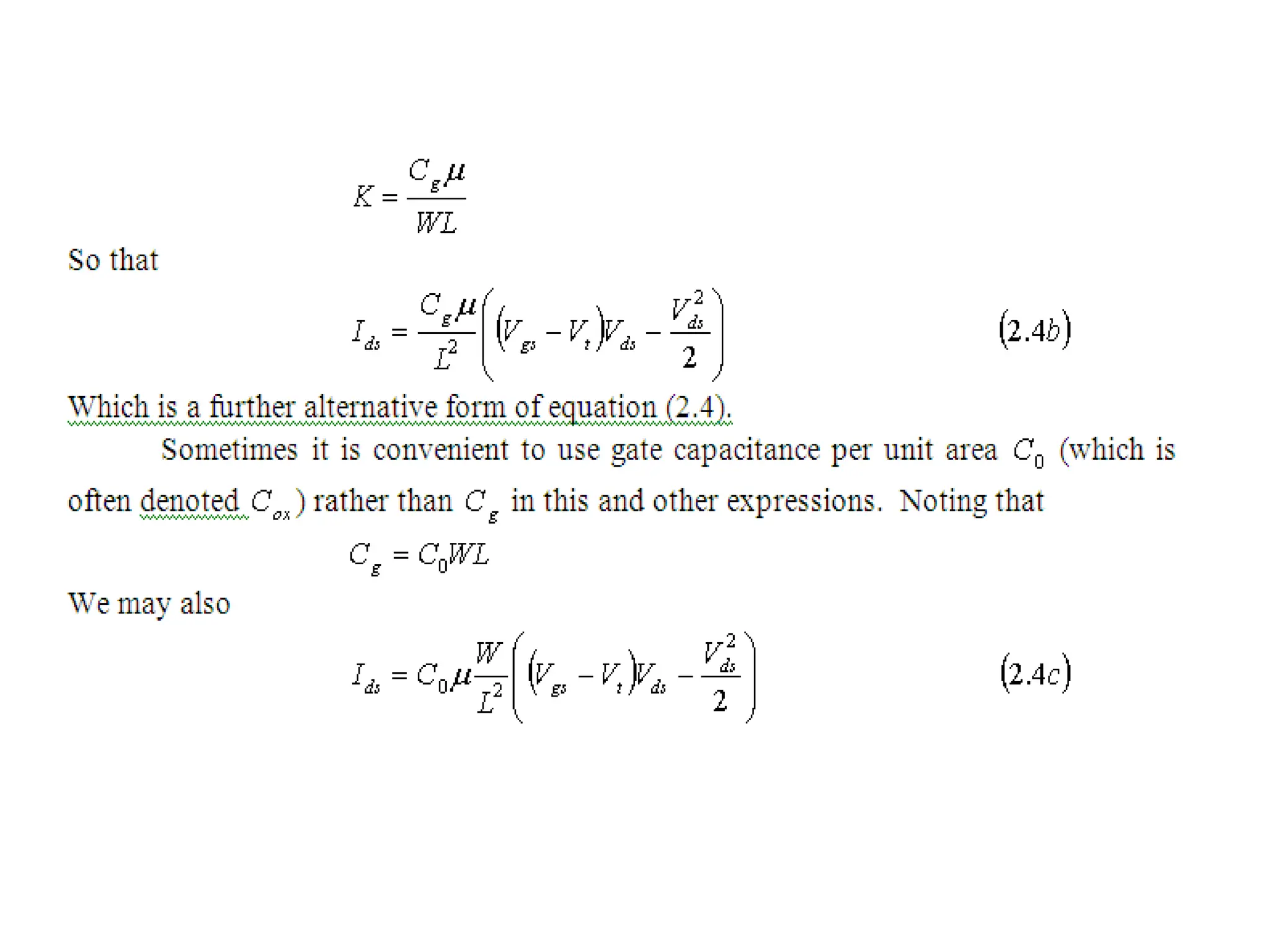
The Non-Saturated Region
Chargeinduced in channel due to gate voltage is due to the voltage difference between the
gate and the channel, Vgs (assuming substrate connected to source). Now note that the voltage
along the channel varies linearly with distance X from the source due to the IR drop in the
channel (see Figure 1.5) and assuming that the device is not saturated then the average value
is Vds/2. Furthermore, the effective gate voltage Vg = Vgs - Vt, where Vt, is the threshold
voltage needed to invert the charge under the gate and establish the channel.
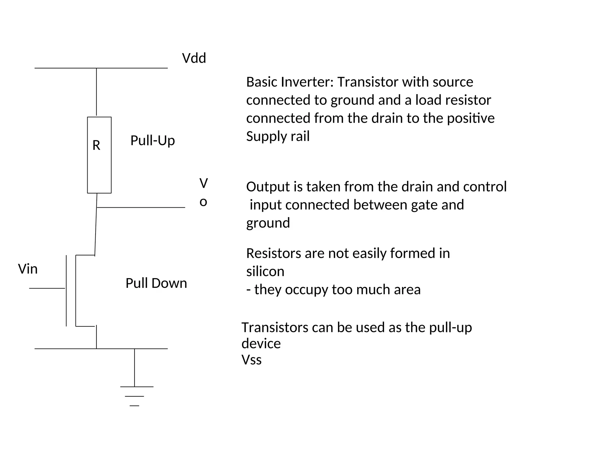
Vdd
V
o
Vin
R Pull-Up
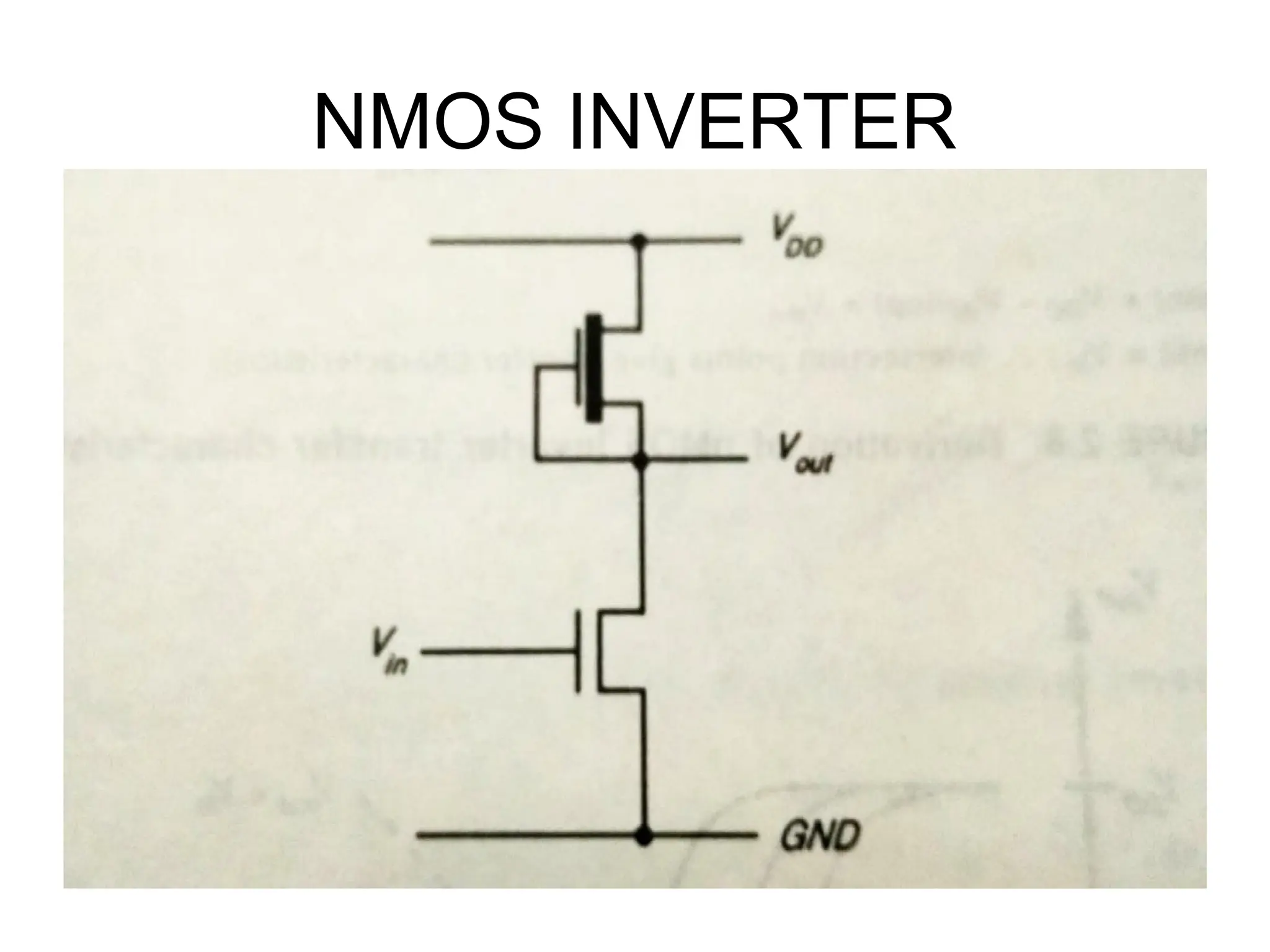
Pull Down
BasicInverter: Transistor with source
connected to ground and a load resistor
connected from the drain to the positive
Supply rail
Output is taken from the drain and control
input connected between gate and
ground
Resistors are not easily formed in
silicon
- they occupy too much area
Transistors can be used as the pull-up
device
Vss
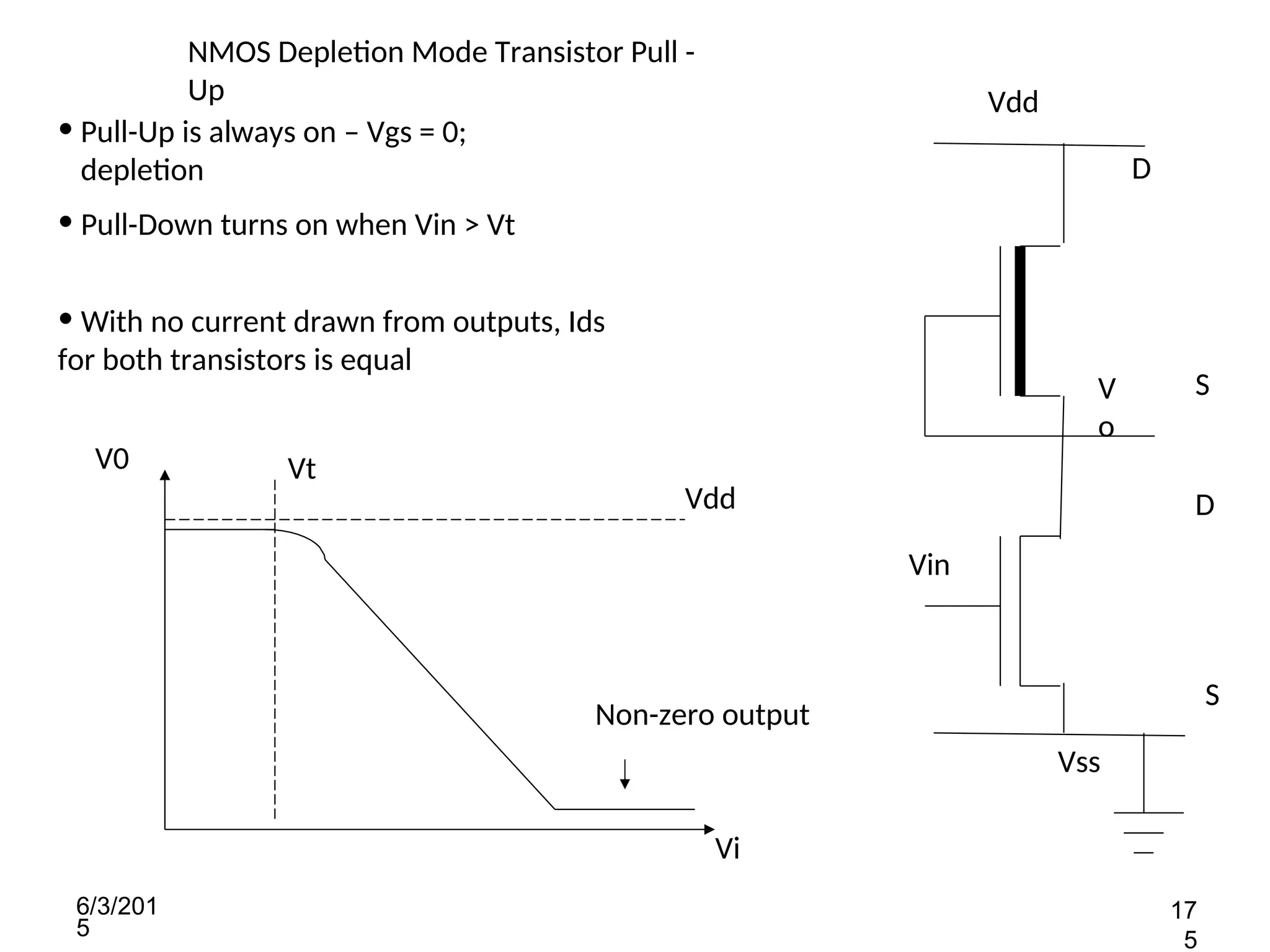
69.
Vdd
Vss
V
o
Vin
D
S
D
S
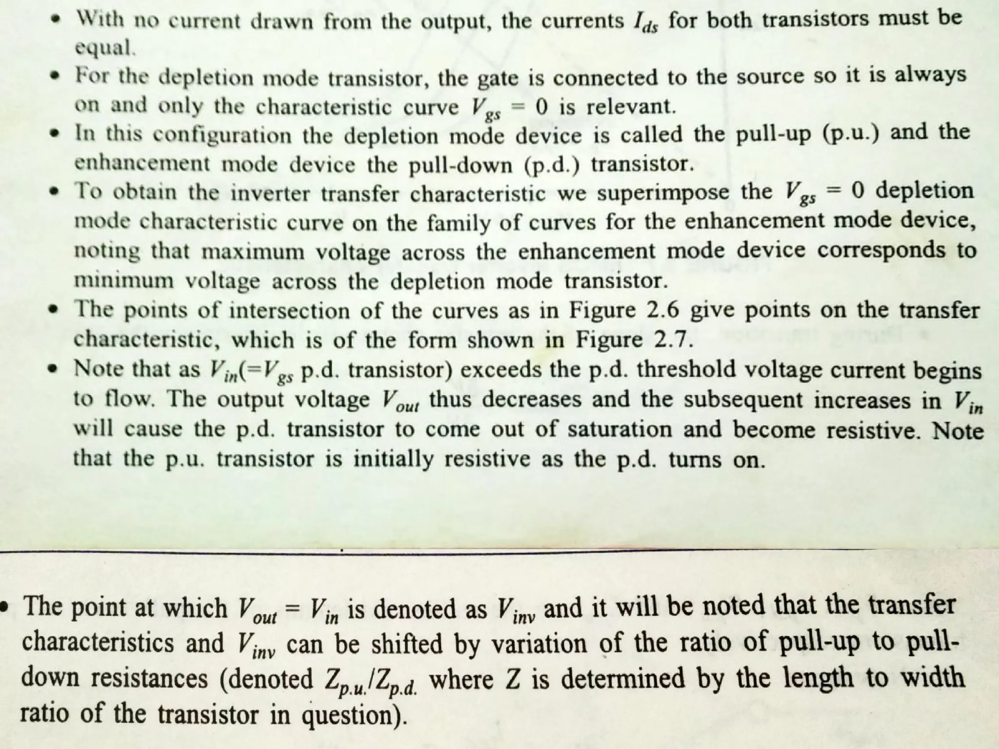
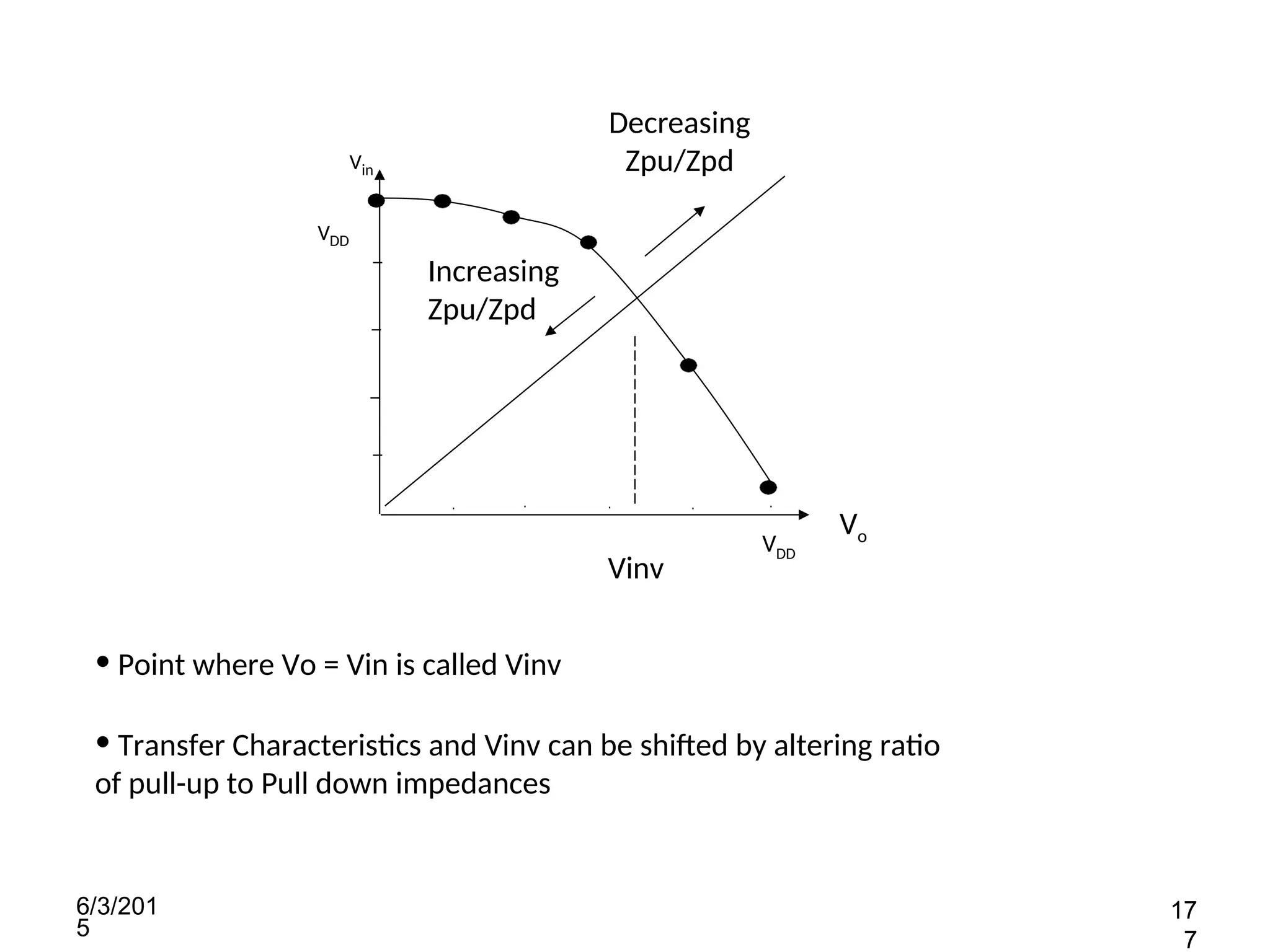
• Pull-Up isalways on – Vgs = 0;
depletion
• Pull-Down turns on when Vin > Vt
NMOS Depletion Mode Transistor Pull -
Up
Vt
V0
Vdd
Vi
• With no current drawn from outputs, Ids
for both transistors is equal
6/3/201
5
17
5
Non-zero output
6/3/201
5
17
8
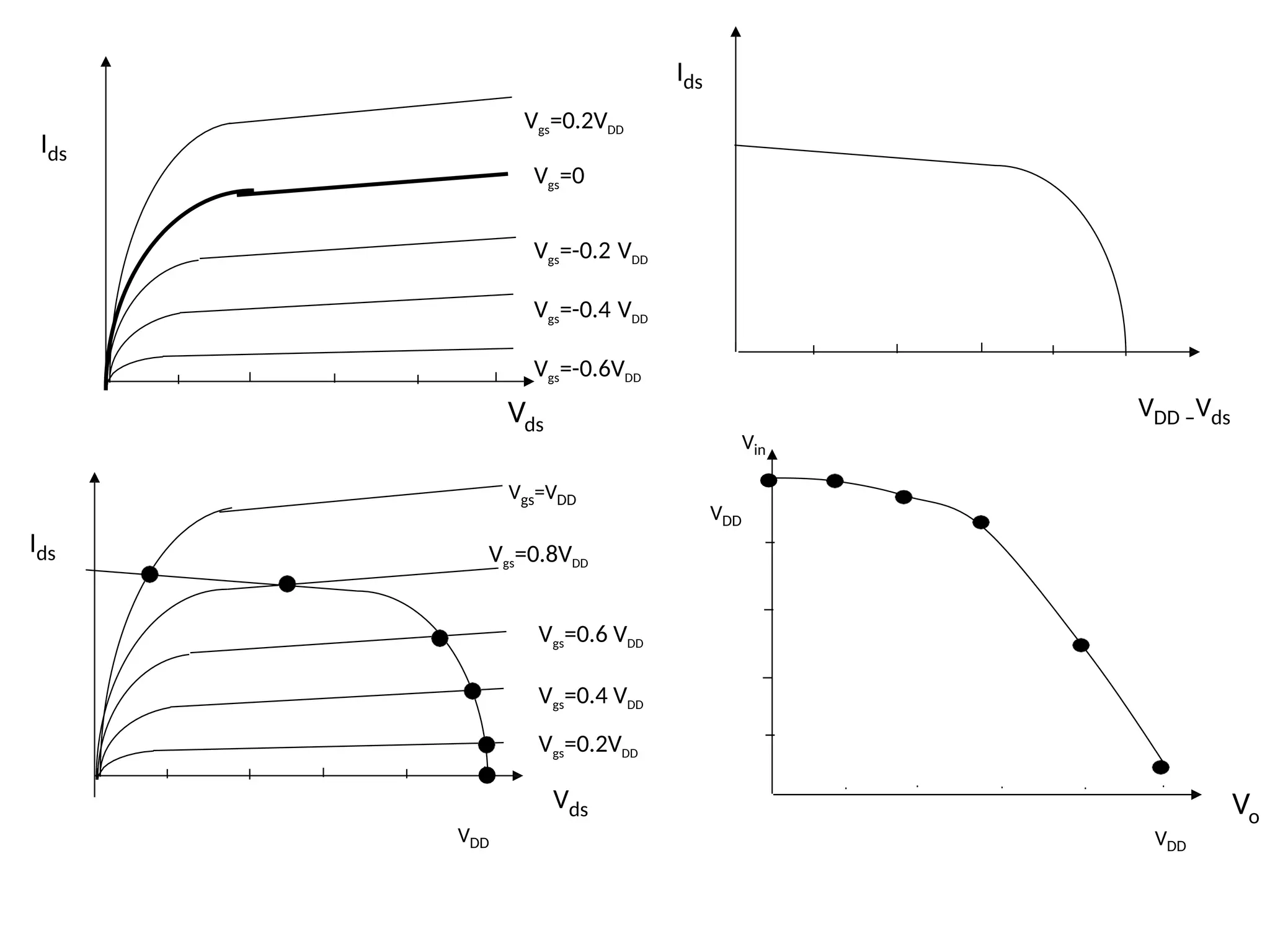
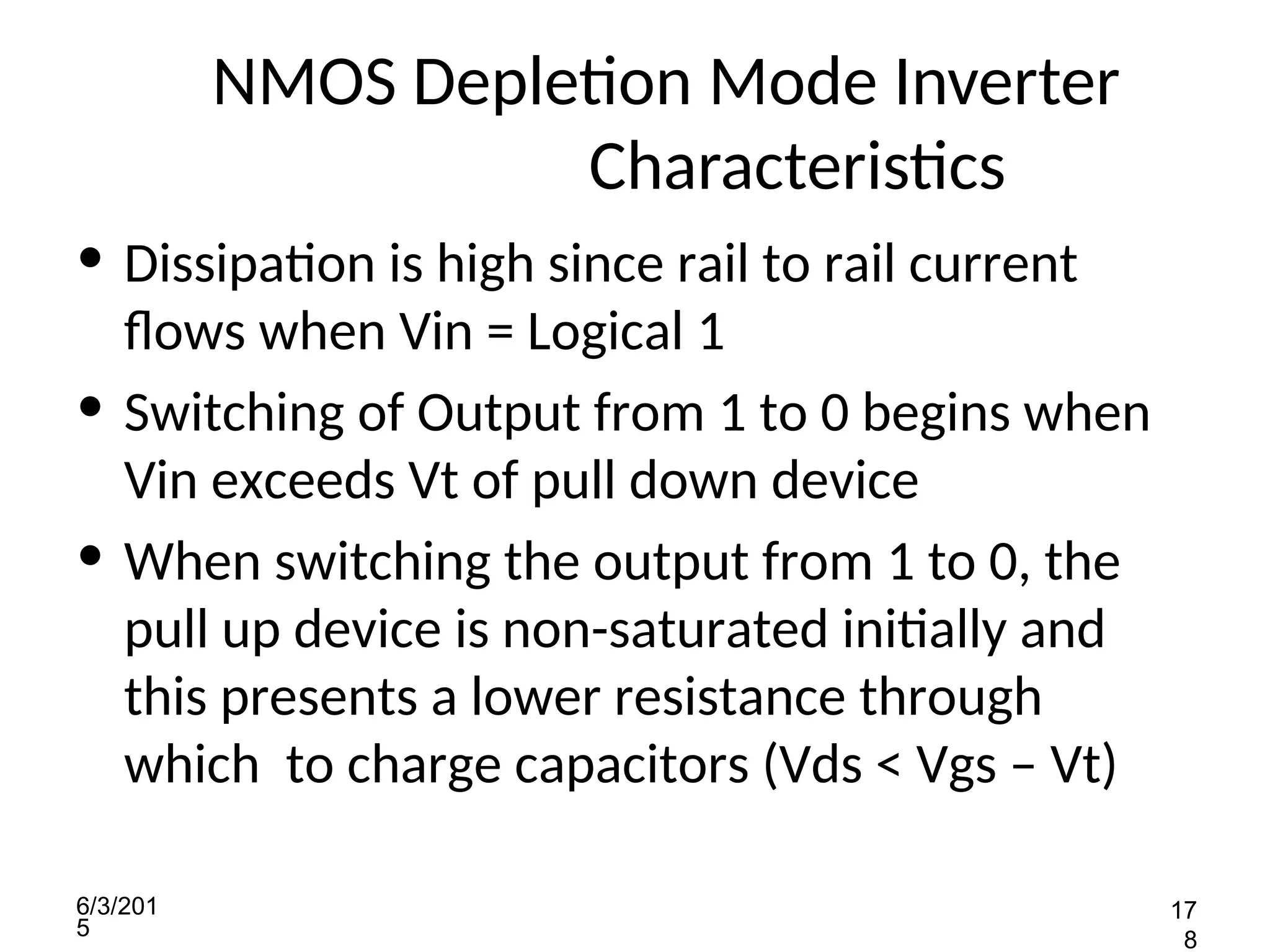
NMOS Depletion ModeInverter
Characteristics
• Dissipation is high since rail to rail current
flows when Vin = Logical 1
• Switching of Output from 1 to 0 begins when
Vin exceeds Vt of pull down device
• When switching the output from 1 to 0, the
pull up device is non-saturated initially and
this presents a lower resistance through
which to charge capacitors (Vds < Vgs – Vt)
73.
Vss
V
o
Vin
D
S
D
S
NMOS Enhancement ModeTransistor Pull -
Up
Vdd
Vgg
Vt (pull down)
V0
Vdd
Vt (pull up)
6/3/201
5
17
9
Non zero output
Vin
• Dissipation is high since current flows when Vin = 1
• Vout can never reach Vdd (effect of
channel)
•Vgg can be derived from a switching source (i.e. one phase
of a clock, so that dissipation can be significantly reduced
• If Vgg is higher than Vdd, and extra supply rail is
required
74.
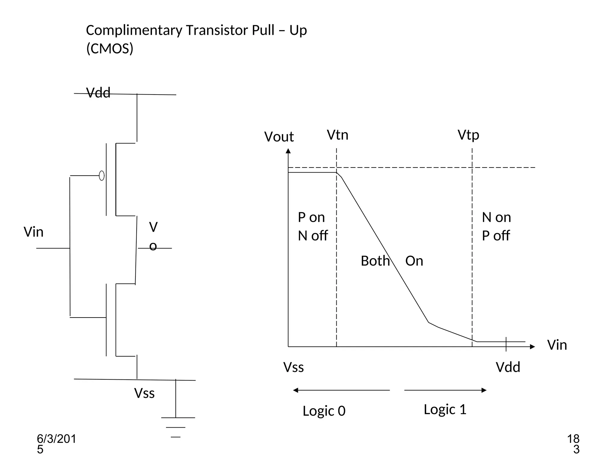
Complimentary Transistor Pull– Up
(CMOS)
Vdd
Vss
V
o
Vin
Vout
Vin
Vdd
Vss
Vtn Vtp
Logic 0
6/3/201
5
18
3
Logic 1
P on
N off
Both On
N on
P off
75.
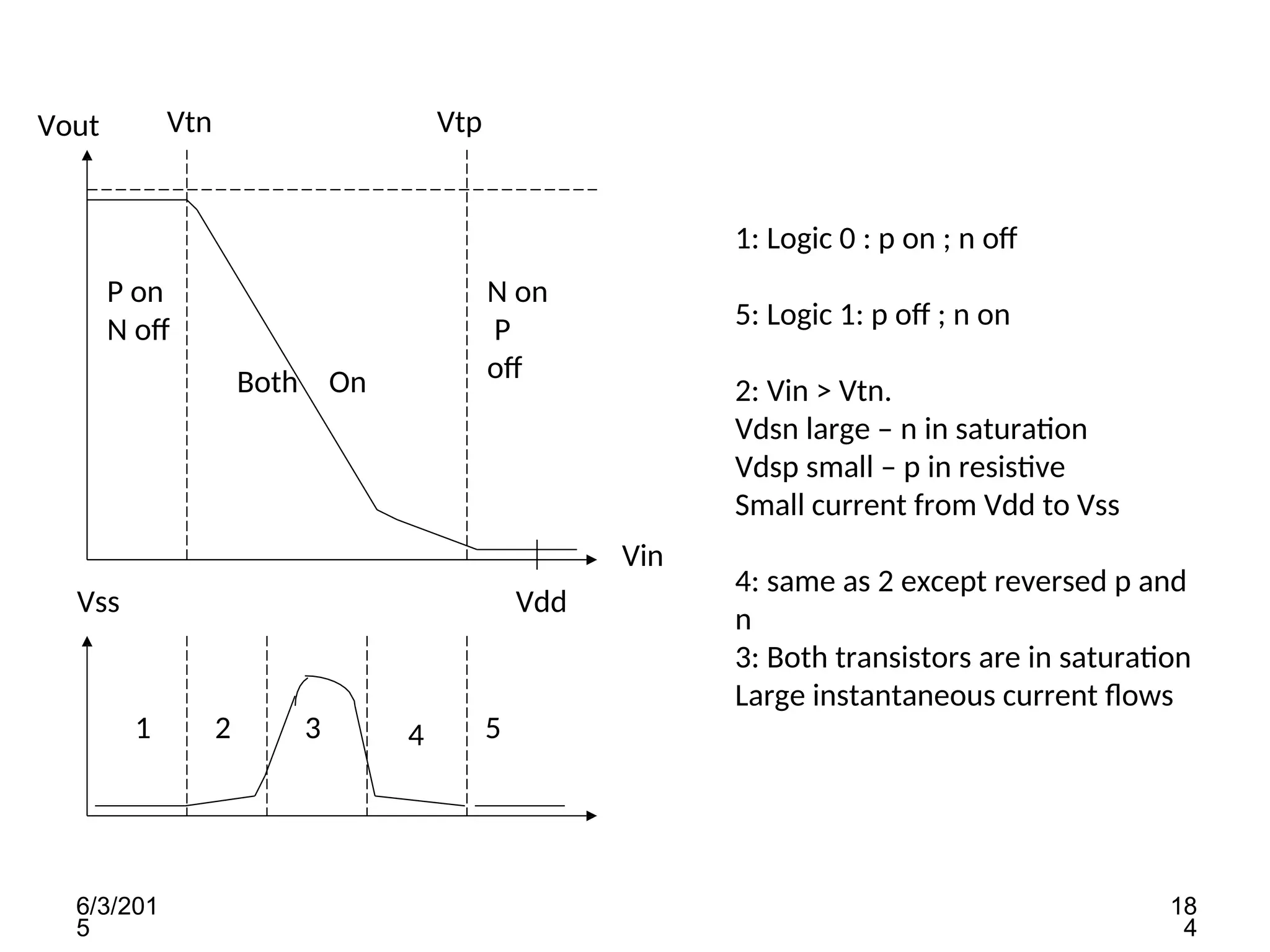
Vout
Vin
Vdd
Vss
Vtn Vtp
P on
Noff
Both On
N on
P
off
1 2 3 4 5
1: Logic 0 : p on ; n off
6/3/201
5
18
4
5: Logic 1: p off ; n on
2: Vin > Vtn.
Vdsn large – n in saturation
Vdsp small – p in resistive
Small current from Vdd to Vss
4: same as 2 except reversed p and
n
3: Both transistors are in saturation
Large instantaneous current flows
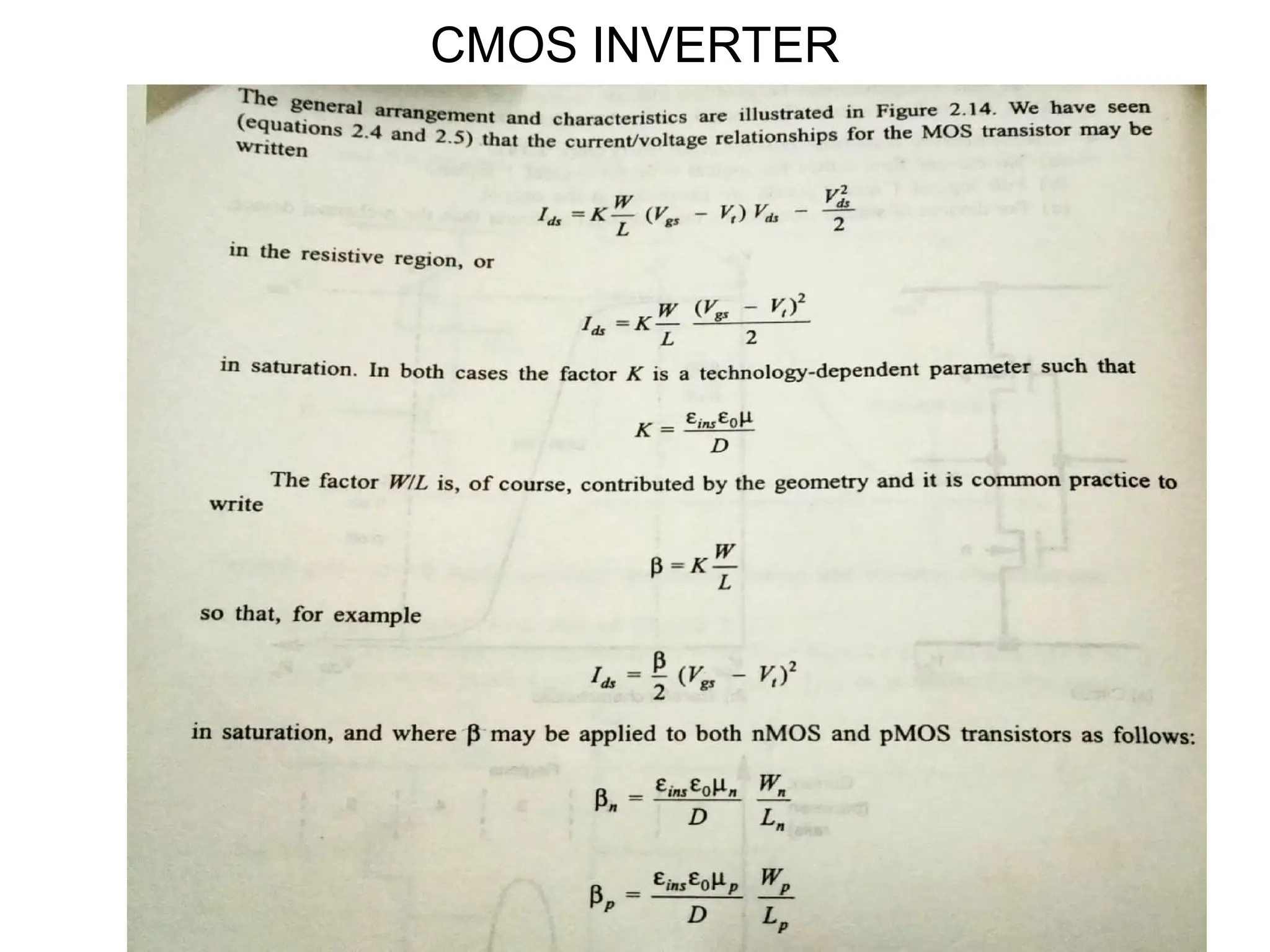
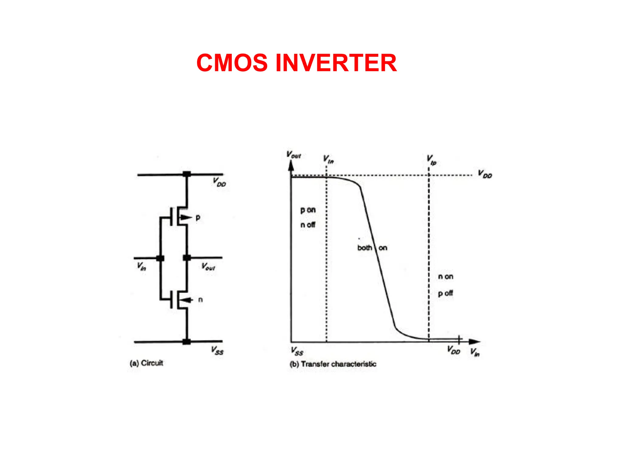
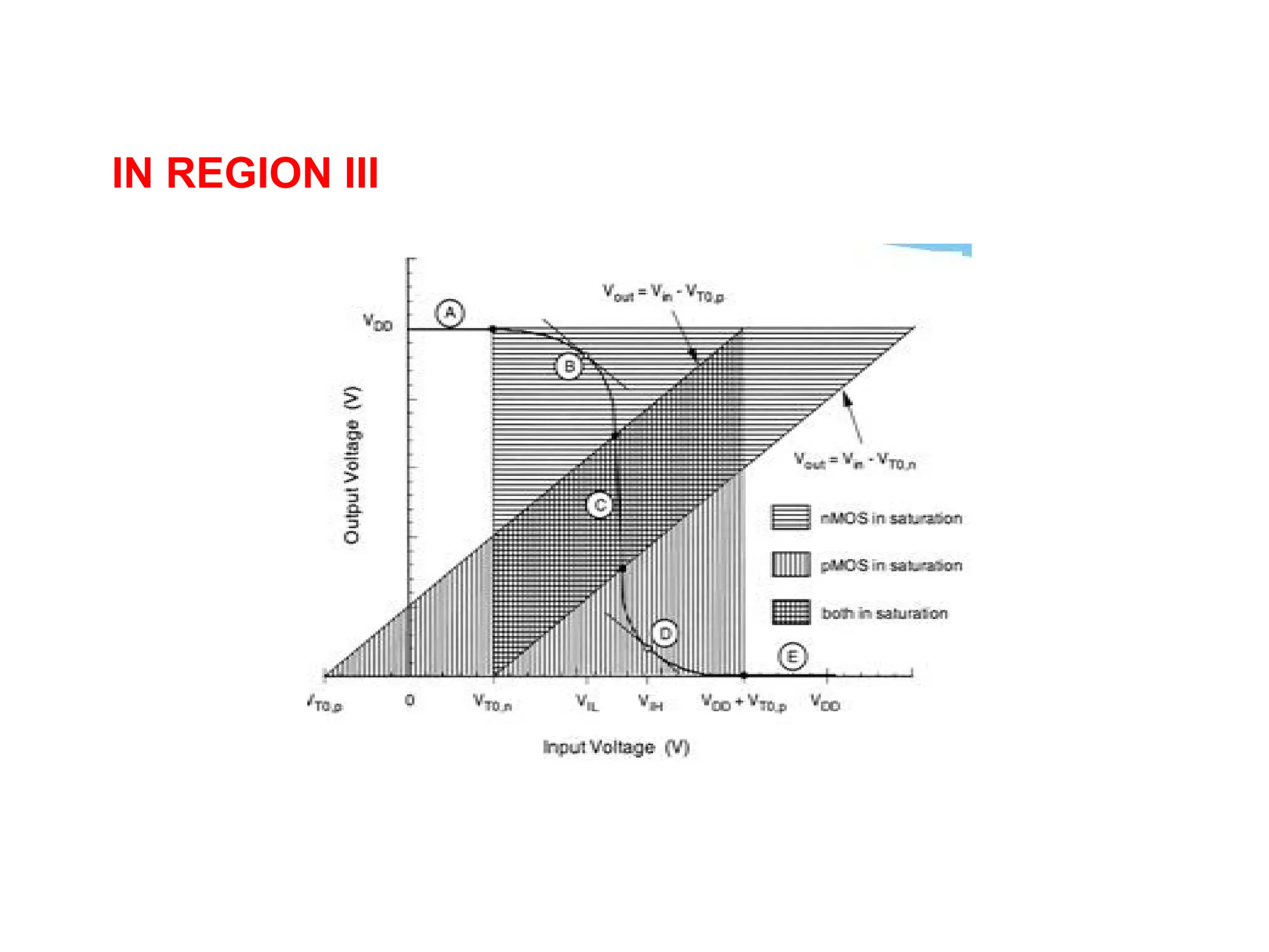
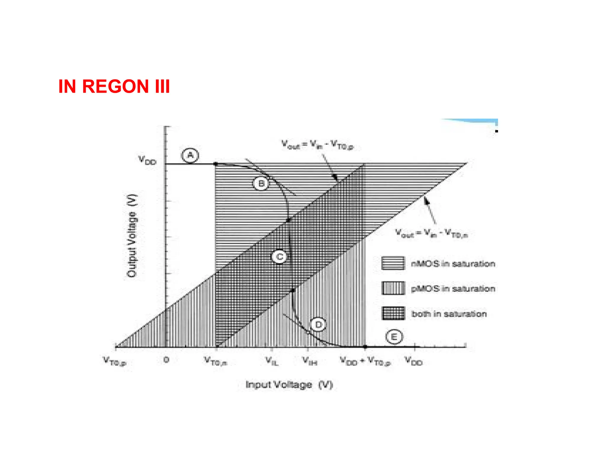
CMOS INVERTER CHARACTERISTICS
Currentthrough n-channel pull-down transistor
2
2
in tn
n
n V V
I
Current through p-channel pull-up transistor
2
2
p
Vtp
Vin VDD
I p
At logic threshold, In = Ip
p
n
tp
in
DD
p
in tn
n
p
n
Vin VDD Vtp
Vin Vtn
Vtn VDD Vtp
Vin VDD
Vtp
Vin Vtn
V V V
V V
n
p
p
n
Vin
1
2
2
2
2
2
2
in
n
n
p
VDD Vtp Vtn
V
1
p
If n = p
and Vtp =
–Vtn
2
VDD
Vin
pWp
nWn
Lp Ln
Mobilities are unequal : µn = 2.5 µp
Z = L/W
pu pd
Z /Z = 2.5:1 for a symmetrical CMOS
inverter
78.
6/3/201
5
18
6
CMOS Inverter Characteristics
•No current flow for either logical 1 or logical
0 inputs
• Full logical 1 and 0 levels are presented at the
output
• For devices of similar dimensions the p –
channel is slower than the n – channel device
79.
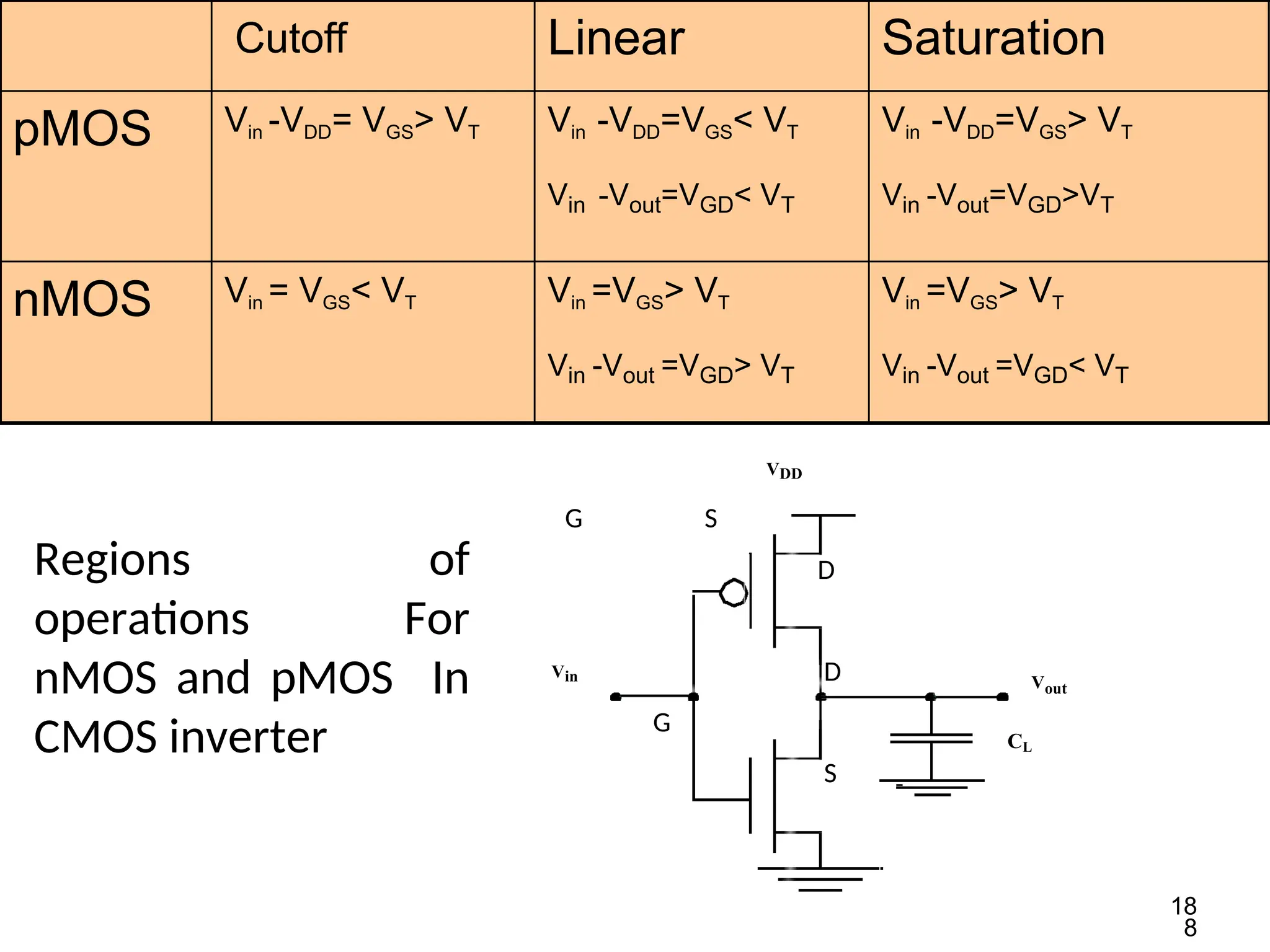
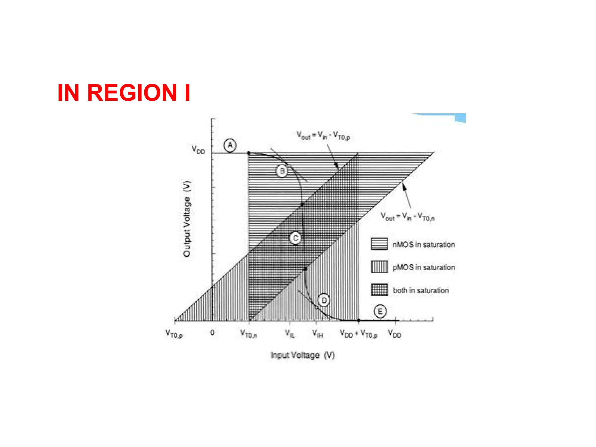
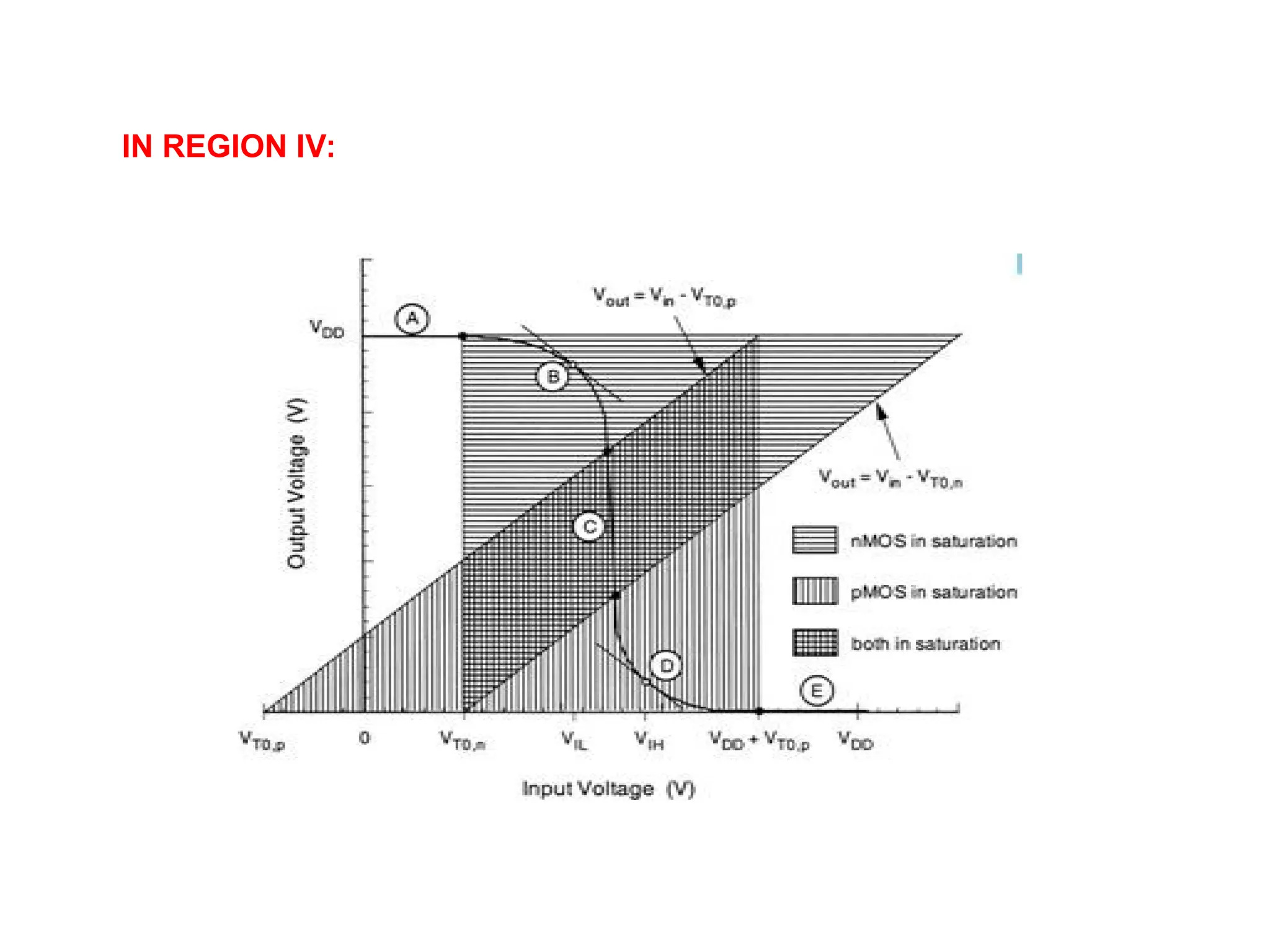
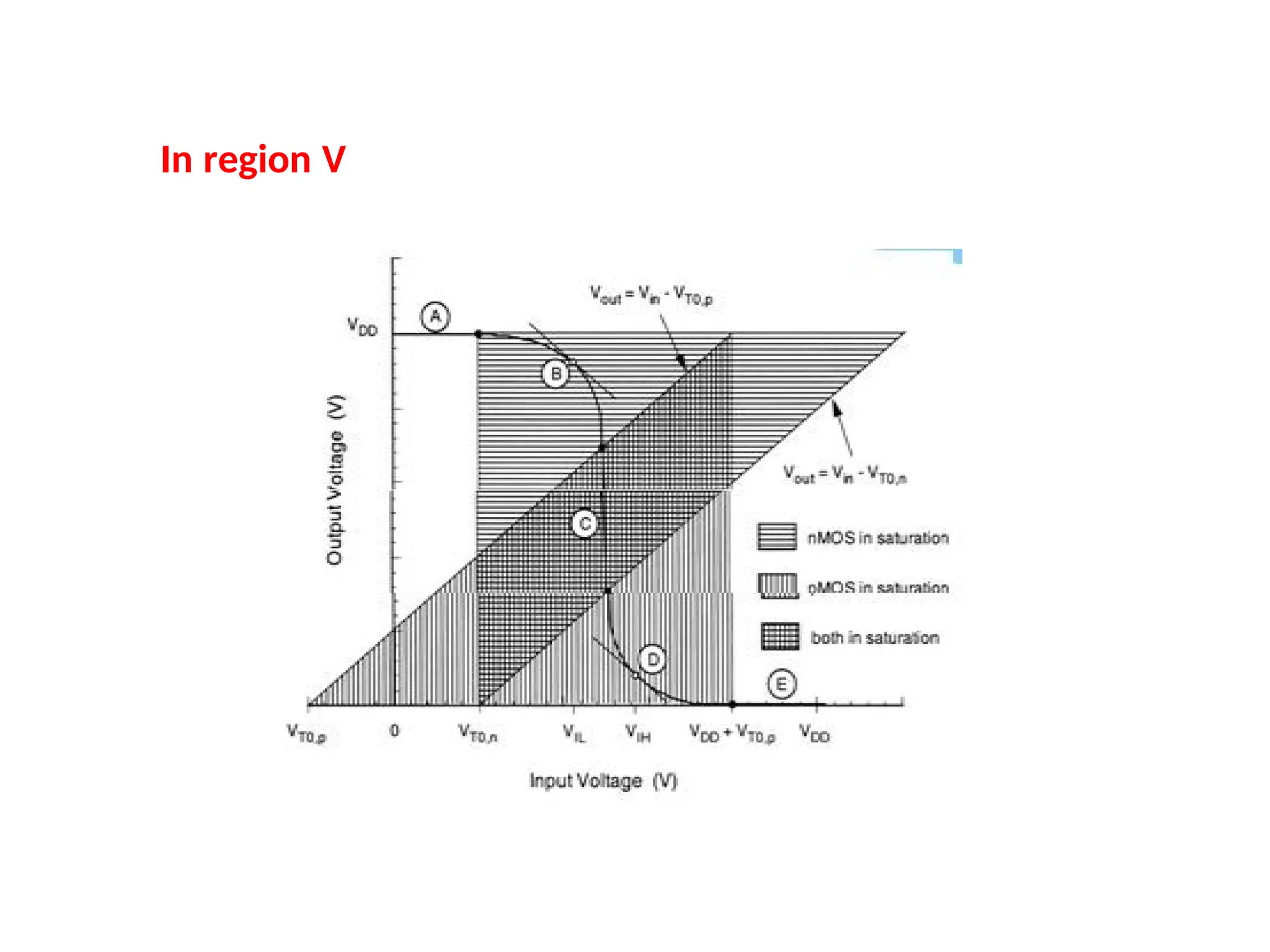
Cutoff Linear Saturation
pMOSVin -VDD= VGS> VT Vin -VDD=VGS< VT
Vin -Vout=VGD< VT
Vin -VDD=VGS> VT
Vin -Vout=VGD>VT
nMOS Vin = VGS< VT Vin =VGS> VT
Vin -Vout =VGD> VT
Vin =VGS> VT
Vin -Vout =VGD< VT
VDD
Vin
18
8
Vout
CL
G S
D
D
G
S
Regions of
operations For
nMOS and pMOS In
CMOS inverter
93
BiCMOS TECHNOLOGY FABRICATION
TheMOS technology lies in the limited load driving capabilities of MOS transistors. This is
due to the limited current sourcing and current sinking abilities associated with both p- and n-
transistors.
Bipolar transistors provide higher gain and have generally better noise and high frequency
characteristics than MOS transistors and have effective way of speeding up VLSI circuits.
When considering CMOS technology, there is difficulty in extending the fabrication
processes to include bipolar as well as MOS transistors.
Indeed, a problem of p-well and n-well CMOS processing is that parasitic bipolar
transistors are formed as part of the outcome of fabrication.
94.
07/11/25 94
The productionof npn bipolar transistors with good performance characteristics can be
achieved by extending the standard n-well CMOS processing to include further masks to
add two additional layers such as the n+
sub-collector and p+
base layers.
The npn transistors is formed in an n- well and the additional p+
base region is located in
the well to form the p-base region of the transistor.
The second additional layer, the buried n+ sub-collector (BCCD), is added to reduce the
n-well (collector) resistance and thus improve the quality of the bipolar transistor.
07/11/25 97
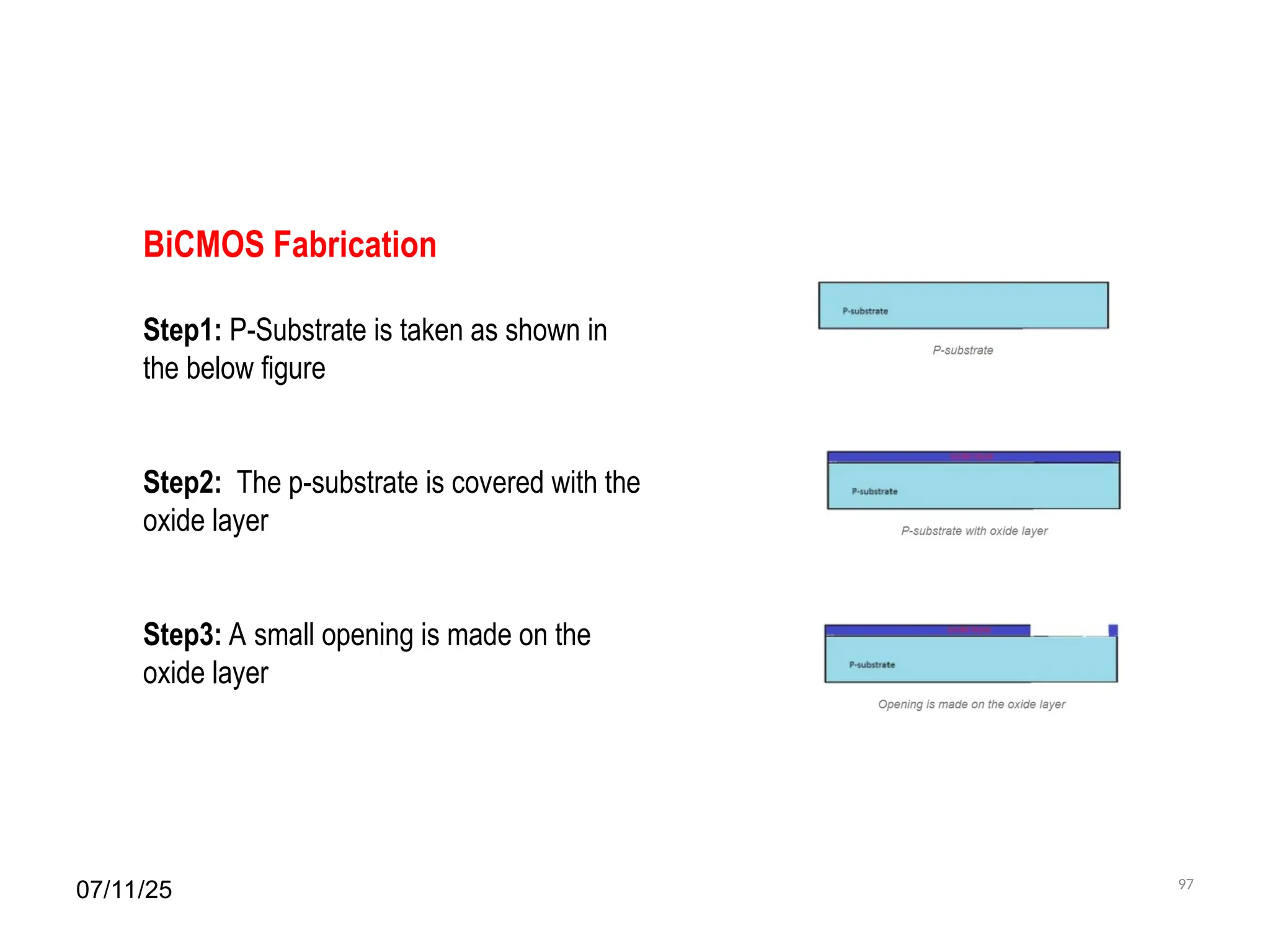
BiCMOS Fabrication
Step1:P-Substrate is taken as shown in
the below figure
Step2: The p-substrate is covered with the
oxide layer
Step3: A small opening is made on the
oxide layer
98.
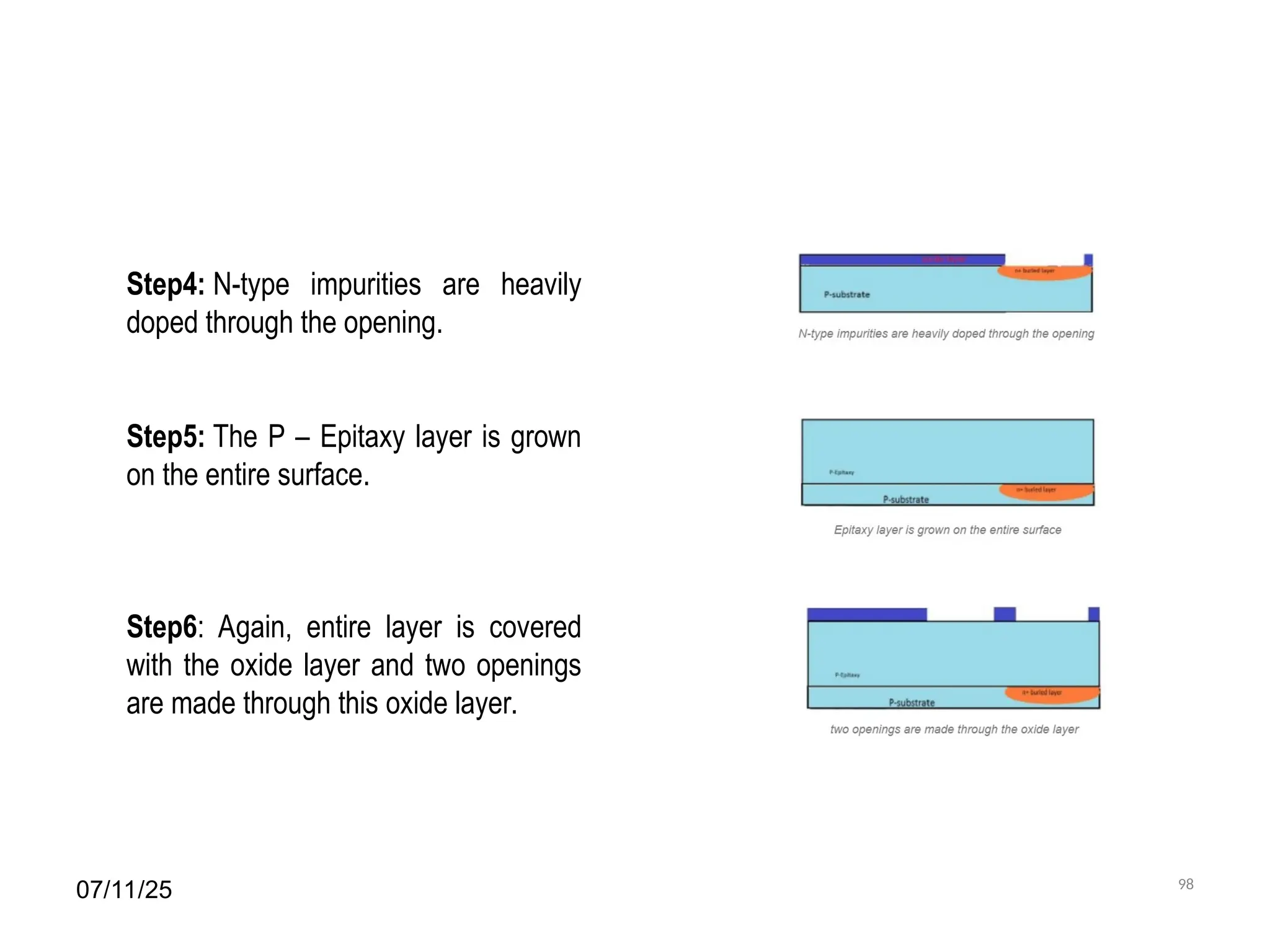
07/11/25 98
Step4: N-typeimpurities are heavily
doped through the opening.
Step5: The P – Epitaxy layer is grown
on the entire surface.
Step6: Again, entire layer is covered
with the oxide layer and two openings
are made through this oxide layer.
99.
07/11/25 99
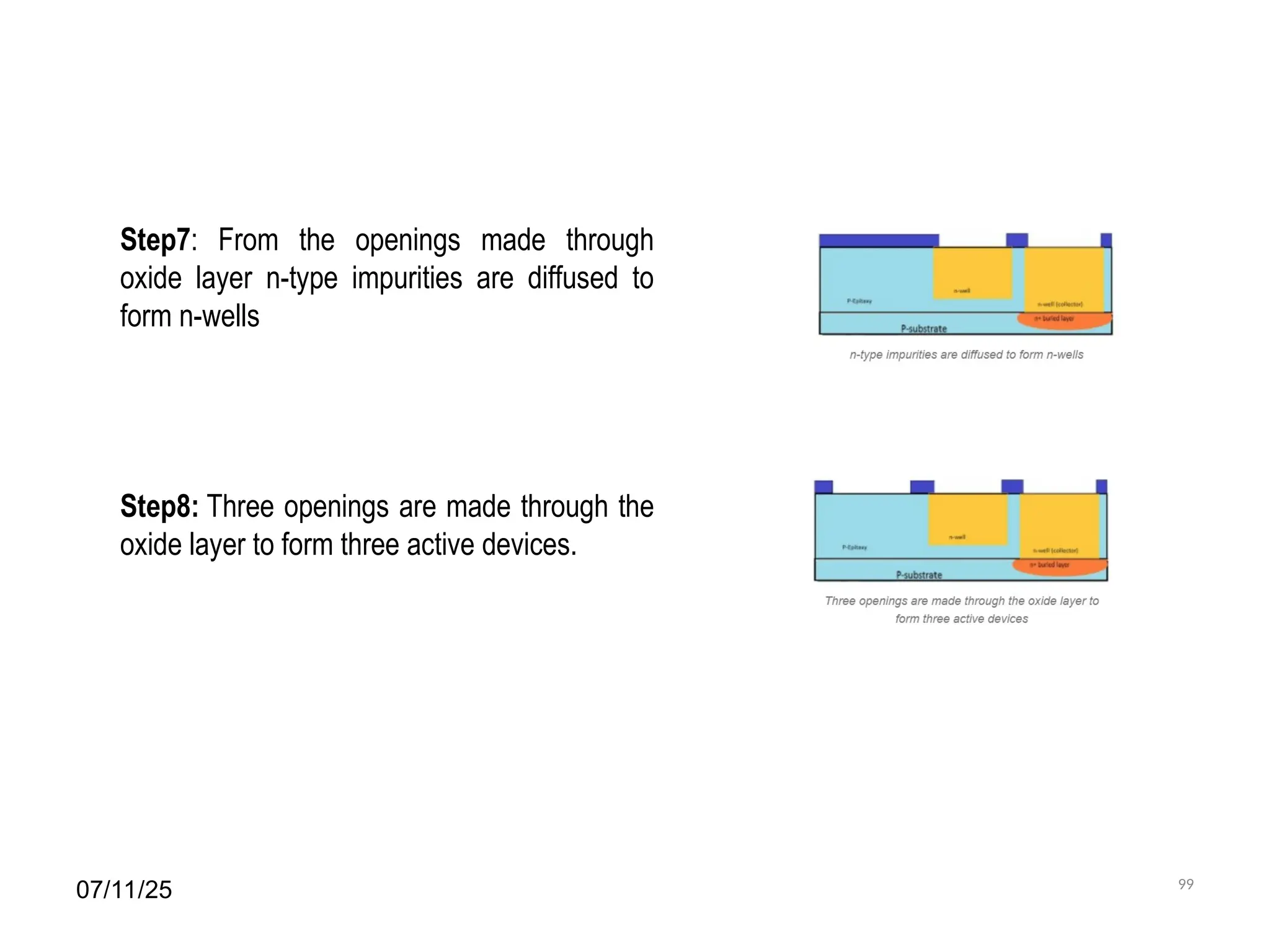
Step7: Fromthe openings made through
oxide layer n-type impurities are diffused to
form n-wells
Step8: Three openings are made through the
oxide layer to form three active devices.
100.
07/11/25 100
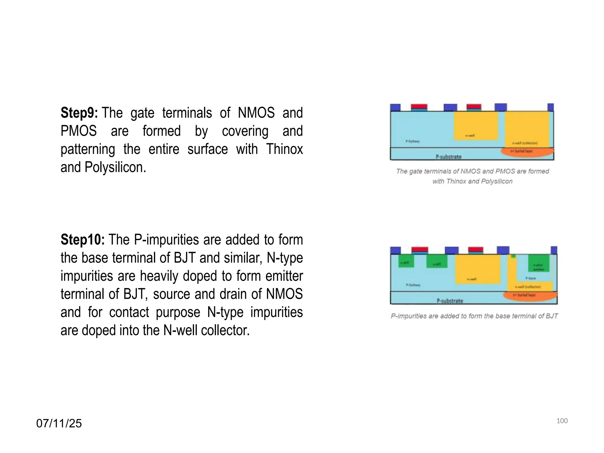
Step9: Thegate terminals of NMOS and
PMOS are formed by covering and
patterning the entire surface with Thinox
and Polysilicon.
Step10: The P-impurities are added to form
the base terminal of BJT and similar, N-type
impurities are heavily doped to form emitter
terminal of BJT, source and drain of NMOS
and for contact purpose N-type impurities
are doped into the N-well collector.
101.
07/11/25 101
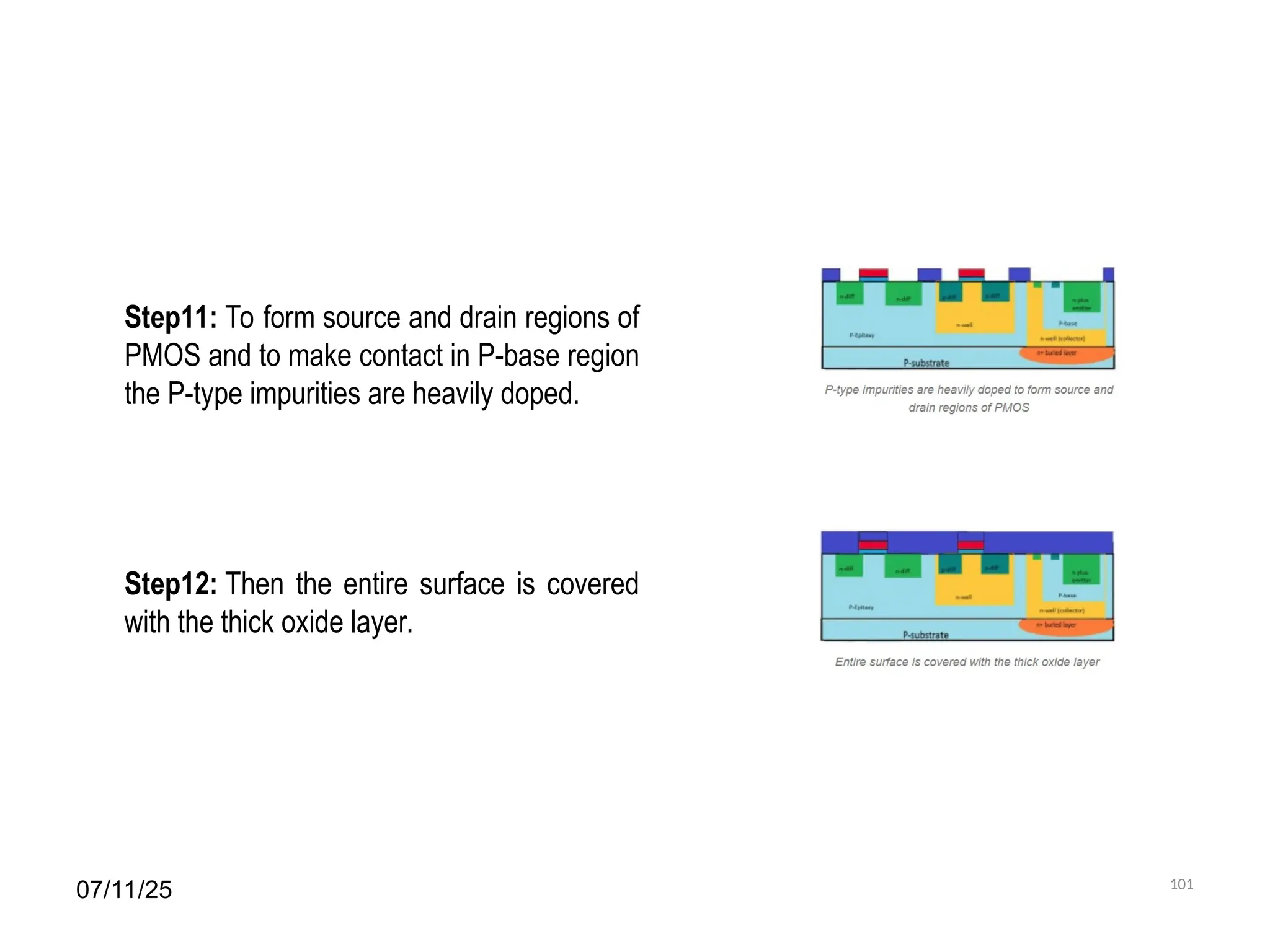
Step11: Toform source and drain regions of
PMOS and to make contact in P-base region
the P-type impurities are heavily doped.
Step12: Then the entire surface is covered
with the thick oxide layer.
102.
07/11/25 102
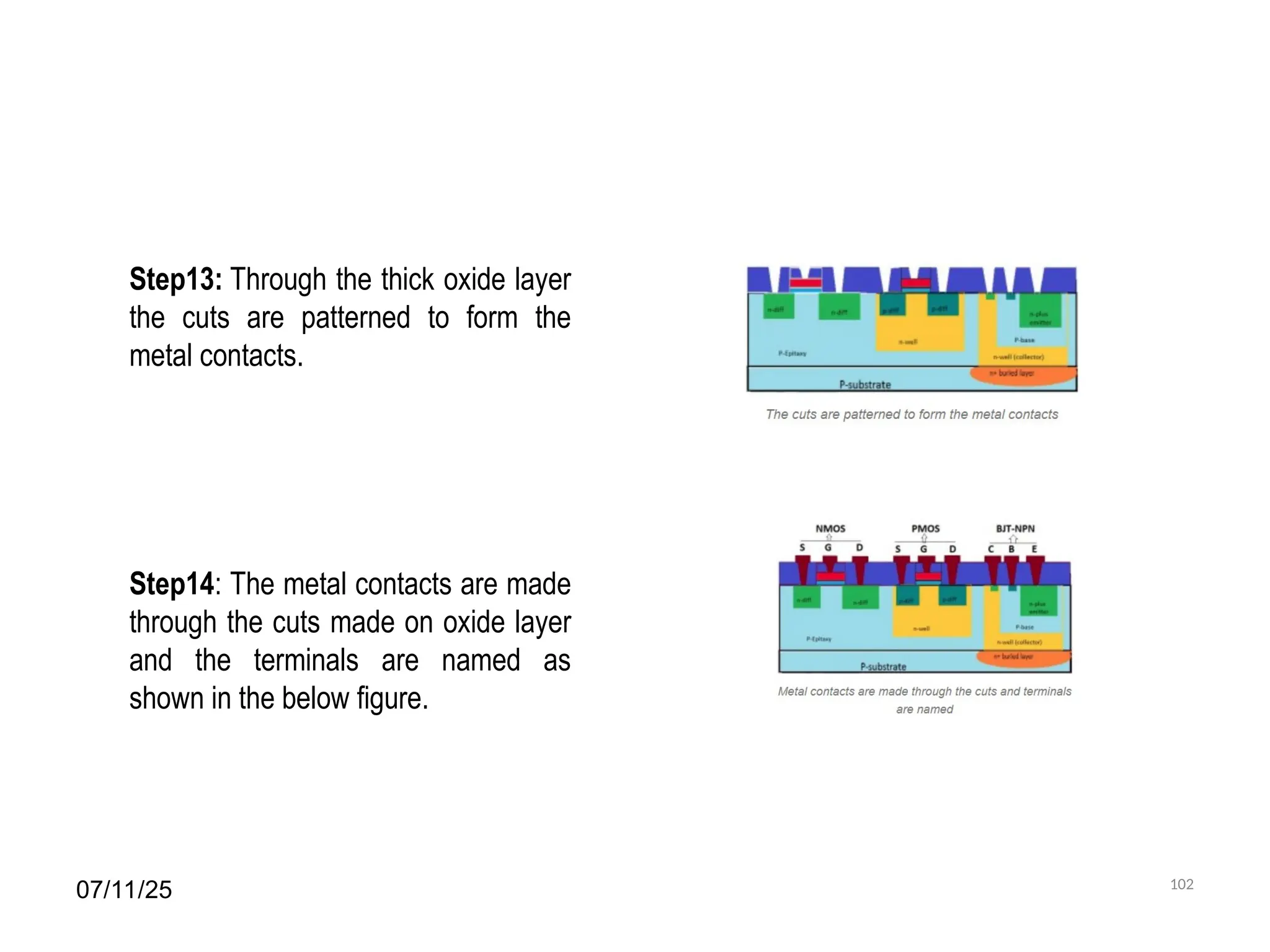
Step13: Throughthe thick oxide layer
the cuts are patterned to form the
metal contacts.
Step14: The metal contacts are made
through the cuts made on oxide layer
and the terminals are named as
shown in the below figure.
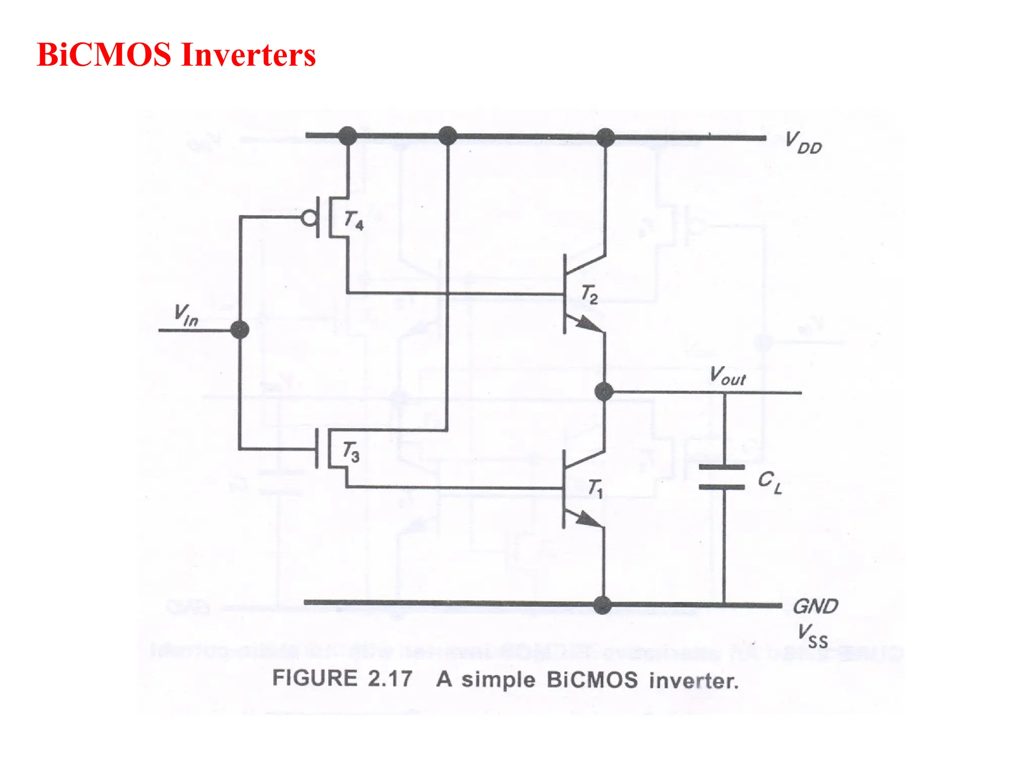
As in nMOSand CMOS logic circuitry, the basic logic
element is the inverter circuit.
When designing with BiCMOS in mind, the logical
approach is to use MOS switches to perform the logic function
and bipolar transistors to drive the output loads. The simplest
logic function is that of inversion, and a simple BiCMOS inverter
circuit is readily set out as shown in Figure 2.17.
It consists of two bipolar transistors T1 and T2 with one
nMOS transistor T3, and one pMOS transistor T4, both being
enhancement mode' devices. The action of the circuit is
straightforward and may be described as follows:
With Vin = 0 volts (GND) T3 is off so that T1 will be non-
conducting. But T4 is on and supplies current to the base of T2
which will conduct and act as a current source to charge the
load CL toward +5 volts (VDD). The output of the inverter will rise
to +5 volts less the base to emitter voltage V of T .
105.
With Vin =+5 volts (VDD) T4 is off so that T2 will be non-conducting. But
T3 will now be on and will supply current to the base of T) which will
conduct and act as a current sink to the load CL discharging it toward 0
volts (GND). The output of the inverter will fall to 0 volts plus the
saturation voltage VCEsatfrom the collector to the emitter of T1.
Tl and T2 will present low impedances when turned on into saturation
and the load CL will be charged or discharged rapidly.
The output logic levels will be good and will be close to the rail voltages
since VCEsat is quite small and VBE is approximately +0.7 volts.
The inverter has a high input impedance.
The inverter has a low output impedance.
The inverter has a high current drive capability but occupies a relatively
small area.
The inverter has high noise margins.
106.
However, owing tothe presence of a DC path from VDD to GND through T3
and T1, this is not a good arrangement to implement since there will be a
significant static current flow whenever Vin = logic 1. There is also a
problem in that there is no discharge path for current from the base of
either bipolar transistor when it is being turned off. This will slow down the
action of this circuit.
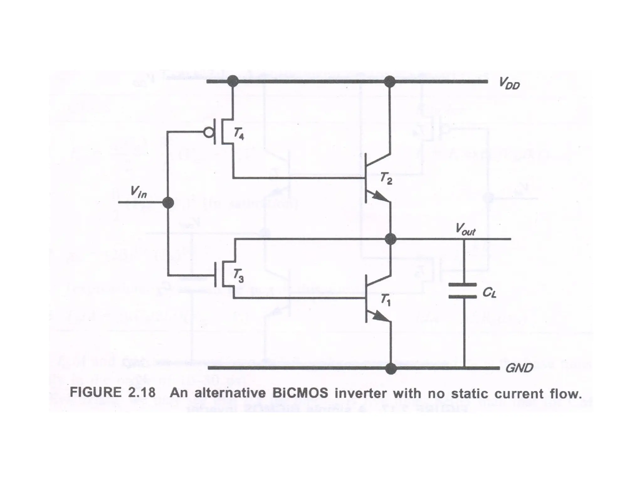
An improved version of this circuit is given in Figure 2.18, in which the DC
path through T3 and T1 is eliminated, but the output voltage swing is now
reduced, since the
output cannot fall below the base to emitter voltage VBE of T1.
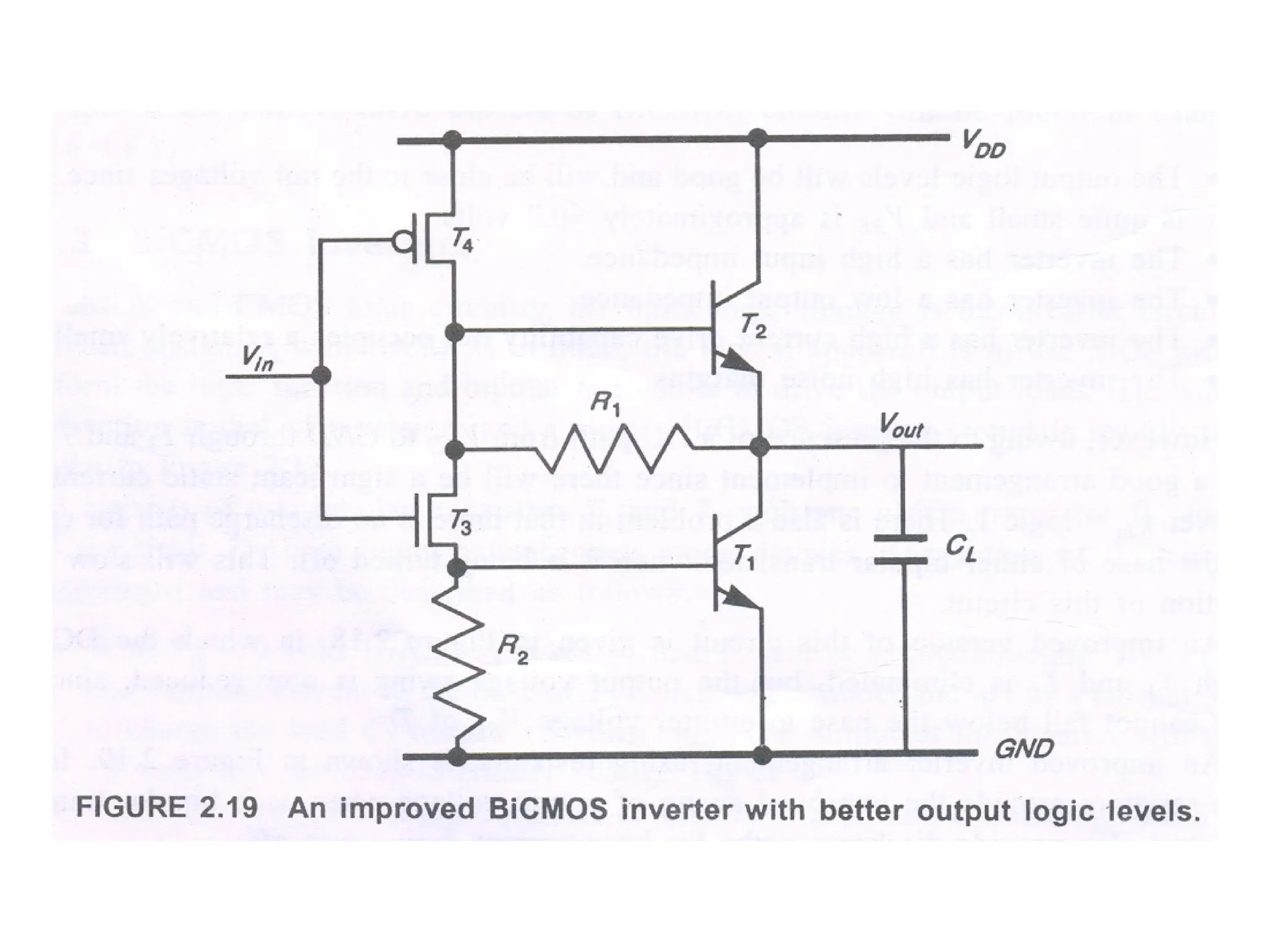
An improved inverter arrangement, using resistors, is shown in Figure
2.19. In this circuit resistors provide the improved swing of output voltage
when each bipolar transistor is off, and also provide discharge paths for
base current during turn-off.
The provision of on chip resistors of suitable value is not always
convenient and may be space-consuming, so that other arrangements-
such as in Figure 2.20-are used. In this circuit, the transistors Ts and T6
are arranged to turn on when T2 and T1 respectively are being turned off.
In general, BiCMOS inverters offer many advantages where high load
current sinking and sourcing is required. The arrangements lead on to the