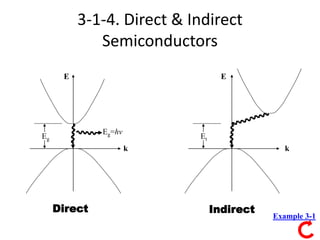
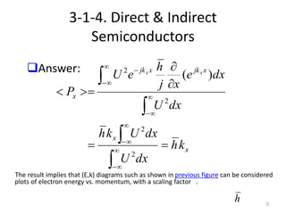
1) The document discusses direct and indirect semiconductors, explaining that direct semiconductors have a minimum energy (Eg) that occurs at the same crystal momentum (k) while indirect semiconductors have a minimum energy (Eg) that occurs at different k values.
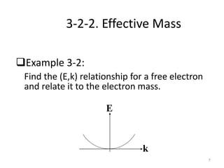
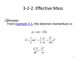
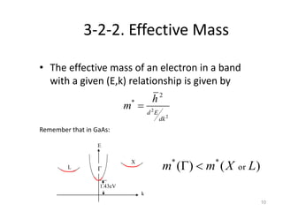
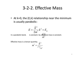
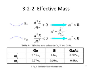
2) It also covers effective mass, which is used instead of free electron mass when applying equations of electrodynamics to charge carriers in solids. Effective mass depends on the curvature of the energy-momentum relationship.
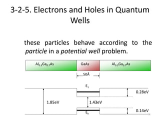
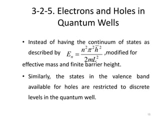
3) The document describes how electrons and holes behave as quantum particles when confined in a thin semiconductor layer between barriers of a different semiconductor, resulting in discrete energy levels instead of a continuum.