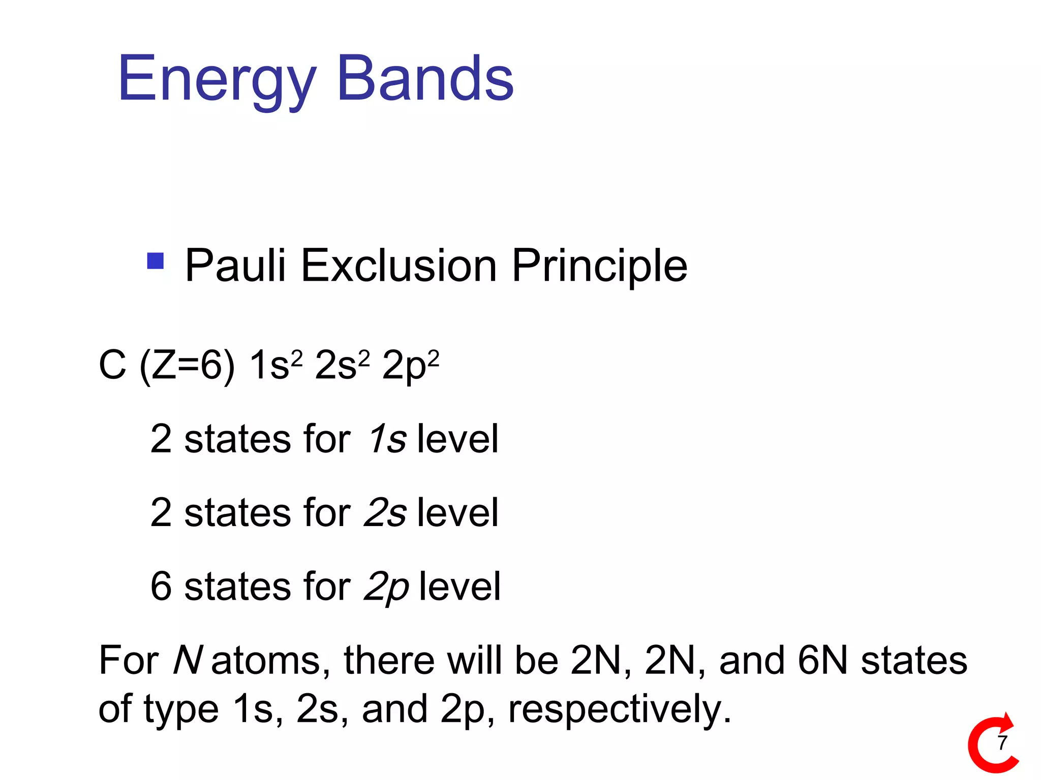
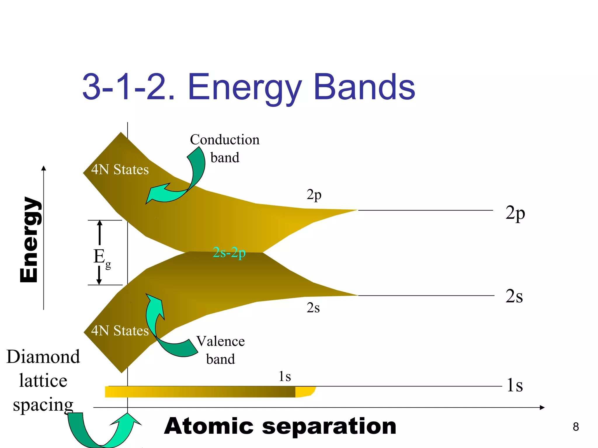
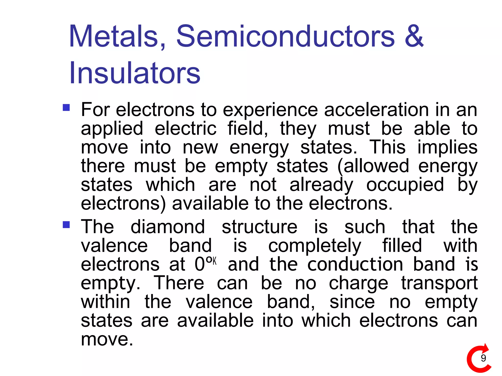
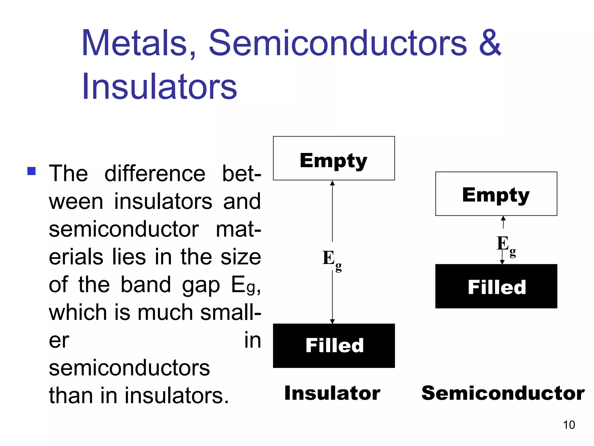
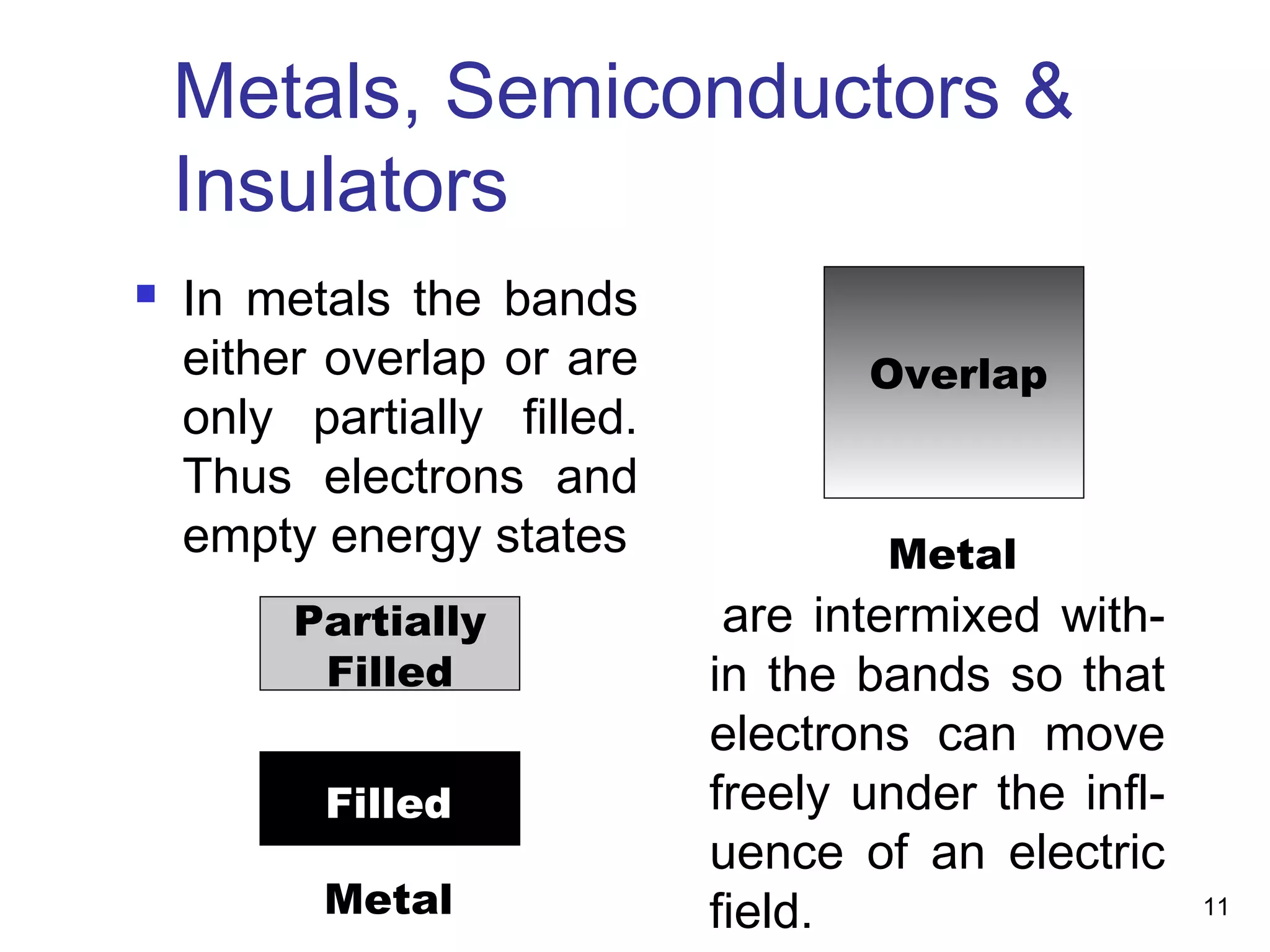
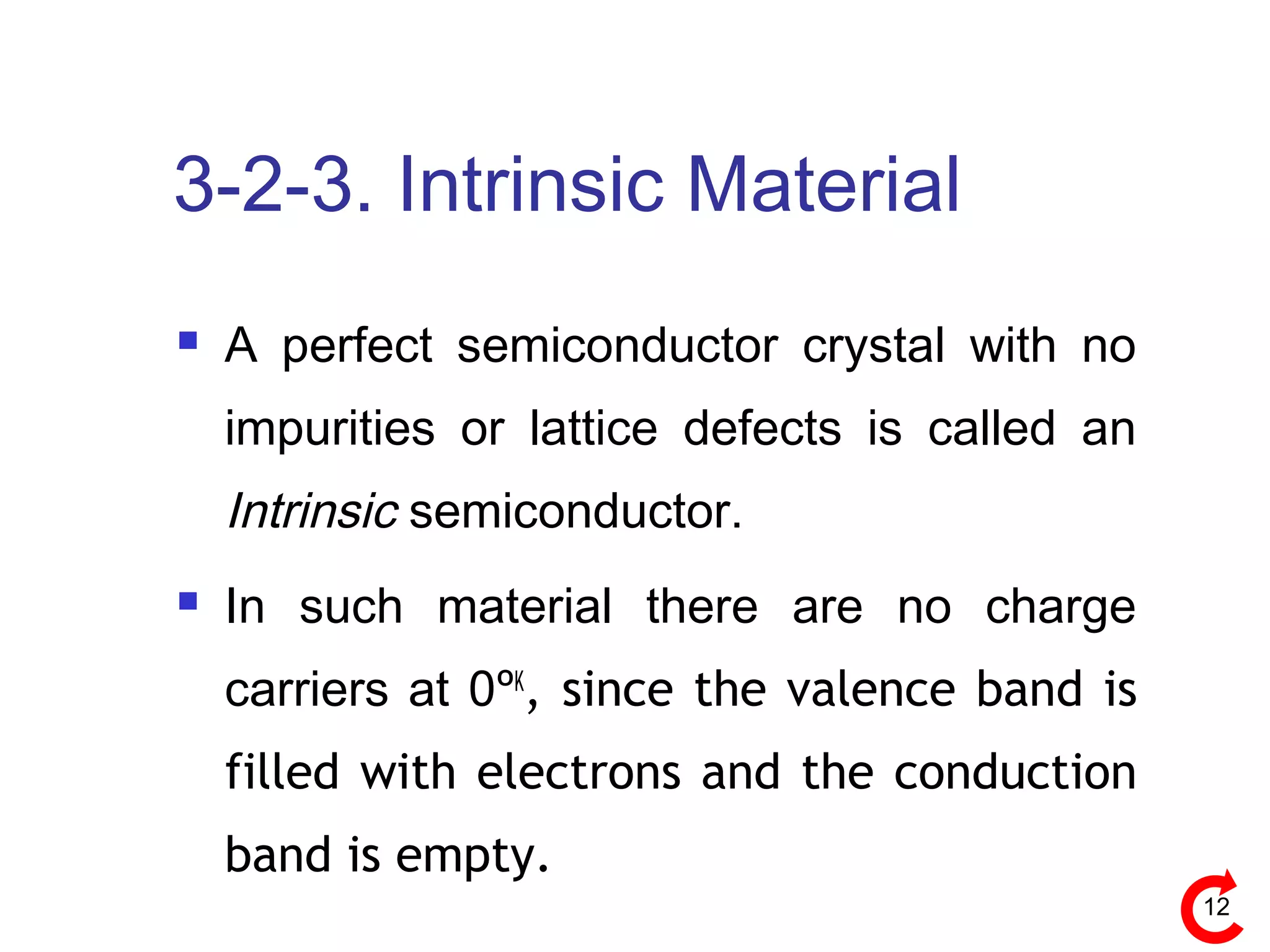
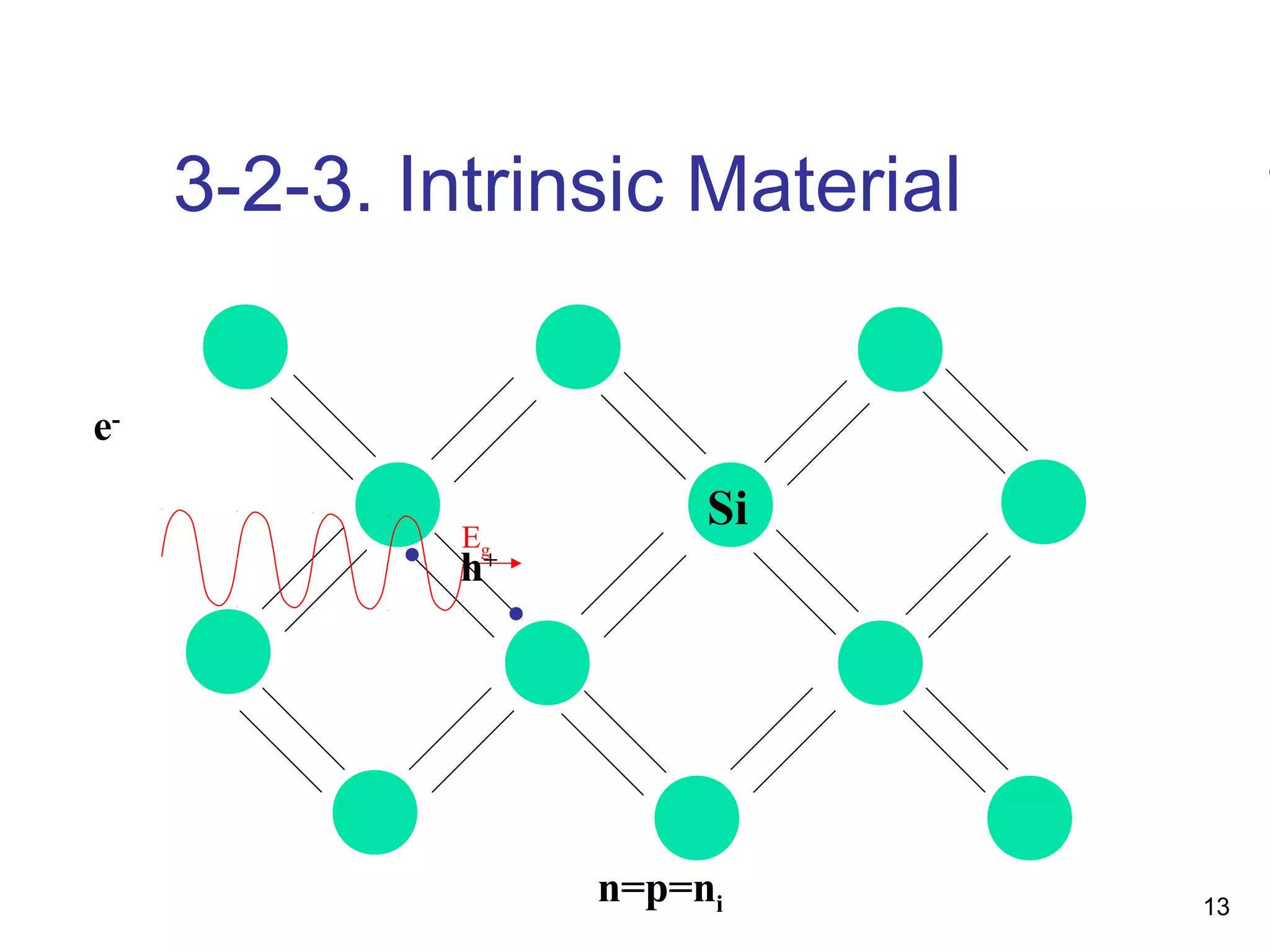
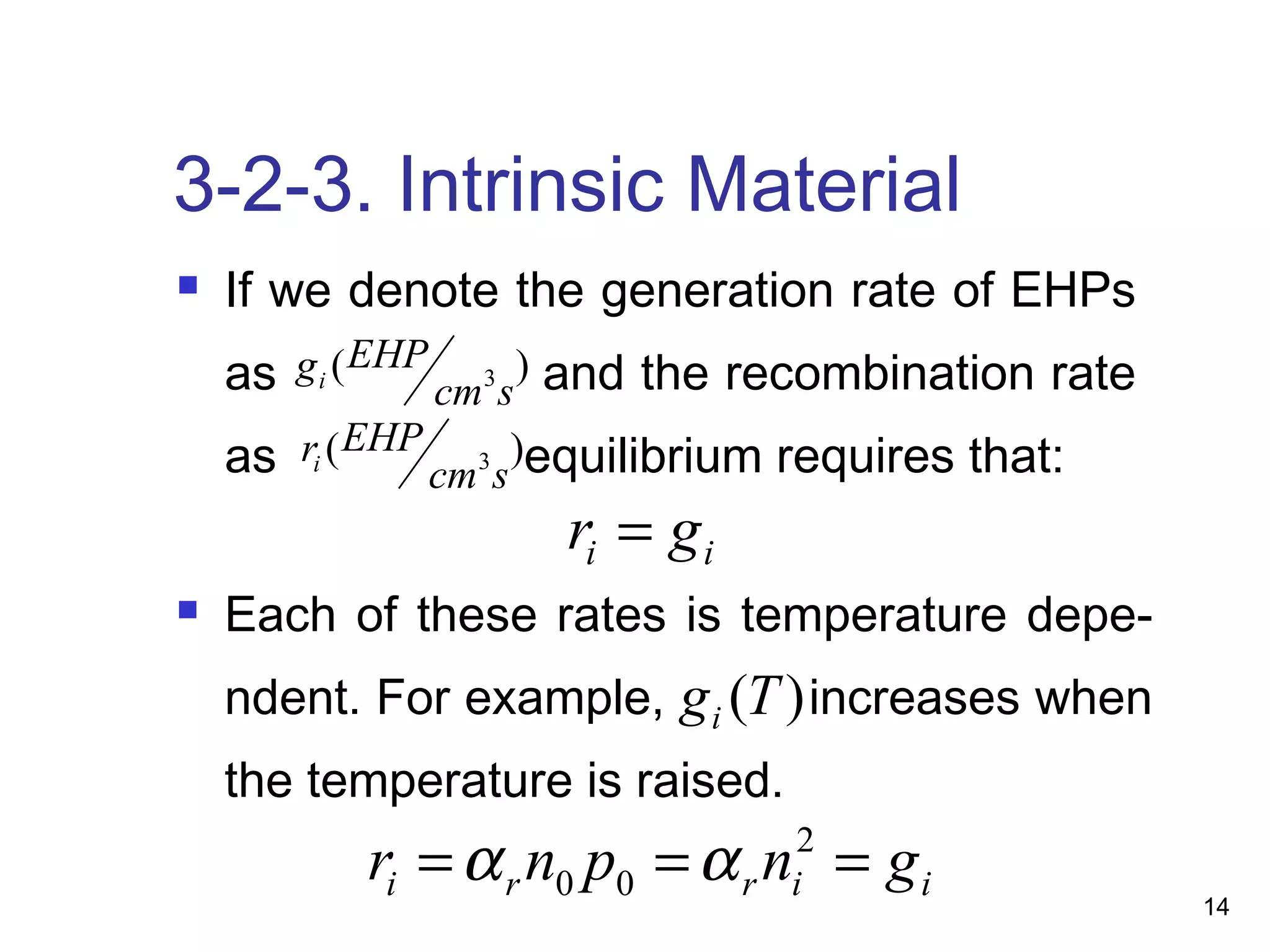
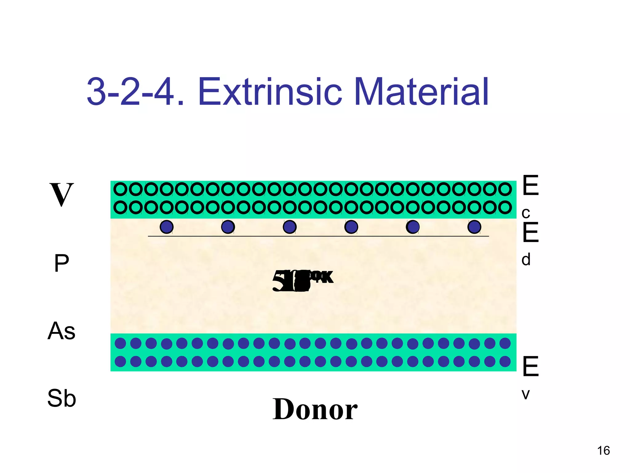
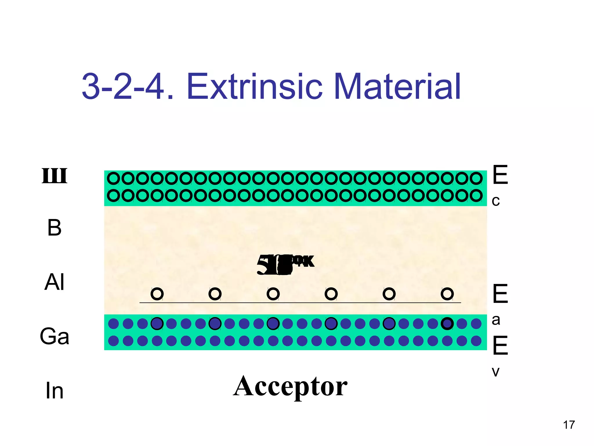
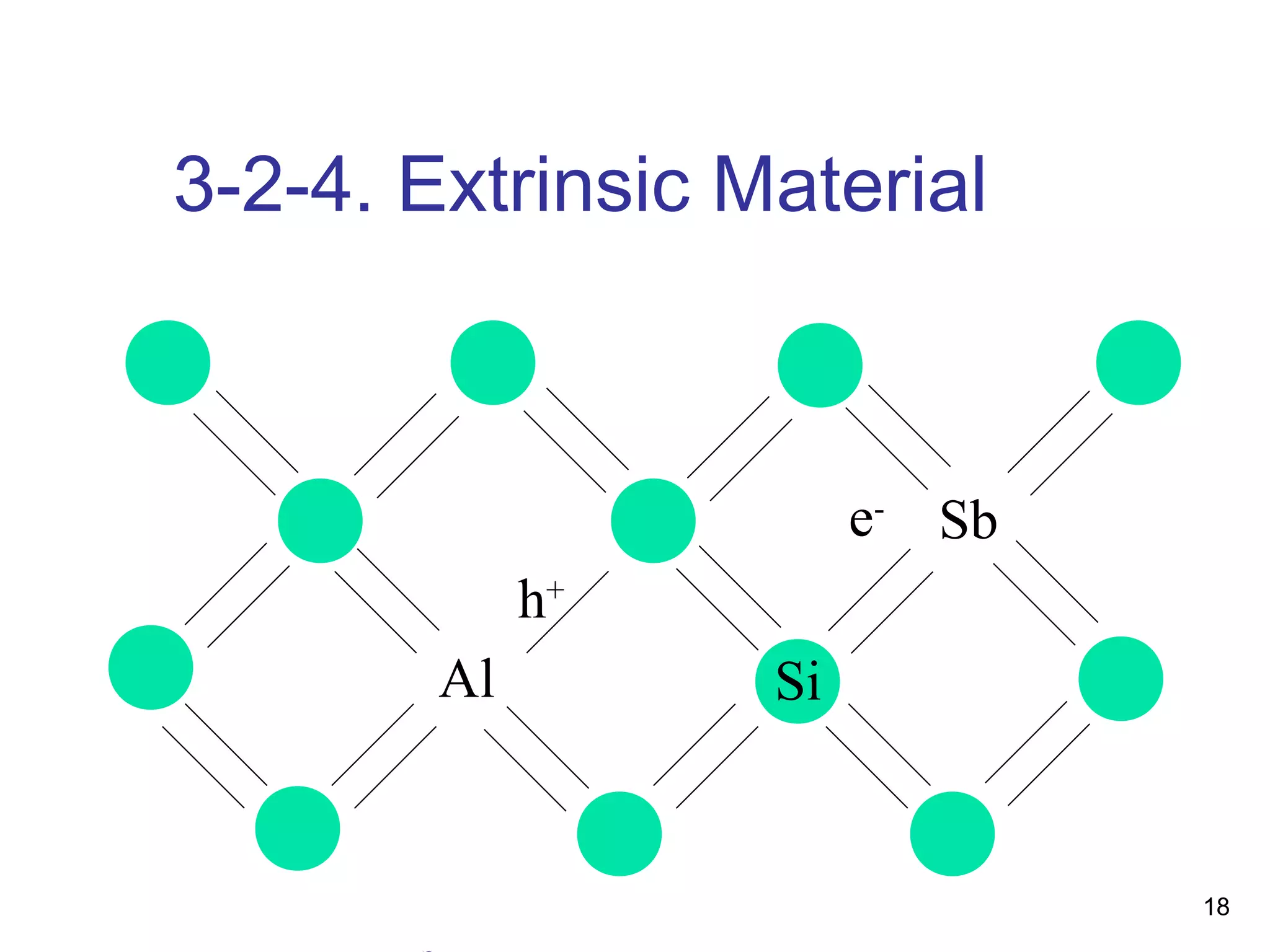
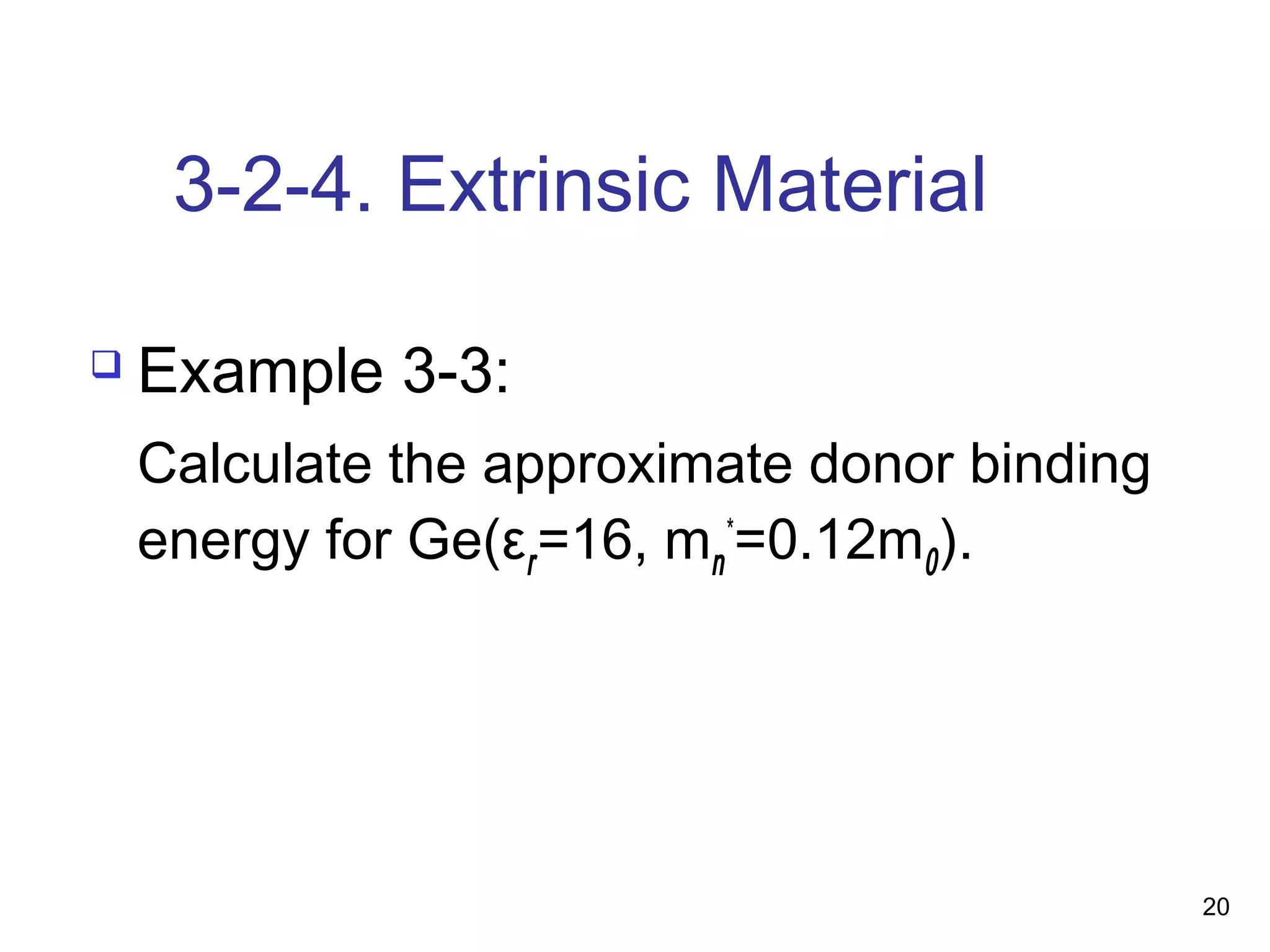
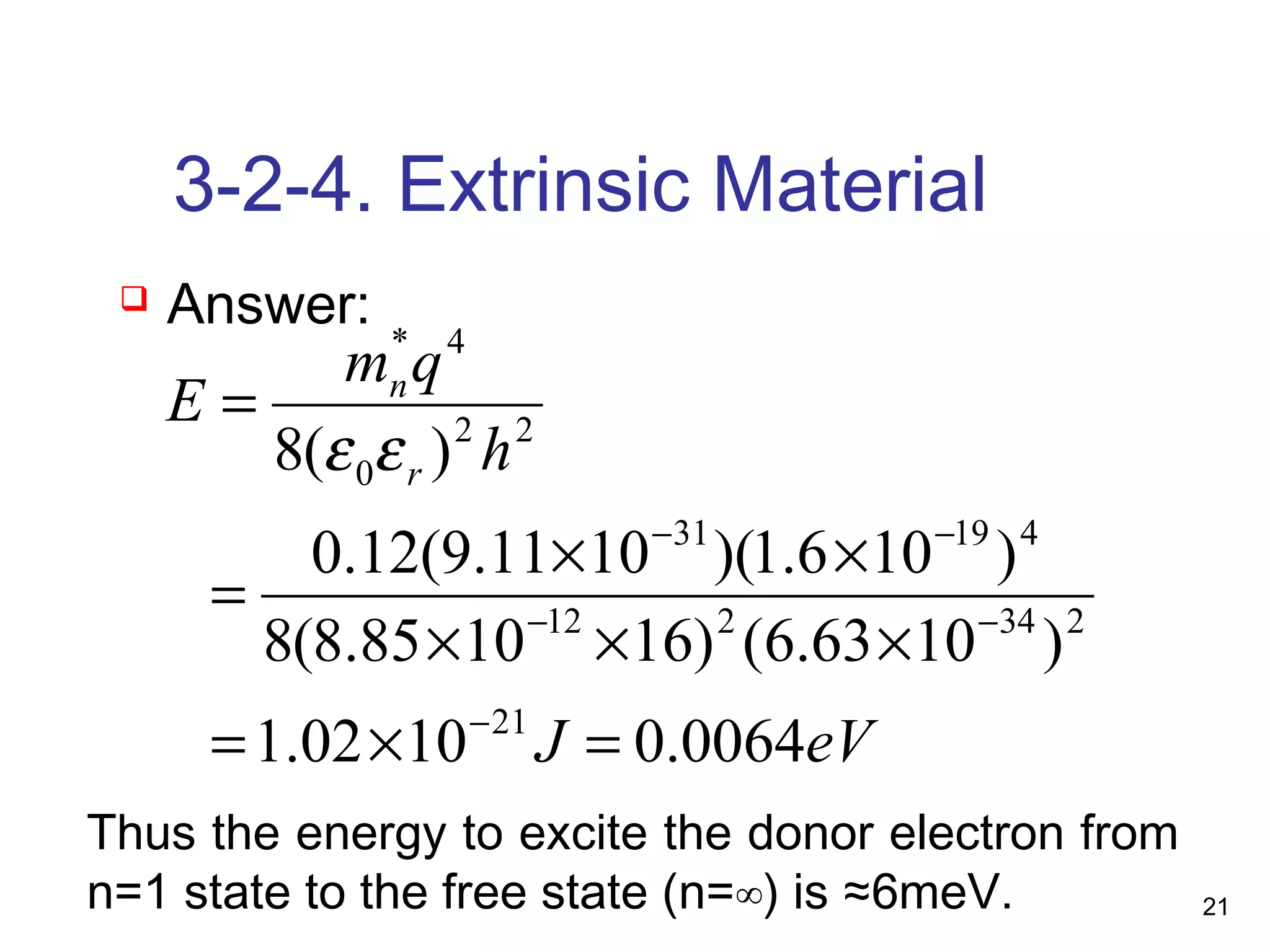
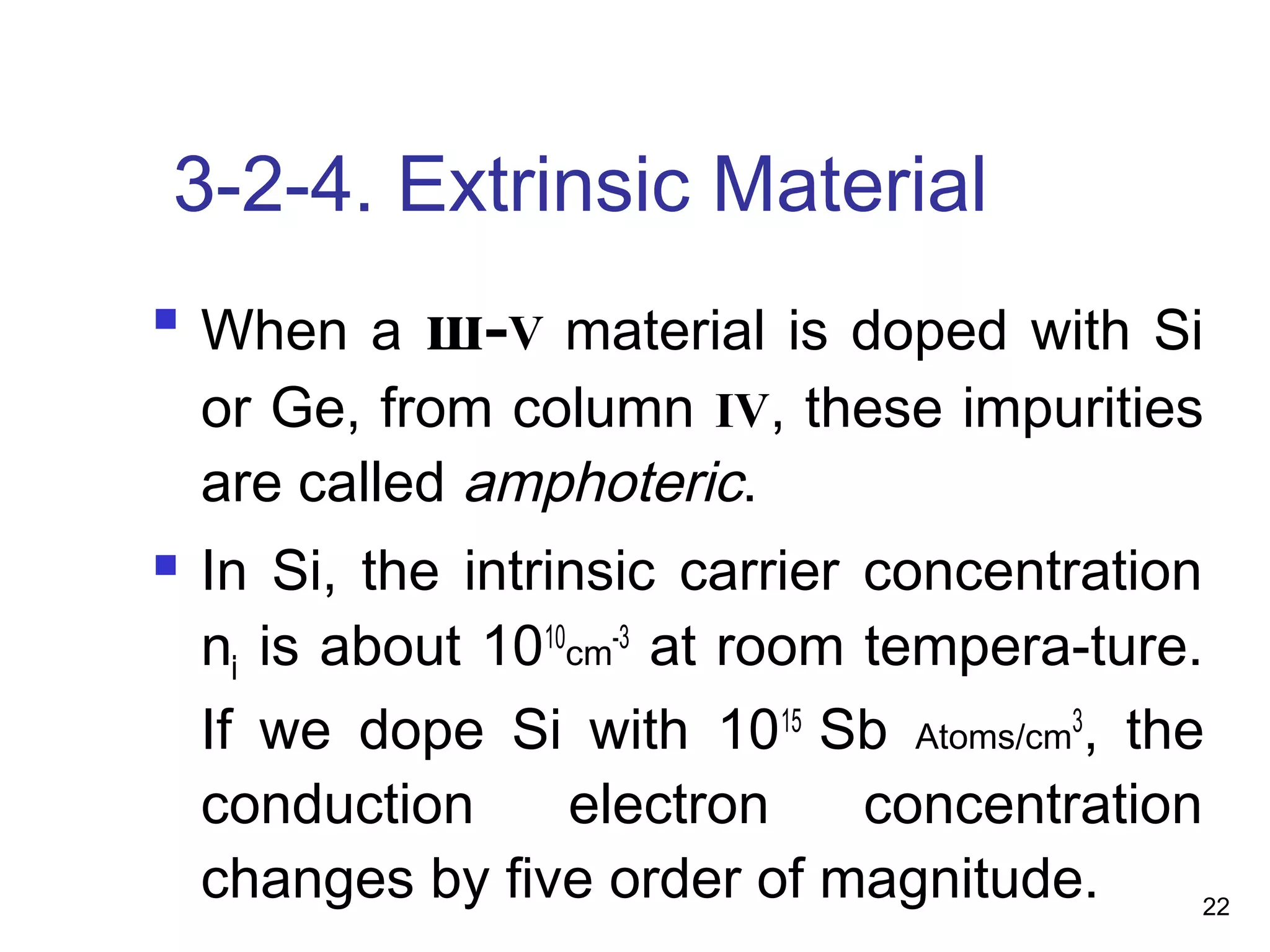
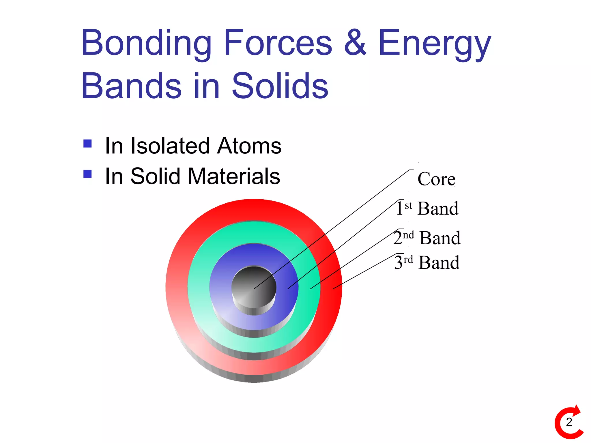
Energy bands and charge carriers in semiconductors describes how bonding forces in solids lead to the formation of energy bands. In intrinsic semiconductors, there is a small band gap between the valence and conduction bands, allowing a small number of electrons to be thermally excited across the gap. Extrinsic semiconductors are doped with impurities to introduce additional mobile charge carriers, making them either n-type or p-type and allowing electrical conductivity to be controlled. Doping introduces shallow impurity energy levels near the bands which donate or accept electrons.
![3
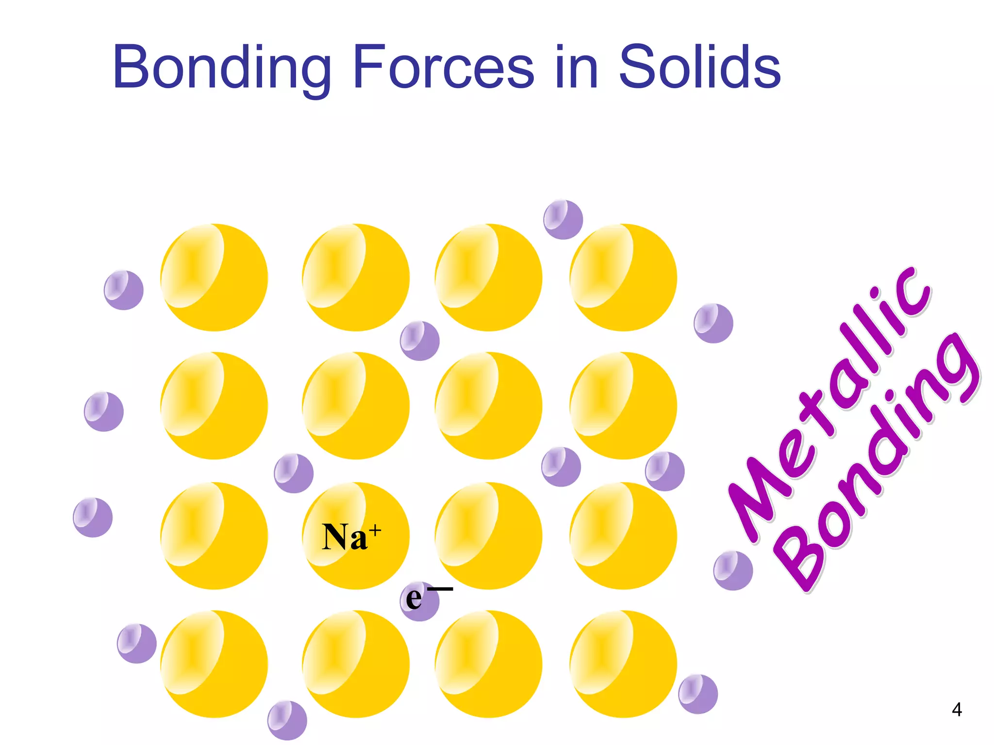
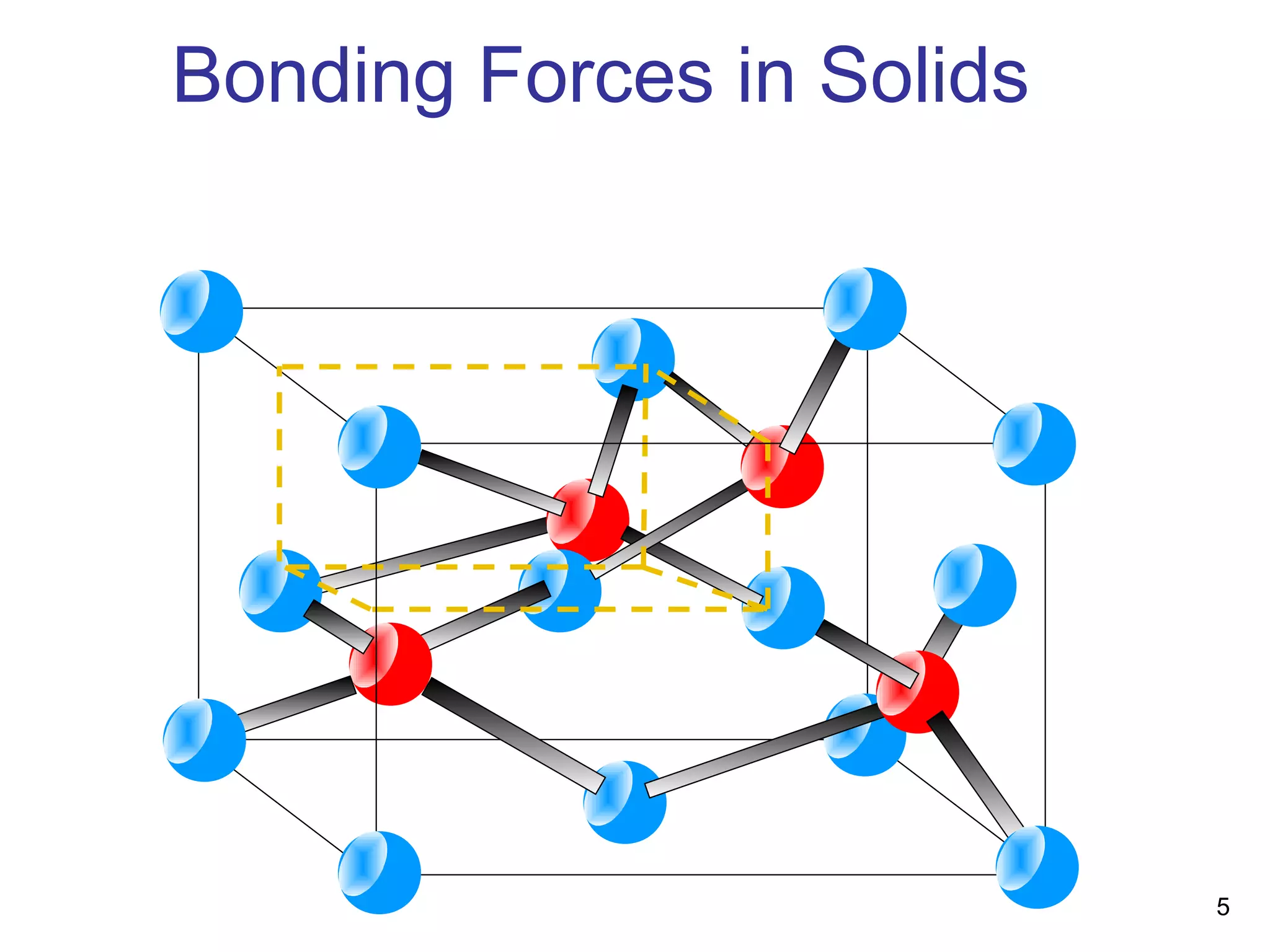
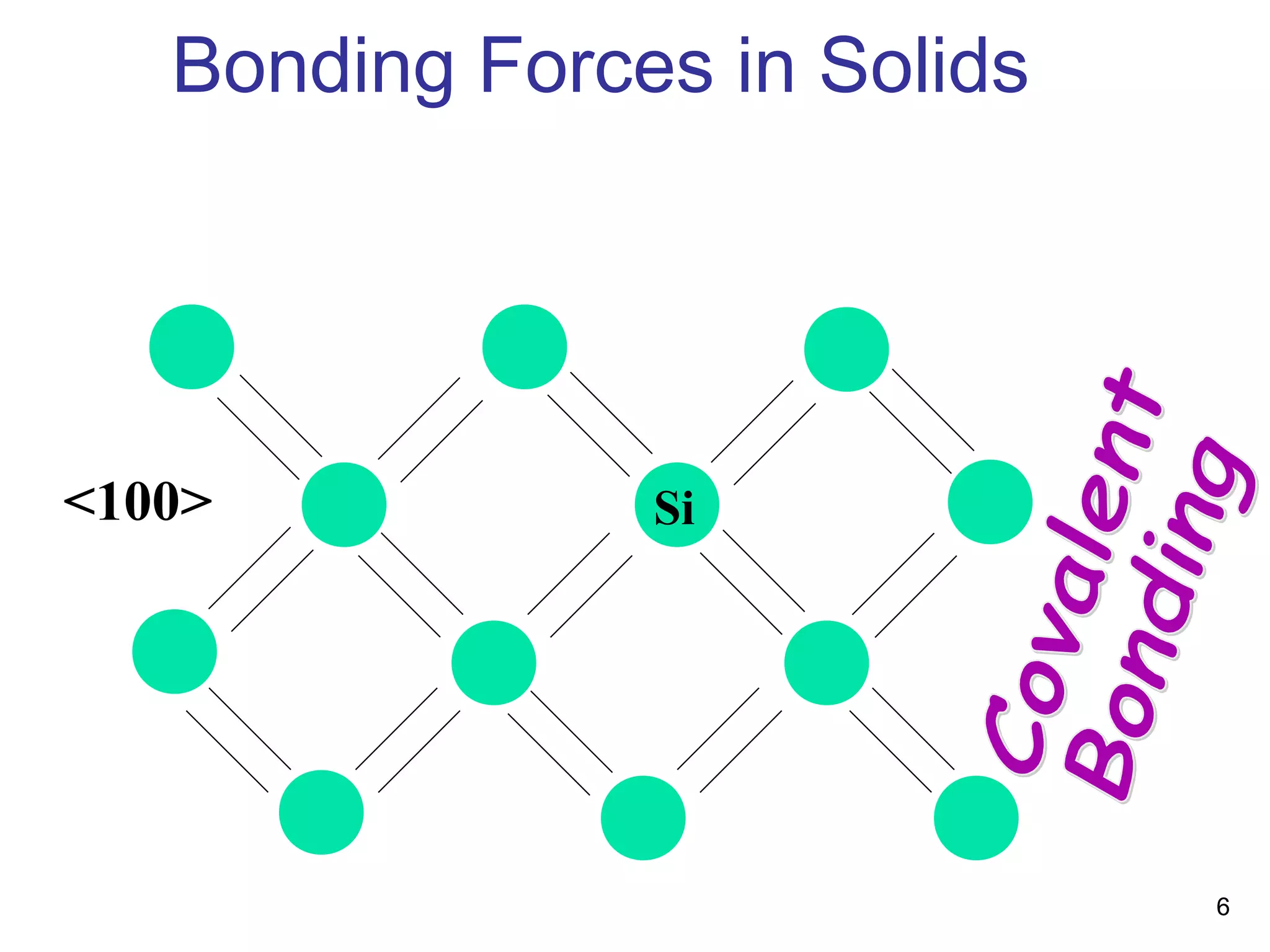
Bonding Forces in Solids
Na (Z=11) [Ne]3s1
Cl (Z=17) [Ne]3s1
3p5
Na+ Cl
_](https://image.slidesharecdn.com/lecture5energybandsandchargecarriers-140701034233-phpapp01/75/Lecture-5-energy-bands-and-charge-carriers-3-2048.jpg)