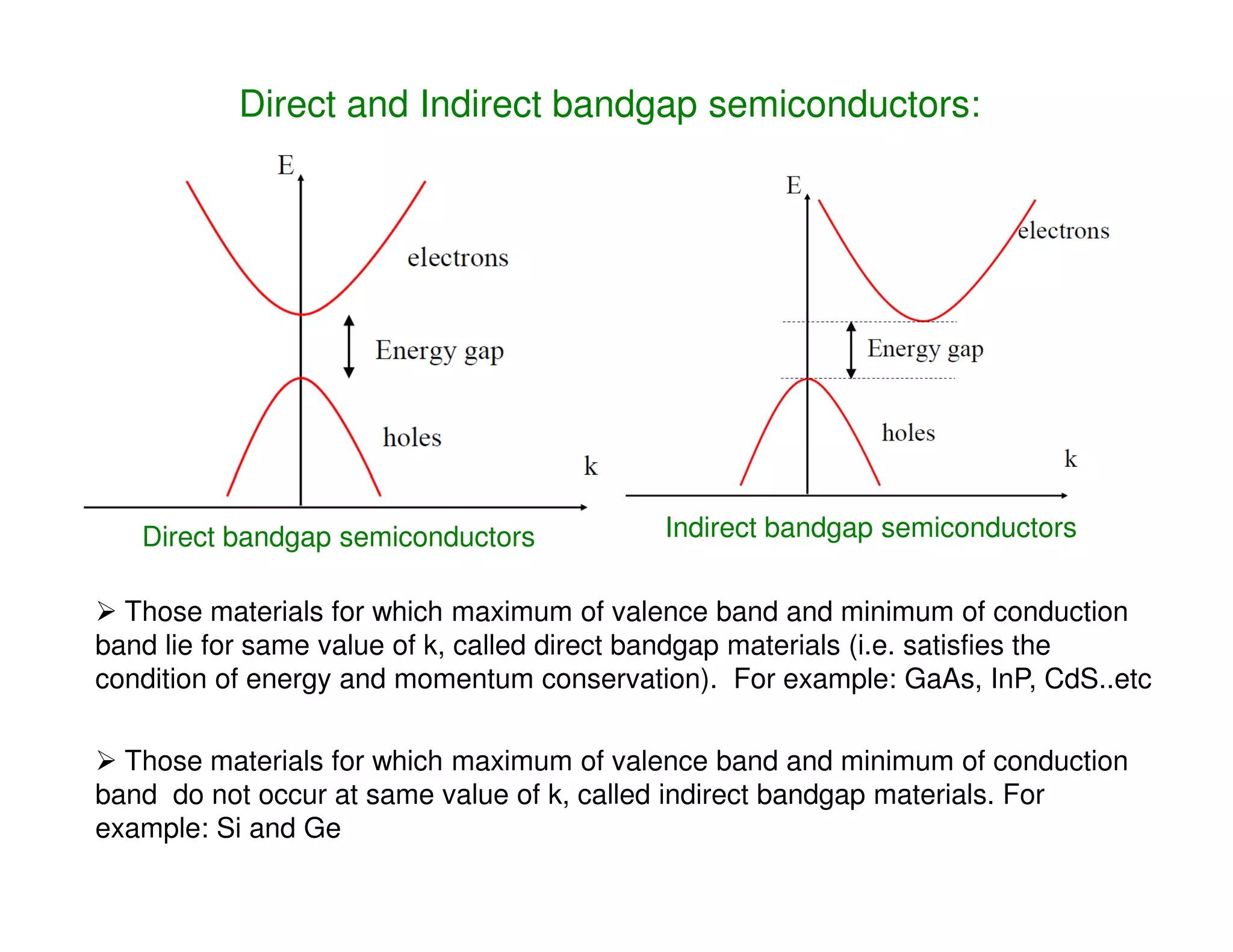
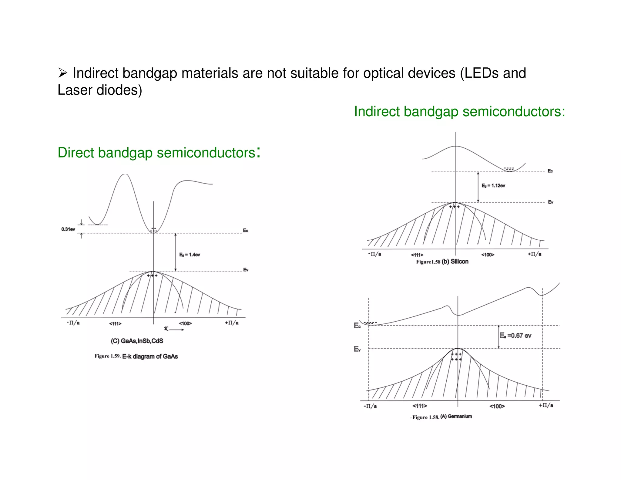
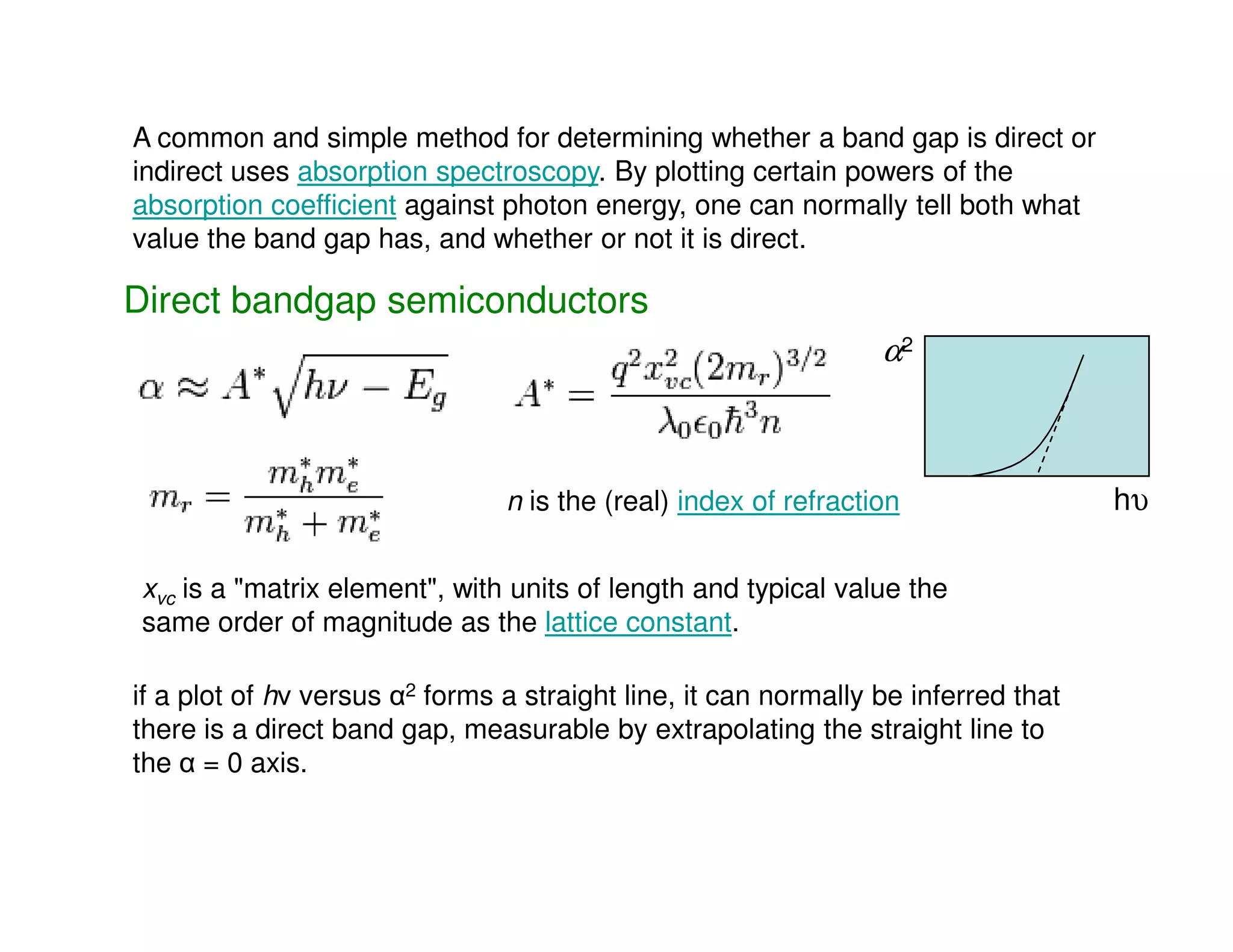
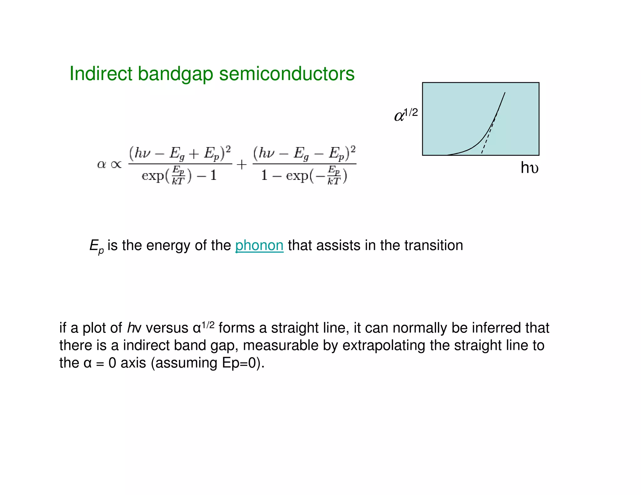
ANALOG & DIGITAL ELECTRONICS
Course No: PH-218
Tutorial -1
Course Instructor:
Dr. A.P. Vajpeyi
Department of Physics,
Indian Institute of Technology Guwahati, India
Direct and Indirect bandgap semiconductors:
Those materials for which maximum of valence band and minimum of conduction
band lie for same value of k, called direct bandgap materials (i.e. satisfies the
condition of energy and momentum conservation). For example: GaAs, InP, CdS..etc
Direct bandgap semiconductors Indirect bandgap semiconductors
Those materials for which maximum of valence band and minimum of conduction
band do not occur at same value of k, called indirect bandgap materials. For
example: Si and Ge
Indirect bandgap materials are not suitable for optical devices (LEDs and
Laser diodes)
Direct bandgap semiconductors:
Indirect bandgap semiconductors:
Direct bandgap semiconductors
A common and simple method for determining whether a band gap is direct or
indirect uses absorption spectroscopy. By plotting certain powers of the
absorption coefficient against photon energy, one can normally tell both what
value the band gap has, and whether or not it is direct.
α2
n is the (real) index of refraction
xvc is a "matrix element", with units of length and typical value the
same order of magnitude as the lattice constant.
if a plot of hν versus α2 forms a straight line, it can normally be inferred that
there is a direct band gap, measurable by extrapolating the straight line to
the α = 0 axis.
hυ
Indirect bandgap semiconductors
Ep is the energy of the phonon that assists in the transition
α1/2
hυ
Ep is the energy of the phonon that assists in the transition
if a plot of hν versus α1/2 forms a straight line, it can normally be inferred that
there is a indirect band gap, measurable by extrapolating the straight line to
the α = 0 axis (assuming Ep=0).
1D confinement: quantum wells; structures consisting of a thin well
materials sandwiched between two layers of a barrier materials.
2D confinement: quantum wires; structures consisting of a thin and
narrow well materials surrounded by barrier materials.
3D confinement: quantum dots; nano-size particles in a barrier
materials.
Why Nanomaterials ?
materials.
The quantum confinement => allowed electron and hole states are
quantized in the well region => energy required to generate e-h pair or
radiation emitted from the process of e-h pair recombination is modified
=> wavelength tuning of the radiation
(used in LED or laser applications)

Direct and in direct band gap-Modern Physics

  • 1.
    ANALOG & DIGITALELECTRONICS Course No: PH-218 Tutorial -1 Course Instructor: Dr. A.P. Vajpeyi Department of Physics, Indian Institute of Technology Guwahati, India
  • 2.
    Direct and Indirectbandgap semiconductors: Those materials for which maximum of valence band and minimum of conduction band lie for same value of k, called direct bandgap materials (i.e. satisfies the condition of energy and momentum conservation). For example: GaAs, InP, CdS..etc Direct bandgap semiconductors Indirect bandgap semiconductors Those materials for which maximum of valence band and minimum of conduction band do not occur at same value of k, called indirect bandgap materials. For example: Si and Ge
  • 3.
    Indirect bandgap materialsare not suitable for optical devices (LEDs and Laser diodes) Direct bandgap semiconductors: Indirect bandgap semiconductors:
  • 4.
    Direct bandgap semiconductors Acommon and simple method for determining whether a band gap is direct or indirect uses absorption spectroscopy. By plotting certain powers of the absorption coefficient against photon energy, one can normally tell both what value the band gap has, and whether or not it is direct. α2 n is the (real) index of refraction xvc is a "matrix element", with units of length and typical value the same order of magnitude as the lattice constant. if a plot of hν versus α2 forms a straight line, it can normally be inferred that there is a direct band gap, measurable by extrapolating the straight line to the α = 0 axis. hυ
  • 5.
    Indirect bandgap semiconductors Epis the energy of the phonon that assists in the transition α1/2 hυ Ep is the energy of the phonon that assists in the transition if a plot of hν versus α1/2 forms a straight line, it can normally be inferred that there is a indirect band gap, measurable by extrapolating the straight line to the α = 0 axis (assuming Ep=0).
  • 6.
    1D confinement: quantumwells; structures consisting of a thin well materials sandwiched between two layers of a barrier materials. 2D confinement: quantum wires; structures consisting of a thin and narrow well materials surrounded by barrier materials. 3D confinement: quantum dots; nano-size particles in a barrier materials. Why Nanomaterials ? materials. The quantum confinement => allowed electron and hole states are quantized in the well region => energy required to generate e-h pair or radiation emitted from the process of e-h pair recombination is modified => wavelength tuning of the radiation (used in LED or laser applications)