MAGNETRON SPUTTERING BASED THIN
FILMS FOR SOLAR CELLS
DEVENDRA BHALE
DBHALE@BARC.GOV.IN
SPUTTER DEPOSITION
• Magnetron sputtering is the most widely used method for vacuum
thin film deposition.
• Although the basic diode sputtering method (without magnetron or
magnetic enhanced) is still used in some application areas, magnetron
sputtering now serves over 90% of the market for sputter deposition.
• Magnetron sputtering can be used to coat virtually anything with a
wide range of materials - any solid metal or alloy and a variety of
compounds.
SPUTTERING SYSTEM
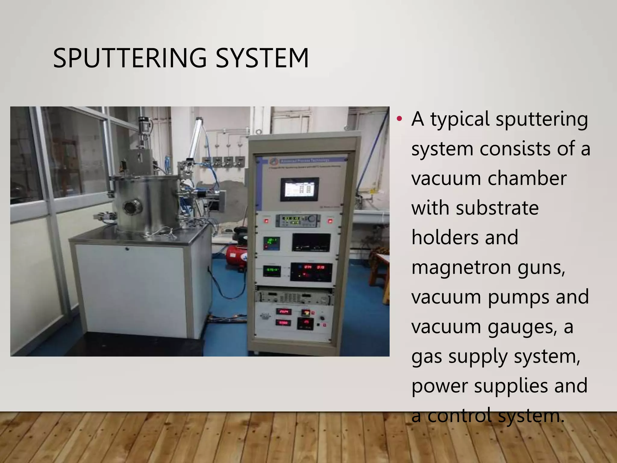
• A typical sputtering
system consists of a
vacuum chamber
with substrate
holders and
magnetron guns,
vacuum pumps and
vacuum gauges, a
gas supply system,
power supplies and
a control system.
THE PLASMA IN A MAGNETRON
• Plasma is called the fourth state of
matter after solid, liquid, and gas. It
is a state of matter in which an
ionized substance becomes highly
electrically conductive to the point
that long-range electric and magnetic
fields dominate its behavior.
• In many plasma coating applications
positive ions are generated by
collisions between neutral particles
and energetic electrons. The electrons
in a plasma are highly mobile,
especially compared to the larger ions
(typically argon for sputtering).
ref: www.gencoa.com
MICROSCOPIC VIEW OF SPUTTERING
• The impact of an atom or ion on a
surface produces sputtering from the
surface as a result of the momentum
transfer from the incoming particle.
Unlike many other vapor phase
techniques there is no melting of the
material.
• Phenomenon first described 150
years ago ...
Grove (1852) and plücker (1858) first
reported vaporization and film
formation of metal films by
sputtering.
• Other names for SPUTTERING were
SPLUTTERING and CATHODE
DESINTEGRATION.
THE MAGNETRON SPUTTER SOURCE
• A Magnetron is comprised is
used to confine plasma in front
of the target.
• Magnetic field
• An electrode (HV /RF)
• Target
PARAMETERS THAT CAN BE
CONTROLLED
• Kinetic energy of the incident ions & the sputtered
atoms
• Substrate temperature
• Deposition rate of thin film by changing either
• Input power
• Distance
• Gas scattering during transport of evaporant by
changing chamber pressure (1e-3mbar to 1e-2mbar)
MAGNETRON GUNS
WHAT IS THIN FILM
• A microscopically thin layer of material deposited on
to a metal, semiconductor, plastic or a ceramic base.
• Typical thickness of few nano meters to few microns.
• Can be conductive or nonconductive (dielectric)
• Applications include solar cell, Top metallic layer on a
chip, coating on a magnetic discs, hard coatings on
machine tools, antireflection layers on glasses etc.
THIN FILM SOLAR CELL
• Thin film based solar cells with relatively high
efficiency and low material usage is a promising
alternative for crystalline silicon technology.
• Easy to handle as it is flexible and can be formed on
complex shapes
• Cheaper than traditional technology, light weight easy
to move
• Thin film is better used during low light in shaded
areas
THE TYPICAL THIN FILM SOLAR
CELL
• Is made-up of multiple
layers
• Each layer has distinct
function and as to be
deposited with certain
key parameters
• Sputtering allows us to
deposit all these layers
THE ABSORBER LAYER
• The absorber layer is a semiconducting material often
considered the heart of all thin film solar cells.
• The absorber layers are like CIGS or CZTS
• The material is generally dielectric
• The thickness required is 1 to 10 microns
• The thin film should be uniform over large area
• The process should be stable and repeatable and
scalable
DEPOSITION OF CZTS ABSORBER
LAYER FROM A COMPOSITE TARGET
• The quaternary stoichiometric CZTS composite target is used
• The target is dielectric hence RF power supply is used
• The CZTS is deposited as tin film layer area of 25mm x 25mm
devices
• An efficiency of 5.2% has been achieved
• The process is reliable, industrially scalable
• Important process parameters pressure, stoichiometry of target,
substrate temperature, post processig
SPUTTERING INSULATORS AND
DIELECTRIC
• The thin film stoichiometry seen to be deviated from the ideal
stoichiometry
• The SEM images also reveal uniform thin film with grain size of
100-200nm size
OPTICAL TRANSMISSION SPECTRUM
• This study was done to get
effect of substrate
temperature o optical
properties
• The investigation shows a
strong effect of substrate
temperature during the
deposition on phase of the
thin film. The band gap has
reduced from 2.05 to 1.9 eV.
The band gap needs to be
~1.4eV for optimal solar cell
fabrication.
CO-SPUTTERING FROM MULTIPLE
TARGETS
• The CZTS precursor film
was co-sputtered using
three different targets;
copper (Cu), tin sulfide
(SnS / SnS2) and zinc
sulfide (ZnS).
• An efficiency of 6.6%
was obtiained
RESULTS
• The SEMM shows the
grain structure
• This route offers control
over stoichiometry and
phase of the CZTS
• The co-sputtering uses
DC power for copper
and RF power for
ZnS/SnS
MULTILAYER THIN FILMS AND
POST PROCESSING
• For CZTSSe solar cells
can produce flexible and
large-area modules with
homogeneous properties.
• A greater than 10%
efficiency for a cell area
larger than 2 cm2 of
certified flexible CZTSSe
solar cells
MULTILAYER SPUTTER DEPOSITION
• Metal precursors were deposited on the NaF layer using
99.99% pure Cu, Zn, and Sn sputtering targets with two
different stacking orders.
• The layers were deposited under sputtering powers of 150
W, 300 W, and 300W for the Cu, Zn, and Sn targets,
respectively, at a working pressure of 1 mTorr in an Ar
atmosphere
• The saples were post treatetd by sulpho-selenization using
pure Se and H2S gas
PREPARATION OF CZTS ABSORBER
LAYER BY REACTIVE SPUTTERING

09sputterdeposition.ppt

  • 1.
    MAGNETRON SPUTTERING BASEDTHIN FILMS FOR SOLAR CELLS DEVENDRA BHALE DBHALE@BARC.GOV.IN
  • 2.
    SPUTTER DEPOSITION • Magnetronsputtering is the most widely used method for vacuum thin film deposition. • Although the basic diode sputtering method (without magnetron or magnetic enhanced) is still used in some application areas, magnetron sputtering now serves over 90% of the market for sputter deposition. • Magnetron sputtering can be used to coat virtually anything with a wide range of materials - any solid metal or alloy and a variety of compounds.
  • 3.
    SPUTTERING SYSTEM • Atypical sputtering system consists of a vacuum chamber with substrate holders and magnetron guns, vacuum pumps and vacuum gauges, a gas supply system, power supplies and a control system.
  • 4.
    THE PLASMA INA MAGNETRON • Plasma is called the fourth state of matter after solid, liquid, and gas. It is a state of matter in which an ionized substance becomes highly electrically conductive to the point that long-range electric and magnetic fields dominate its behavior. • In many plasma coating applications positive ions are generated by collisions between neutral particles and energetic electrons. The electrons in a plasma are highly mobile, especially compared to the larger ions (typically argon for sputtering). ref: www.gencoa.com
  • 5.
    MICROSCOPIC VIEW OFSPUTTERING • The impact of an atom or ion on a surface produces sputtering from the surface as a result of the momentum transfer from the incoming particle. Unlike many other vapor phase techniques there is no melting of the material. • Phenomenon first described 150 years ago ... Grove (1852) and plücker (1858) first reported vaporization and film formation of metal films by sputtering. • Other names for SPUTTERING were SPLUTTERING and CATHODE DESINTEGRATION.
  • 6.
    THE MAGNETRON SPUTTERSOURCE • A Magnetron is comprised is used to confine plasma in front of the target. • Magnetic field • An electrode (HV /RF) • Target
  • 7.
    PARAMETERS THAT CANBE CONTROLLED • Kinetic energy of the incident ions & the sputtered atoms • Substrate temperature • Deposition rate of thin film by changing either • Input power • Distance • Gas scattering during transport of evaporant by changing chamber pressure (1e-3mbar to 1e-2mbar)
  • 8.
  • 9.
    WHAT IS THINFILM • A microscopically thin layer of material deposited on to a metal, semiconductor, plastic or a ceramic base. • Typical thickness of few nano meters to few microns. • Can be conductive or nonconductive (dielectric) • Applications include solar cell, Top metallic layer on a chip, coating on a magnetic discs, hard coatings on machine tools, antireflection layers on glasses etc.
  • 10.
    THIN FILM SOLARCELL • Thin film based solar cells with relatively high efficiency and low material usage is a promising alternative for crystalline silicon technology. • Easy to handle as it is flexible and can be formed on complex shapes • Cheaper than traditional technology, light weight easy to move • Thin film is better used during low light in shaded areas
  • 11.
    THE TYPICAL THINFILM SOLAR CELL • Is made-up of multiple layers • Each layer has distinct function and as to be deposited with certain key parameters • Sputtering allows us to deposit all these layers
  • 12.
    THE ABSORBER LAYER •The absorber layer is a semiconducting material often considered the heart of all thin film solar cells. • The absorber layers are like CIGS or CZTS • The material is generally dielectric • The thickness required is 1 to 10 microns • The thin film should be uniform over large area • The process should be stable and repeatable and scalable
  • 13.
    DEPOSITION OF CZTSABSORBER LAYER FROM A COMPOSITE TARGET • The quaternary stoichiometric CZTS composite target is used • The target is dielectric hence RF power supply is used • The CZTS is deposited as tin film layer area of 25mm x 25mm devices • An efficiency of 5.2% has been achieved • The process is reliable, industrially scalable • Important process parameters pressure, stoichiometry of target, substrate temperature, post processig
  • 14.
    SPUTTERING INSULATORS AND DIELECTRIC •The thin film stoichiometry seen to be deviated from the ideal stoichiometry • The SEM images also reveal uniform thin film with grain size of 100-200nm size
  • 15.
    OPTICAL TRANSMISSION SPECTRUM •This study was done to get effect of substrate temperature o optical properties • The investigation shows a strong effect of substrate temperature during the deposition on phase of the thin film. The band gap has reduced from 2.05 to 1.9 eV. The band gap needs to be ~1.4eV for optimal solar cell fabrication.
  • 16.
    CO-SPUTTERING FROM MULTIPLE TARGETS •The CZTS precursor film was co-sputtered using three different targets; copper (Cu), tin sulfide (SnS / SnS2) and zinc sulfide (ZnS). • An efficiency of 6.6% was obtiained
  • 17.
    RESULTS • The SEMMshows the grain structure • This route offers control over stoichiometry and phase of the CZTS • The co-sputtering uses DC power for copper and RF power for ZnS/SnS
  • 18.
    MULTILAYER THIN FILMSAND POST PROCESSING • For CZTSSe solar cells can produce flexible and large-area modules with homogeneous properties. • A greater than 10% efficiency for a cell area larger than 2 cm2 of certified flexible CZTSSe solar cells
  • 19.
    MULTILAYER SPUTTER DEPOSITION •Metal precursors were deposited on the NaF layer using 99.99% pure Cu, Zn, and Sn sputtering targets with two different stacking orders. • The layers were deposited under sputtering powers of 150 W, 300 W, and 300W for the Cu, Zn, and Sn targets, respectively, at a working pressure of 1 mTorr in an Ar atmosphere • The saples were post treatetd by sulpho-selenization using pure Se and H2S gas
  • 20.
    PREPARATION OF CZTSABSORBER LAYER BY REACTIVE SPUTTERING