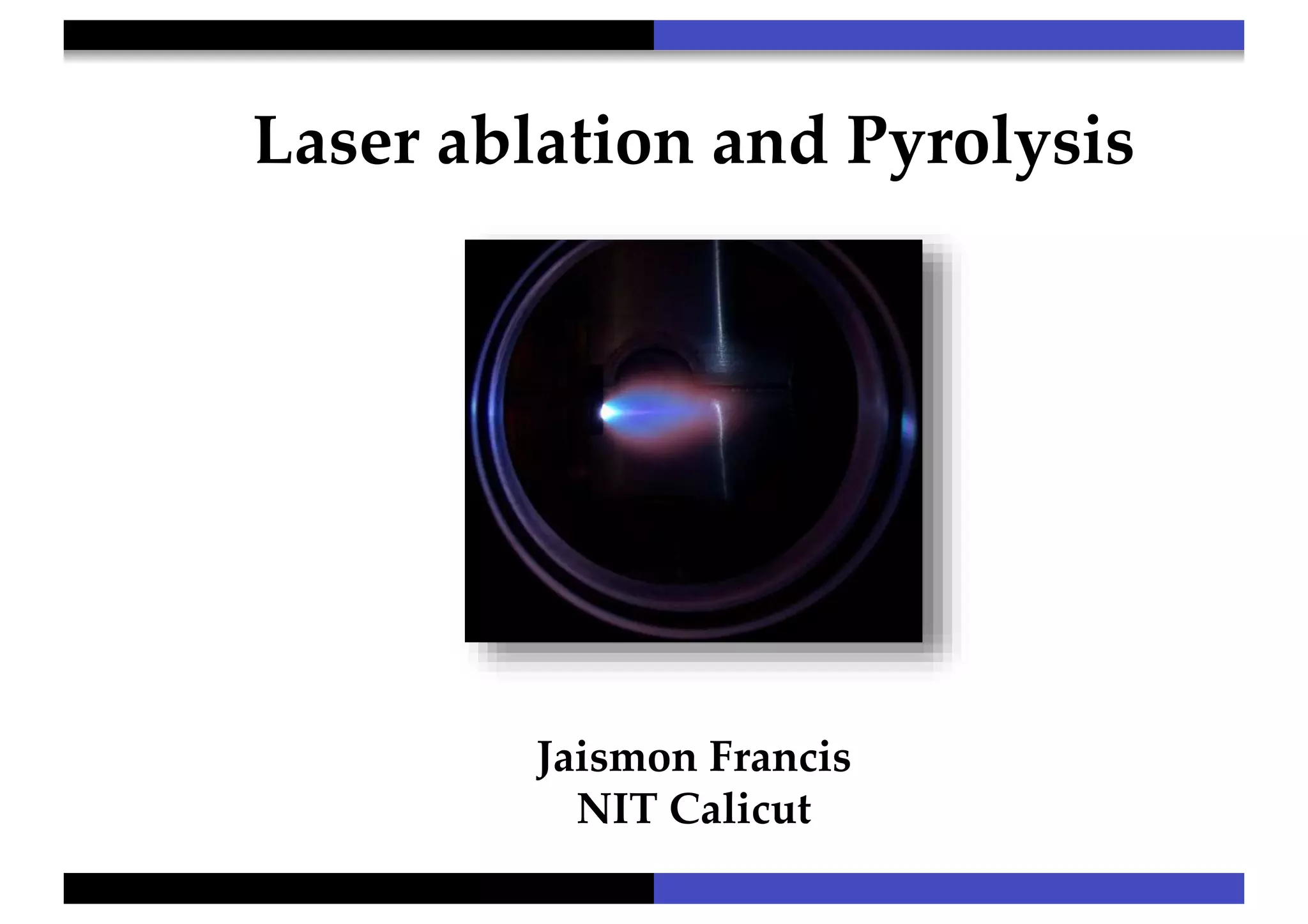
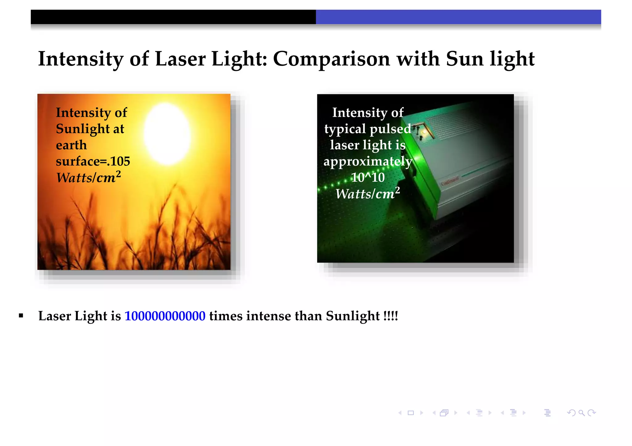
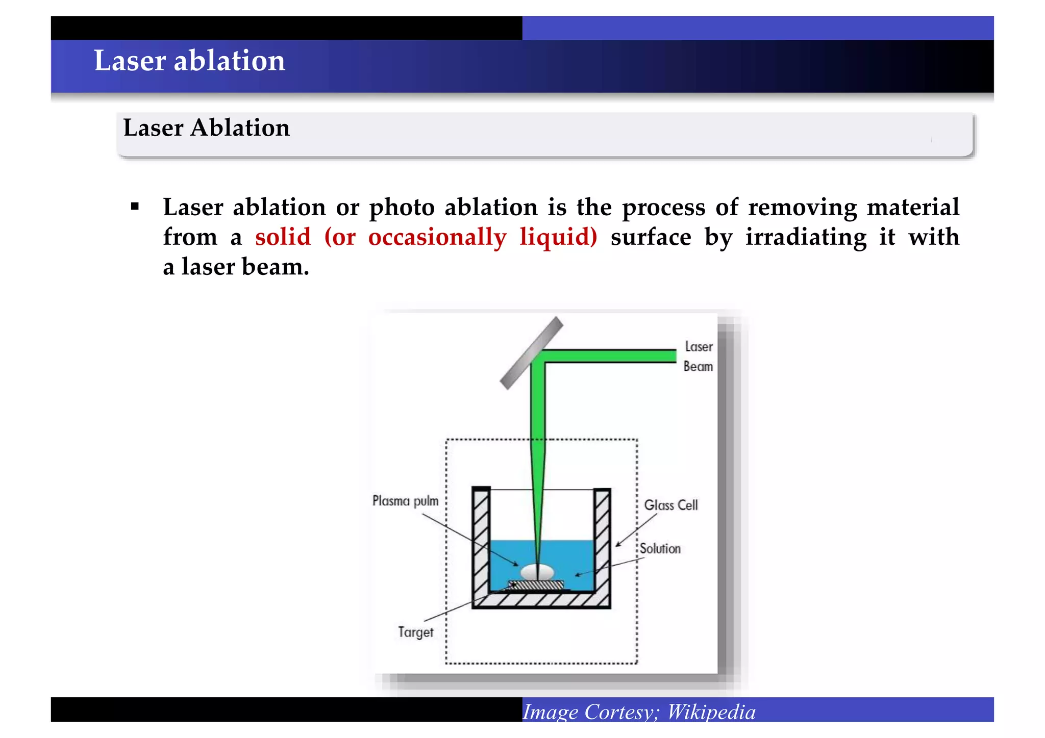
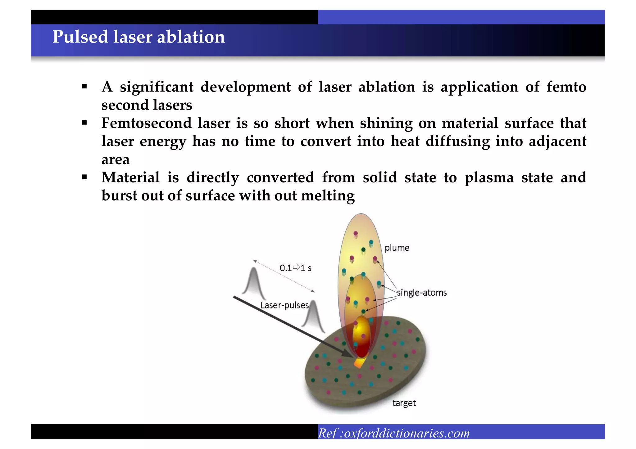
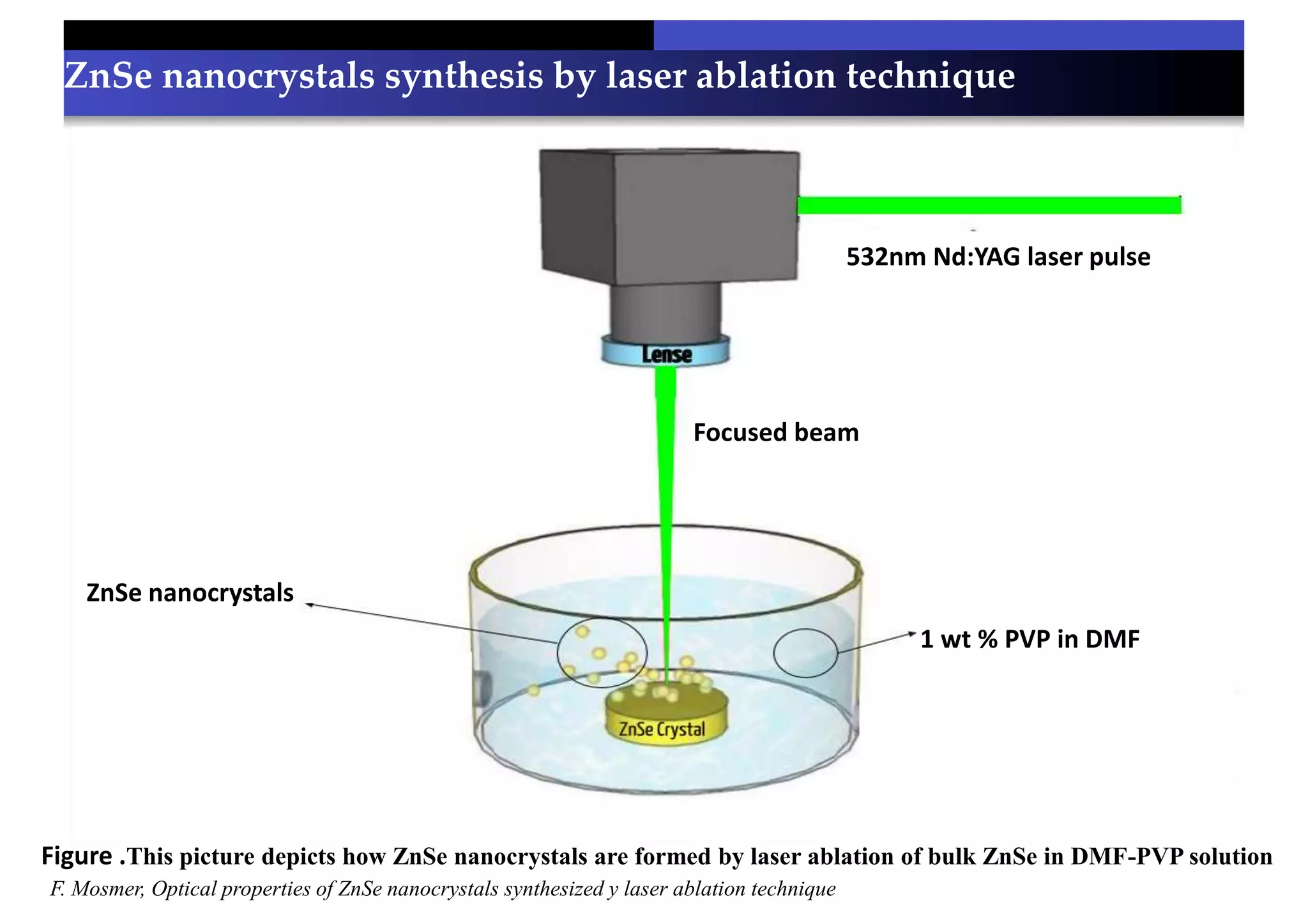
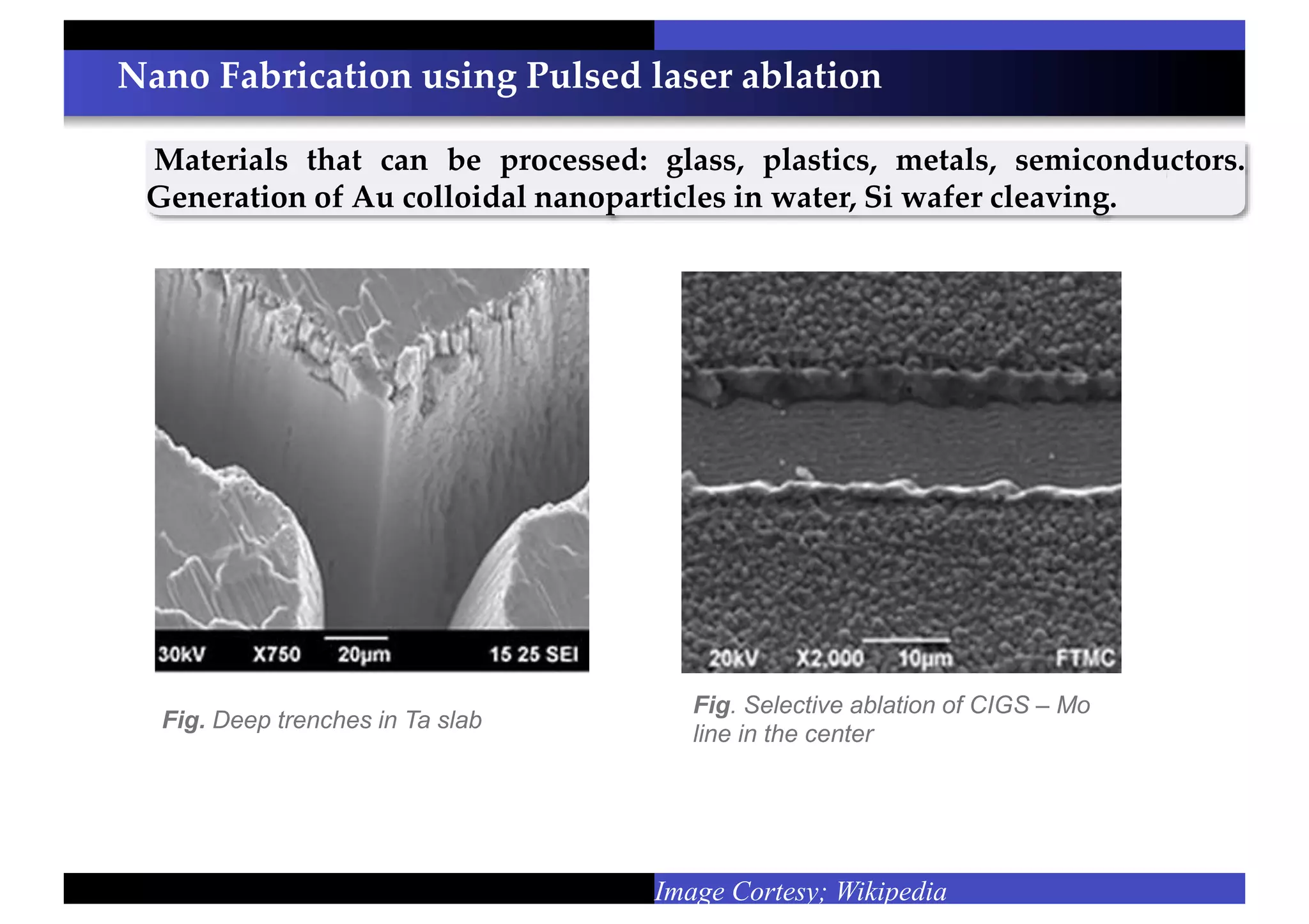
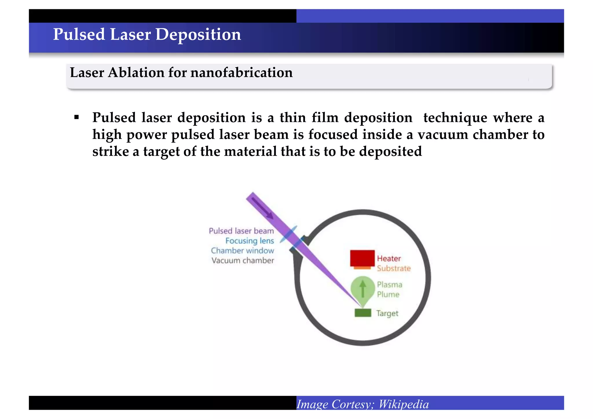
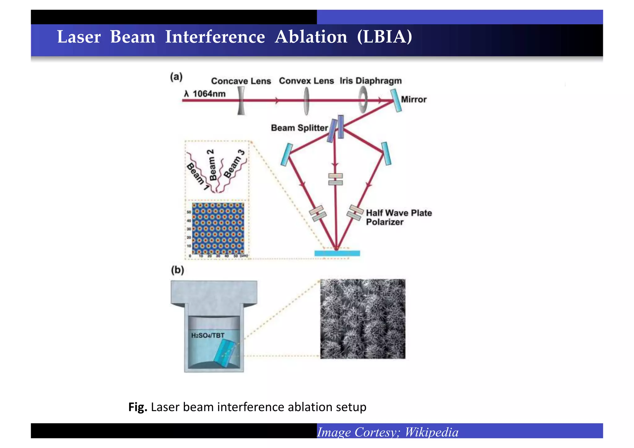
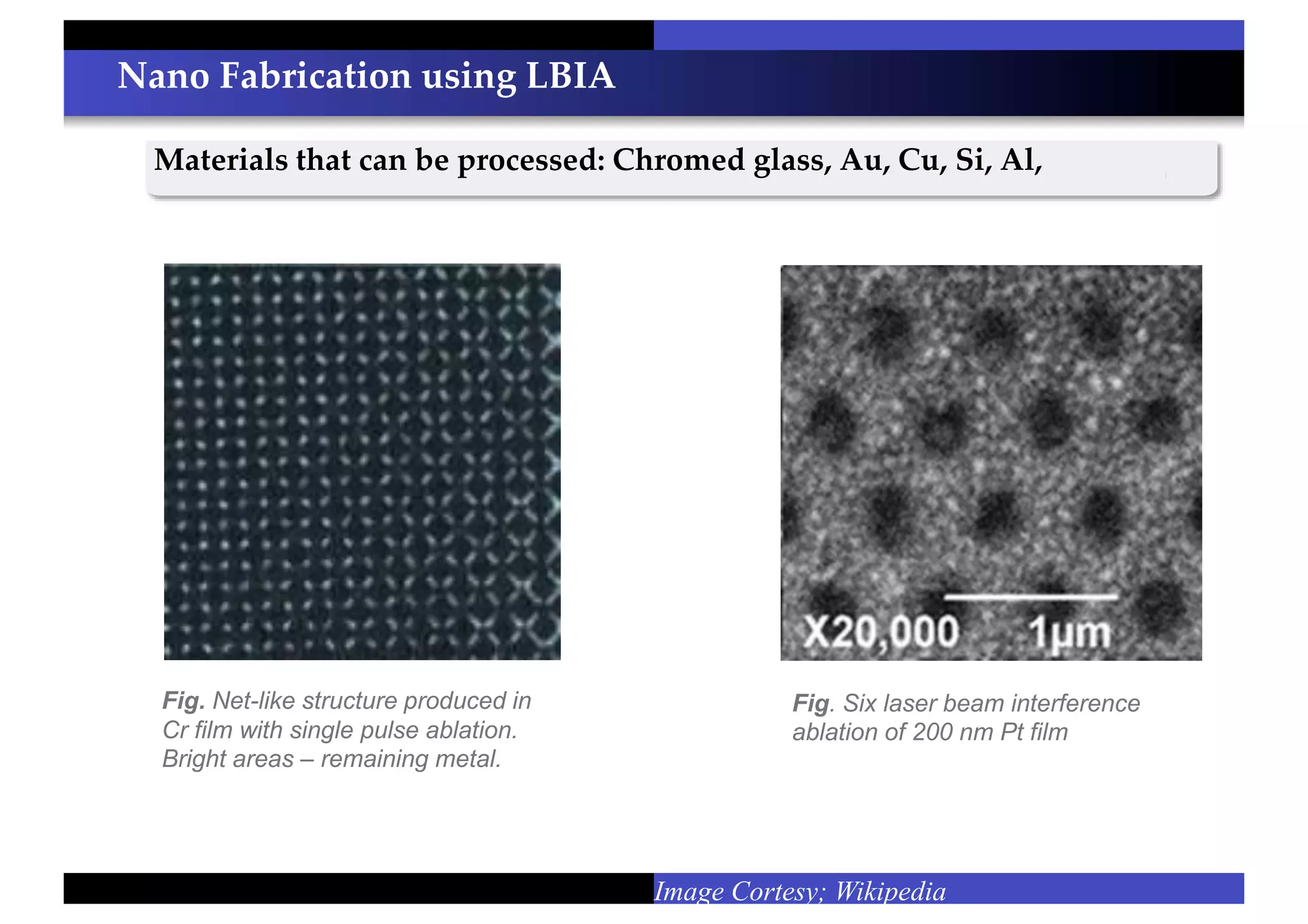
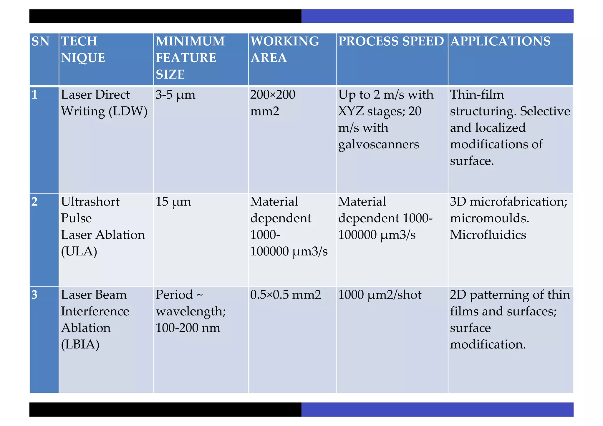
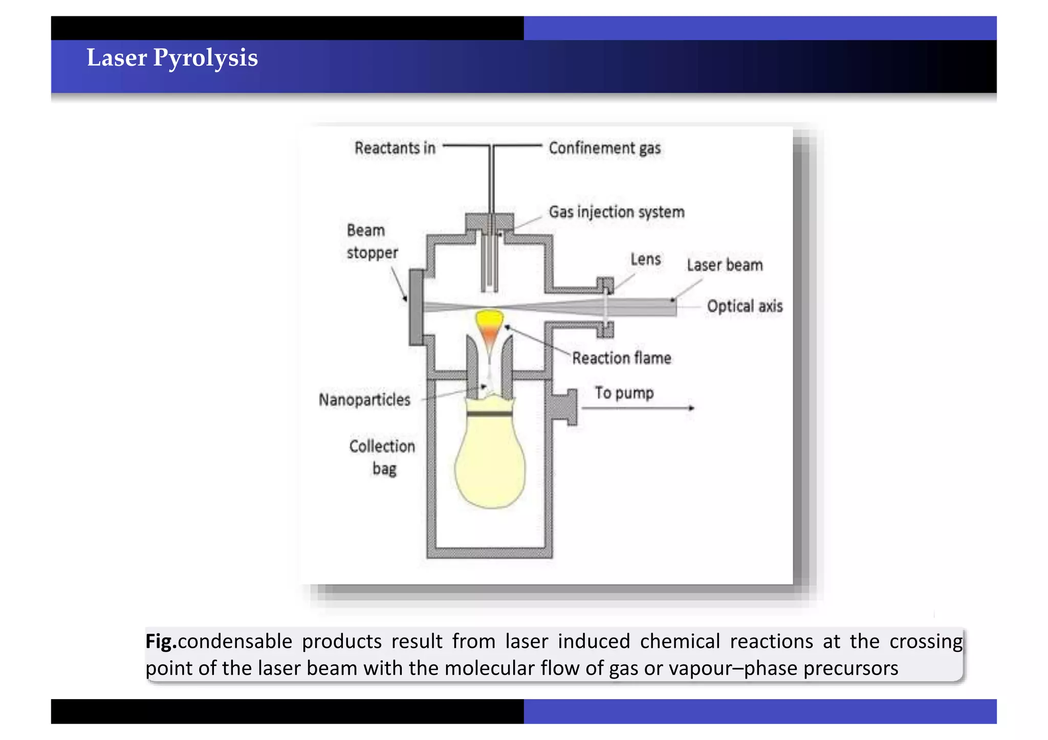
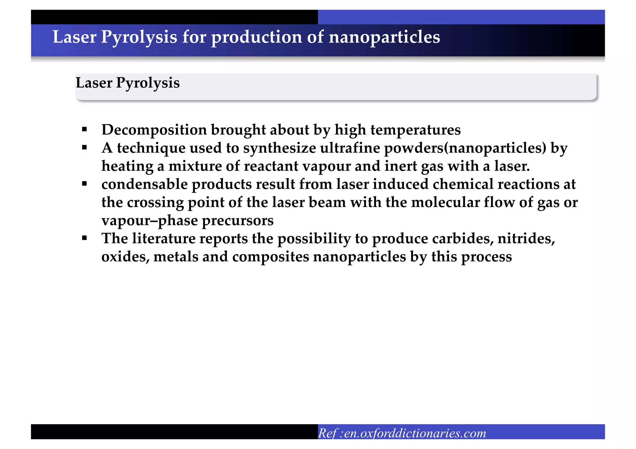
Laser ablation and Pyrolysis
Jaismon Francis
NIT Calicut
Table of content
1. Lasers
1.1 Intensity of Laser radiation
1.2 Different types of lasers and its uses
1.3 Thermal processing of materials using laser
2. Laser ablation
2.1 Cold machining by a continuous wave laser
2.2 Definition of laser ablation
2.3 Laser ablation by a pulsed laser
2.4 Pulsed laser ablation for production of nanoparticles
2.5 Pulsed laser deposition
2.6 Laser beam interference ablation
3. Laser Pyrolysis
3.1 Process of Laser pyrolysis
3.2 Laser pyrolysis for production of nanoparticles
Intensity of Laser Light: Comparison with Sun light
Intensity of
Sunlight at
earth
surface=.105
Watts/𝒄𝒎 𝟐
Intensity of
typical pulsed
laser light is
approximately
10^10
Watts/𝒄𝒎 𝟐
 Laser Light is 100000000000 times intense than Sunlight !!!!
lasers
 Cutting
 Slicing
 Drilling
 Welding
 Surface modification
Laser processing is very mature technology now
 Nd:Yag
 CO2
 Excimer
 Ti:Sapphire
 Cu vapour lasers
Uses of laser in industry Type of lasers used for processing
Conventional laser machining is thermally based processing
Laser light for nano-microfabrication
Thermal processing cause inevitably scorching and rugged edges
Fig. A 25micron trench machined by a laser beam over a 1mm thick Ni-Fe alloy substrate
It will become a critical issue in nanofabrication using lasers
Laser ablation or cold machining by a laser beam
clean cut pattern edge and smooth machined surface
Short wavelength photons from a laser can excite a photochemical reaction
in some macromolecule based materials, which can cause breaking up of
long molecule chains and polymer is directly vaporised without melting
phase
Fig. Examples of polymer microstructures made of direct laser ablation
Laser ablation
Laser Ablation
Image Cortesy; Wikipedia
 Laser ablation or photo ablation is the process of removing material
from a solid (or occasionally liquid) surface by irradiating it with
a laser beam.
Pulsed laser ablation
Ref :oxforddictionaries.com
 A significant development of laser ablation is application of femto
second lasers
 Femtosecond laser is so short when shining on material surface that
laser energy has no time to convert into heat diffusing into adjacent
area
 Material is directly converted from solid state to plasma state and
burst out of surface with out melting
ZnSe nanocrystals synthesis by laser ablation technique
ZnSe nanocrystals
1 wt % PVP in DMF
Focused beam
532nm Nd:YAG laser pulse
Figure .This picture depicts how ZnSe nanocrystals are formed by laser ablation of bulk ZnSe in DMF-PVP solution
F. Mosmer, Optical properties of ZnSe nanocrystals synthesized y laser ablation technique
Nano Fabrication using Pulsed laser ablation
Materials that can be processed: glass, plastics, metals, semiconductors.
Generation of Au colloidal nanoparticles in water, Si wafer cleaving.
Image Cortesy; Wikipedia
Fig. Selective ablation of CIGS – Mo
line in the center
Fig. Deep trenches in Ta slab
Pulsed Laser Deposition
Laser Ablation for nanofabrication
Image Cortesy; Wikipedia
 Pulsed laser deposition is a thin film deposition technique where a
high power pulsed laser beam is focused inside a vacuum chamber to
strike a target of the material that is to be deposited
Laser Beam Interference Ablation (LBIA)
Laser Ablation for nanofabrication
Image Cortesy; Wikipedia
 Laser Beam Interference Ablation (LBIA) combines multiple las
er beams to create a spatial interference pattern. The interference
effect allows reducing feature dimensions to below the diffraction
limit, Multi-beam parallel processing for periodic structures.
 LBIA is used for 2D patterning of thin films and surfaces and
surface modification. Min period 600 nm using 532 nm wavelength,
with uniform spacing within the laser spot size of ~50um
Laser Beam Interference Ablation (LBIA)
Image Cortesy; Wikipedia
Fig. Laser beam interference ablation setup
Nano Fabrication using LBIA
Materials that can be processed: Chromed glass, Au, Cu, Si, Al,
Image Cortesy; Wikipedia
Fig. Net-like structure produced in
Cr film with single pulse ablation.
Bright areas – remaining metal.
Fig. Six laser beam interference
ablation of 200 nm Pt film
SN TECH
NIQUE
MINIMUM
FEATURE
SIZE
WORKING
AREA
PROCESS SPEED APPLICATIONS
1 Laser Direct
Writing (LDW)
3-5 μm 200×200
mm2
Up to 2 m/s with
XYZ stages; 20
m/s with
galvoscanners
Thin-film
structuring. Selective
and localized
modifications of
surface.
2 Ultrashort
Pulse
Laser Ablation
(ULA)
15 μm Material
dependent
1000-
100000 μm3/s
Material
dependent 1000-
100000 μm3/s
3D microfabrication;
micromoulds.
Microfluidics
3 Laser Beam
Interference
Ablation
(LBIA)
Period ~
wavelength;
100-200 nm
0.5×0.5 mm2 1000 μm2/shot 2D patterning of thin
films and surfaces;
surface
modification.
Laser Pyrolysis
Ref :oxforddictionaries.com
 Decomposition brought about by high temperatures
Pyrolysis
Laser Pyrolysis
Fig.condensable products result from laser induced chemical reactions at the crossing
point of the laser beam with the molecular flow of gas or vapour–phase precursors
Laser Pyrolysis for production of nanoparticles
Ref :en.oxforddictionaries.com
Laser Pyrolysis
 Decomposition brought about by high temperatures
 A technique used to synthesize ultrafine powders(nanoparticles) by
heating a mixture of reactant vapour and inert gas with a laser.
 condensable products result from laser induced chemical reactions at
the crossing point of the laser beam with the molecular flow of gas or
vapour–phase precursors
 The literature reports the possibility to produce carbides, nitrides,
oxides, metals and composites nanoparticles by this process
Jaismon Francis
23rd October ,2018
NITC
THANK YOU

laser ablation and pyrolysis for micro machining and nano fabrication

  • 1.
    Laser ablation andPyrolysis Jaismon Francis NIT Calicut
  • 2.
    Table of content 1.Lasers 1.1 Intensity of Laser radiation 1.2 Different types of lasers and its uses 1.3 Thermal processing of materials using laser 2. Laser ablation 2.1 Cold machining by a continuous wave laser 2.2 Definition of laser ablation 2.3 Laser ablation by a pulsed laser 2.4 Pulsed laser ablation for production of nanoparticles 2.5 Pulsed laser deposition 2.6 Laser beam interference ablation 3. Laser Pyrolysis 3.1 Process of Laser pyrolysis 3.2 Laser pyrolysis for production of nanoparticles
  • 3.
    Intensity of LaserLight: Comparison with Sun light Intensity of Sunlight at earth surface=.105 Watts/𝒄𝒎 𝟐 Intensity of typical pulsed laser light is approximately 10^10 Watts/𝒄𝒎 𝟐  Laser Light is 100000000000 times intense than Sunlight !!!!
  • 4.
    lasers  Cutting  Slicing Drilling  Welding  Surface modification Laser processing is very mature technology now  Nd:Yag  CO2  Excimer  Ti:Sapphire  Cu vapour lasers Uses of laser in industry Type of lasers used for processing Conventional laser machining is thermally based processing
  • 5.
    Laser light fornano-microfabrication Thermal processing cause inevitably scorching and rugged edges Fig. A 25micron trench machined by a laser beam over a 1mm thick Ni-Fe alloy substrate It will become a critical issue in nanofabrication using lasers
  • 6.
    Laser ablation orcold machining by a laser beam clean cut pattern edge and smooth machined surface Short wavelength photons from a laser can excite a photochemical reaction in some macromolecule based materials, which can cause breaking up of long molecule chains and polymer is directly vaporised without melting phase Fig. Examples of polymer microstructures made of direct laser ablation
  • 7.
    Laser ablation Laser Ablation ImageCortesy; Wikipedia  Laser ablation or photo ablation is the process of removing material from a solid (or occasionally liquid) surface by irradiating it with a laser beam.
  • 8.
    Pulsed laser ablation Ref:oxforddictionaries.com  A significant development of laser ablation is application of femto second lasers  Femtosecond laser is so short when shining on material surface that laser energy has no time to convert into heat diffusing into adjacent area  Material is directly converted from solid state to plasma state and burst out of surface with out melting
  • 9.
    ZnSe nanocrystals synthesisby laser ablation technique ZnSe nanocrystals 1 wt % PVP in DMF Focused beam 532nm Nd:YAG laser pulse Figure .This picture depicts how ZnSe nanocrystals are formed by laser ablation of bulk ZnSe in DMF-PVP solution F. Mosmer, Optical properties of ZnSe nanocrystals synthesized y laser ablation technique
  • 10.
    Nano Fabrication usingPulsed laser ablation Materials that can be processed: glass, plastics, metals, semiconductors. Generation of Au colloidal nanoparticles in water, Si wafer cleaving. Image Cortesy; Wikipedia Fig. Selective ablation of CIGS – Mo line in the center Fig. Deep trenches in Ta slab
  • 11.
    Pulsed Laser Deposition LaserAblation for nanofabrication Image Cortesy; Wikipedia  Pulsed laser deposition is a thin film deposition technique where a high power pulsed laser beam is focused inside a vacuum chamber to strike a target of the material that is to be deposited
  • 12.
    Laser Beam InterferenceAblation (LBIA) Laser Ablation for nanofabrication Image Cortesy; Wikipedia  Laser Beam Interference Ablation (LBIA) combines multiple las er beams to create a spatial interference pattern. The interference effect allows reducing feature dimensions to below the diffraction limit, Multi-beam parallel processing for periodic structures.  LBIA is used for 2D patterning of thin films and surfaces and surface modification. Min period 600 nm using 532 nm wavelength, with uniform spacing within the laser spot size of ~50um
  • 13.
    Laser Beam InterferenceAblation (LBIA) Image Cortesy; Wikipedia Fig. Laser beam interference ablation setup
  • 14.
    Nano Fabrication usingLBIA Materials that can be processed: Chromed glass, Au, Cu, Si, Al, Image Cortesy; Wikipedia Fig. Net-like structure produced in Cr film with single pulse ablation. Bright areas – remaining metal. Fig. Six laser beam interference ablation of 200 nm Pt film
  • 15.
    SN TECH NIQUE MINIMUM FEATURE SIZE WORKING AREA PROCESS SPEEDAPPLICATIONS 1 Laser Direct Writing (LDW) 3-5 μm 200×200 mm2 Up to 2 m/s with XYZ stages; 20 m/s with galvoscanners Thin-film structuring. Selective and localized modifications of surface. 2 Ultrashort Pulse Laser Ablation (ULA) 15 μm Material dependent 1000- 100000 μm3/s Material dependent 1000- 100000 μm3/s 3D microfabrication; micromoulds. Microfluidics 3 Laser Beam Interference Ablation (LBIA) Period ~ wavelength; 100-200 nm 0.5×0.5 mm2 1000 μm2/shot 2D patterning of thin films and surfaces; surface modification.
  • 16.
    Laser Pyrolysis Ref :oxforddictionaries.com Decomposition brought about by high temperatures Pyrolysis
  • 17.
    Laser Pyrolysis Fig.condensable productsresult from laser induced chemical reactions at the crossing point of the laser beam with the molecular flow of gas or vapour–phase precursors
  • 18.
    Laser Pyrolysis forproduction of nanoparticles Ref :en.oxforddictionaries.com Laser Pyrolysis  Decomposition brought about by high temperatures  A technique used to synthesize ultrafine powders(nanoparticles) by heating a mixture of reactant vapour and inert gas with a laser.  condensable products result from laser induced chemical reactions at the crossing point of the laser beam with the molecular flow of gas or vapour–phase precursors  The literature reports the possibility to produce carbides, nitrides, oxides, metals and composites nanoparticles by this process
  • 19.
    Jaismon Francis 23rd October,2018 NITC THANK YOU

Editor's Notes

  • #2 Good afternoon Particularly application of these into micro and nanofabrication
  • #3 1.In electronics and mechanical industries 2.Lasers used for material processing includes 3.Laser beam of of high energy density generates highly localized heating on a work piece causing material to melt and vaporis
  • #4 To get a feel 100 billion
  • #5 1.In electronics and mechanical industries 2.Lasers used for material processing includes 3.Laser beam of of high energy density generates highly localized heating on a work piece causing material to melt and vaporis
  • #6 1.Edge roughfenning due to melting and deposition of debris also visible 2.For big work pieces microscale roughening is not a problem
  • #7 1.Cold micro machining can avoid scorching and melting
  • #9 1.Conventional ss lasers have pulsewidth in the order of nanoseconds 2.Laser falls on a material it can trigger a multude of physical and chemical changes to the material 3. The ejected species from solid surface expand into surrounding medium in the form of a plume containing many energetic species including atoms, molecules, electron, clusters 4.Its a cold process clean cut edge
  • #10 diggression It is simple and clean synthesis There is no need to further purification and use of matrices and ligands to prevent agglomeration. Size distribution and morphology of synthesized nanocrystals can be controlled by changing parameters such as wavelength ,laser beam fluence, pulse energy ,pulse duration and frequency of pulsed laser
  • #18 If the molecules are excited above the dissociation threshold, molecular decomposition, eventually followed by chemical reactions, occurs with the formation of condensable and/or volatile products 2. Nucleation and growth of nanoparticles occurs in a very short time by coagulation and coalescence of the reaction products and the growth is abruptly terminated as soon as the particles leave the irradiation region. As a result, nanoparticles with average size ranging from 5 to 30 nm and narrow size distribution are formed in the hot region