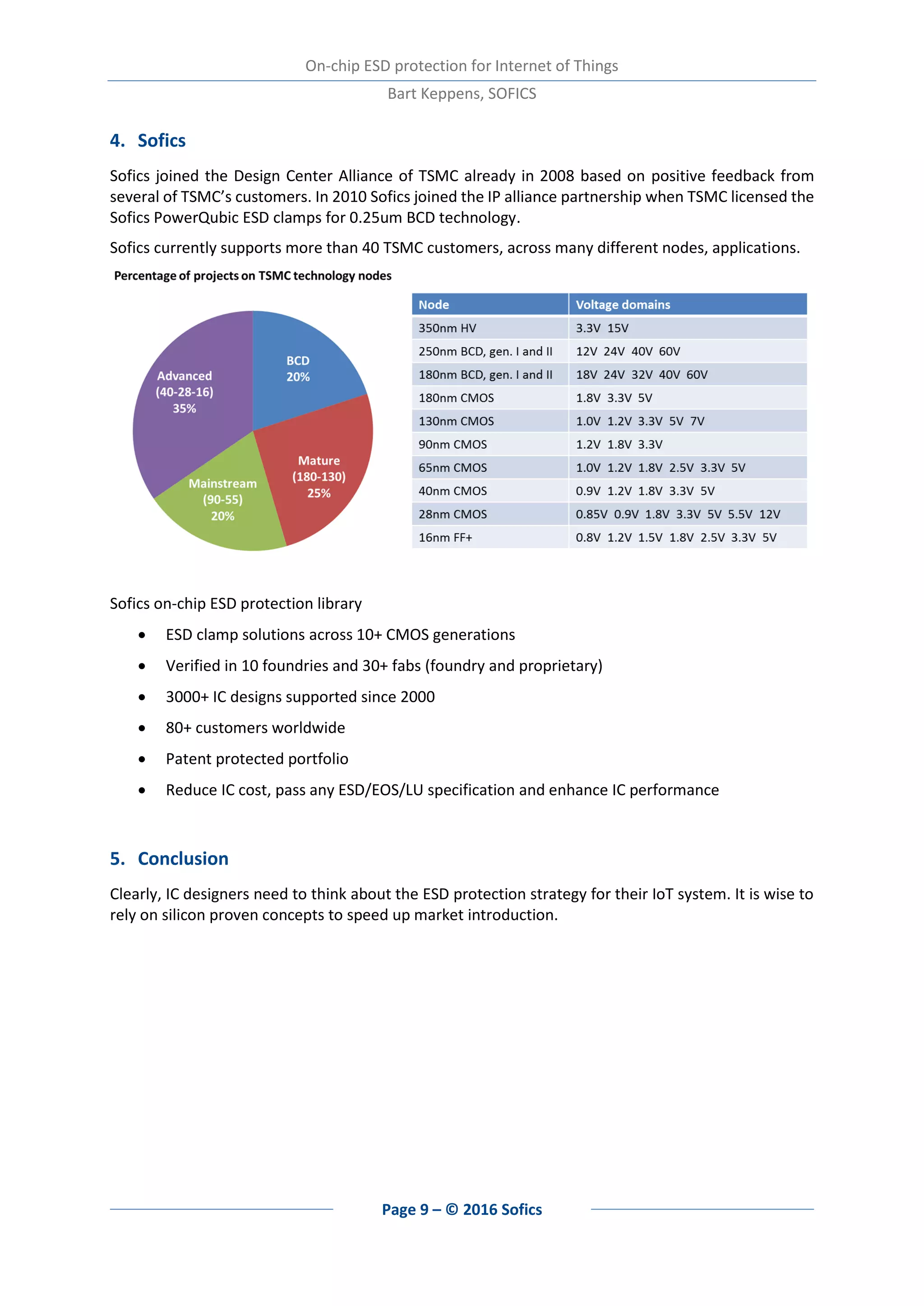
Many of the applications in Internet of Things require non-standard on-chip ESD protection clamps. We identified 5 reasons.
- Non-standard signal voltages
- Low leakage requirement
- Sub-systems are powered down
- Wireless interfaces
- System level protection, on the chip
Clearly, IC designers need to think about the ESD protection strategy for their IoT system. It is wise to rely on silicon proven concepts to speed up market introduction.
White paper on ESD protection for 40nm/28nmbart_keppens
40/28nm ESD approach
On-chip ESD protection clamps for advanced 40nm and 28nm CMOS technology
Despite the rising cost for IC development, EDA tools and mask sets semiconductor design companies continue to use the most advanced CMOS technology for high performance applications because benefits like lower power dissipation, increased gate density, higher speed and lower manufacturing cost per die more than compensate the higher cost.
This return on investment however only pays off for ultra high volume applications. Due to the use of sensitive elements (such as ultra thin-oxide transistors, ultra-shallow junctions, narrow and thin metal layers), increased complexity through multiple voltage domains and the use of IP blocks from various vendors, a comprehensive ESD protection strategy becomes more important.
This white paper presents on-chip ESD protection clamps and approaches for 40/28nm CMOS that provide competitive advantage by improved yield, reduced silicon footprint and enable advanced multimedia and wireless interfaces like HDMI, USB 3.0, SATA, WiFi, GPS and Bluetooth. The solutions are validated in tens of products running in foundry and proprietary fabrication plants.
On-chip ESD protection for Silicon PhotonicsSofics
In the past, Fiber-optic communication was used only for long distance communication (50 km and beyond). Only a limited number of these high-end interface products were required worldwide. More recently, companies running large data centers (Facebook, Google, Amazon,...) like to replace the traditional cabling between server racks. The copper-based approach is considered a bottleneck for further improvements in data transfer capacity. Optical fiber can dramatically increase the bandwidth between servers and reduce complexity.
Thus, the optical interconnect suppliers now need to produce a large number of their products. To reduce the cost, they separate the optical parts (laser diodes, photo detectors) from the digital controller circuits. That allows to rely on advanced, standard CMOS technology for those controller circuits, enabling a cost-effective high-volume production. Both elements are combined within a single IC package using advanced packing techniques.
The 25-56Gbps interfaces consist of SerDes-type circuits and are integrated into advanced CMOS technology like 28nm CMOS. To create such high-speed differential I/O circuits, designers utilize the thin oxide transistors. However, those transistors are very sensitive and can be easily damaged during transient events like electrostatic discharge (ESD).
Despite the fact that the sensitive pads are not connected outside of the package, they could still receive ESD stress during assembly. Therefore, adequate protection clamps need to be inserted at the bond pads. On the other hand, for signal integrity, it is important to limit the capacitance between the interface pads and the supply lines.
Sofics has worked with several companies developing these optical interconnect interfaces. Sofics developed ESD protection with parasitic capacitance below 15fF, ten times lower than the typical low-cap ESD protection devices in TSMC 28nm CMOS.
IoT workshop - Is 1kV Also Enough for IoT ESD Protection – Do Current Test Me...Sofics
Integrated Circuits designed for Internet of Things (IoT) applications require special attention with respect to ESD and EOS protection. Because of the form factor the Transient Voltage Suppressors are typically left out while the probability to receive stress increases. In this work we summarize the usefulness of current ESD standards for several IoT case studies.
Presentation at the 2018 IoT workshop by Sofics' CEO Koen Verhaege
A leading company, HZO features as the cover of this
edition. HZO, the leader in protecting electronics from the
most demanding environments with world class nano
coatings to enable a better, more durable product
recognized that the available protection options (seals,
gaskets, heavy & thick conformal coatings) had significant
drawbacks, especially for this new generation of
electronics.
A durable and flexible display with low-power consumption, high-contrast ratio, has been a technical challenge for years. They have to be lightweight, rugged, and in some cases, conformal, wearable, rollable and unbreakable. The recent successful integration of flexible display technologies and the traditional web-based processing and/or inkjet technologies has opened up the possibility of low cost and high throughput roll-to-roll manufacturing and has shown the potential to replace the paper used today.
3D Integrated Circuits and their economic feasibilityJeffrey Funk
These slides use concepts from my (Jeff Funk) course entitled analyzing hi-tech opportunities to analyze how the economic feasibility of 3D integrated circuits (ICs) is becoming better and this will enable the continuation of Moore’s Law. 3D ICs involve the stacking of transistors and memory cells on top of each other in order to increase the number of transistors per chip area and thus continue Moore’s Law. As opposed to attempting to further reduce the feature sizes, engineers build up. They increase the number of layers of transistors and memory cells just as they have increased the number of layers of metal interconnect. To do this, they connect the different layers of transistors and memory cells with so-called Vias that are fabricated from copper.
IC suppliers began shipping 3D ICs in 2006 and these shipments have gradually grown and expanded from simple structured ICs such as image sensors to power ICs, and more recently memories, microprocessors, and ASICs. It is easier to increase the number of layers on simple than complex structured ICs. The global 3D IC market is expected to grow from $2.21 billion in 2009 to $6.55 billion in 2016 at a compound annual rate of 16.9% from 2011 to 2016.
Although it is hard to compare actual 2D and 3D ICs, simulations allow us to easily do such comparisons. For example, simulations found that chip area is almost 50% less and the metal length is about 28% less for 3D than 2D chips. The shorter metal length means that speeds will be faster since the electrons have less distance to travel. Simulations show that timing delay is 37%, 57% and 65% shorter for 2, 3, and 4-layer 3D ICs, data transfer rates are faster, and operating frequency is about 30% fasters for 3D than 2D ICs. Simulations also show that power consumption is lower for 3D ICs, achieving a 40% reduction with 4-layer 3D ICs as compared to 2D ICs.
Perhaps more importantly, these simulations show that 3D ICs are theoretically cheaper to develop and manufacture. The reason is that 3D ICs can use larger feature sizes than can 2D ICs in order to achieve the same densities of transistors per chip. These larger feature sizes reduce the cost of equipment such as photolithographic equipment, whose costs are rising rapidly. Simulations show that capital costs for 3D ICs are 5% and R&D costs are those of 2D ICs. For manufacturing costs, simulations of flash memory that the advantage of 3D ICs increases as the size of flash memory increases reaching 50% with 256Gb.
All of this suggests that Moore’s Law will continue for many years. Combined with the reductions in feature size that were mentioned earlier from International Technology Roadmap for Semiconductors, there is probably another 10-20 years left in Moore’s Law just from 3D ICs and smaller feature sizes. Nevertheless, challenges remain for 3D ICs. The simulations assume similar yields when in reality it will be harder to achieve similar yields on 3D as 2D ICs given the increa
Using Nanocoatings: Opportunities & Challenges for Medical DevicesCheryl Tulkoff
There is significant opportunity for improvements in contamination prevention, field performance and cost of medical devices through the use of biocompatible nanocoatings. To be successful using these coatings requires knowledge of the materials and processes on the market, the regulatory status, and the benefits versus risks.
This presentation will provide a clear understanding of the current state of nanocoating technology for medical devices and electronics. There has been an explosion in new coating technologies over the past 24 months. The use of nanocoatings has been driven by the desire for moisture proofing, providing an oxygen barrier ( a hermeticity option) and mitigating tin whiskers. Successful adoption of these coating technologies can lead to improved performance and market differentiation. Inappropriate adoption can drive higher failure rates, recalls and alienation of customers. Obtaining relevant reliability and quality information can be difficult. The information is often segmented for different markets; and, the focus is on the opportunities, not the risks. The primary information sources are either marketing material or confusing, scientific studies. Where is the practical advice?
3-D ICs are an attractive chip architecture that can alleviate the interconnect related problems such as delay and power dissipation and can also facilitate integration of heterogeneous technologies in one chip (SoC).
Here following we will discuss about their classification according to the configuration and in another article we will discuss their classification according to application and colours code.
2019 Local I/O ESD protection for 28Gbps to 112Gbps SerDes interfaces in adva...Sofics
2019 Taiwan ESD and reliability conference
Semiconductor companies are developing ever faster wireless, wired and optical interfaces to satisfy the need for higher data throughputs. They rely on BiCMOS, advanced CMOS and FinFET nodes with ESD-sensitive circuits. However, the parasitic capacitance of the traditional ESD solutions limits the signal frequency. This paper demonstrates small area and low-cap Analog I/Os used in TSMC 28nm CMOS and TSMC 16nm, 12nm, 7nm FinFET technologies for high speed SerDes (28Gbps to 112Gbps) circuits. Parasitic capacitance of the ESD solutions is reduced below 100fF and for some silicon photonics applications even below 20fF.
2011 ESD relevant issues and solutions for overvoltage tolerant, hot swap, op...Sofics
2011 Taiwan ESD and Reliability conference
The ‘Dual diode’ approach is one of the most used on-chip and off-chip concept for ESD protection of IO interfaces. It is simple to implement, smaller than any other IO/ESD concept, has a low parasitic capacitance and low leakage. However, especially the ‘diode up’, from IO-pad to VDD can create a lot of problems in the functional operation of the circuits. This paper summarizes a number of problems that are caused by the ‘diode up’, describes the differences between overvoltage tolerant, hot swap, open drain and failsafe interface concepts and provides solutions that can solve both functional operation and ESD.
Optimized Local I/O ESD Protection for SerDes In Advanced SOI, BiCMOS and Fin...Sofics
Sofics presentation (B2.2) at the 1st International EOS/ESD Symposium on Design and System (IEDS). IEDS is dedicated to the fundamental understanding of issues related to electrostatic discharge on design and system and the application of this knowledge to the solution of problems.
Semiconductor companies are developing ever faster interfaces to satisfy the need for higher data throughputs. However, the parasitic capacitance of the traditional ESD solutions limits the signal frequency. This paper demonstrates low-cap Analog I/Os for high speed SerDes (28Gbps to 112Gbps) circuits created in advanced BiCMOS, SOI and FinFET nodes.
2010 The Hebistor Device: Novel latch-up immune ESD Protection Clamp for High...Sofics
2010 Taiwan ESD and reliability conference
High voltage interfaces are broadly used in many IC applications like motor control, power management and conversion, LCD panel drivers and automotive systems. Because the high voltage IC's are typically used in severe applications IC designers need to protect their circuits to a steady growing list of requirements. In this paper we present an overview of the ESD, EOS and latch‐up requirements and compare the performance of different on‐chip ESD protection approaches. The paper introduces a newly developed protection device with a high holding voltage for absolute latch‐up immunity.
2011 Latch-up immune ESD Protection Clamp for High Voltage optimized on TSMC ...Sofics
2011 TSMC open innovation Platform
Applications like motor control, power management and conversion, LCD panel drivers and automotive systems require IC interfaces that can tolerate and drive high voltages (10V to 100V). Moreover, in most of these applications the ICs are operated in harsh environments (high temperature, high current/voltage transient disturbance), close to the boundaries of the IC technology. Further, to reduce the Bill of Materials (BOM) system makers are constantly shifting requirements that were once a system/PCB issue to the IC makers. IC makers designing high voltage applications need robust and reliable technology that can meet a growing set of requirements.
Based on TSMC’s comprehensive BCD technology platform in 0.25um and 0.18um, Sofics has developed novel EOS/ESD protection devices that can solve those needs.
This paper first presents an overview of the EOS, ESD, latch-up and other requirements that IC makers face today. Secondly the TSMC BCD technology that was used as the verification platform is touched upon. Finally analysis results and on-going product implementations are shown on 0.25um BCD and 0.18um BCD technology. The unique BCD ESD solutions are available for TSMC foundry customers at a fraction of the development cost.
On-Chip ESD Protection Achieving 8kV HBM Without Compromising the 3.4Gbps HDM...Sofics
To maintain signal integrity on HDMI TMDS interfaces ESD protection requires careful design. Moreover, due to direct consumer interaction higher ESD specifications are requested. This paper presents results for an HDMI circuit achieving 8kV HBM without compromising the 3.4Gbps data rate through the use of low capacitive on‐chip ESD clamps.
Sofics hebistor clamps
Latch-up Immune on-chip ESD protection for High Voltage processes and applications
While high voltage interfaces are broadly used in many IC applications like motor control, power management and conversion, LCD panel drivers and automotive systems, many IC designers still lack a low leakage, costeffective and latch-up immune ESD protection clamp that can be applied across various applications.
The behavior of many of the traditional on-chip ESD clamps is tied to the process conditions, which limits the possibilities to adapt to changing specifications. Moreover, severe reliability requirements that were long requested only for industrial and automotive applications are now being transferred to consumer electronics too.
This white paper introduces a new family of ESD/EOS/IEC protection devices, called hebistor clamps that provide competitive advantage through improved yield, reduced silicon footprint and low leakage operation. The hebistor devices are developed to protect a broad set of high voltage interfaces in BCD and high voltage CMOS and are branded under the Sofics PowerQubic portfolio. Based on measurements on TSMC 0.35um 15V and TSMC 0.25um BCD 12V, 24V, 40V and 60V technology the flexibility of the novel device is demonstrated.
Smart thermostats provide connected households with a convenient way to increase energy efficiency through the Internet of Things. Littelfuse offers a broad portfolio of products for smart thermostats that protect, control, and sense.
1.2V core power clamp for TSMC 65nm technologySofics
Sofics has verified its TakeCharge ESD protection clamps on technology nodes between 0.25um CMOS down to 5nm across various fabs and foundries. The ESD clamps are silicon and product proven in more than 4500 mass produced IC-products. The cells provide competitive advantage through improved yield, reduced silicon footprint and enable advanced multimedia and wireless interfaces like HDMI, USB 3.0, SATA, WIFI, GPS and Bluetooth.
The ESD clamp described in this document protects 1.2V core domains in TSMC 65nm CMOS technology.
Littelfuse Solutions for Security Cameras and Video DoorbellsLittelfuse
Smart homes are equipped with intelligent technologies for convenient and energy-efficient living. View the benefits of Littelfuse products that provide protection and control for security camera and video doorbell applications.
Building Automation,Networking & Communication Presentation by LVS 2022.pdfMahesh Chandra Manav
Link Vue System Offering Technical and Genuine support to all Customers also Introducing of New Technologies upgradation knowledge of customer while preparing Tenders for New and Modernization of Old facilities .
We are into OEM for Networking Products LAN ,Fiber Optics and Wireless with GSM Solutions. Electrical Connectors ,PLUG Sockets and Electric Vehicles Cable Harness, We are also distributor of Surge Protection and System Integrators of Building ,Automation , Smart Data Loggers, Protocol Convertors, Protocol to FO Convertors, CCTV , Fire Alarm , Access Controls, Security Systems, Audio Visuals ,PA Systems , EPABX ,Parking Managements and Enterprises Solutions with PIDS Fencing.
Latest We Introduce DRONE Survey and Monitoring Services, Weather Monitoring Station and Electric Vehicle Charging Unit for AC and DC Charging of Electric Vehicles 3KW-360KW.
We are into Design Engineering Selection of Right and Genuine Components as per application and Environment demand with Installation by Professionals.
to know more plz visit our webpage www.linkvuesystem.com
Mahesh Chandra Manav HOD M-9811247237 manav.chandra@linkvuesystem.com
you can visit my profile and comments
Design of ESD protection for high-speed interfacesSofics
Semiconductor companies are developing ever faster wireless, wired and optical interfaces to satisfy the need for higher data throughputs. They rely on BiCMOS, advanced CMOS and FinFET nodes with ESD-sensitive circuits. However, the parasitic capacitance of the traditional ESD solutions limits the signal frequency. This paper demonstrates small area and low-cap Analog I/Os used in TSMC 28nm CMOS and TSMC 16nm, 12nm, 7nm FinFET technologies for high speed SerDes (28Gbps to 112Gbps) circuits. Parasitic capacitance of the ESD solutions is reduced below 100fF and for some silicon photonics applications even below 20fF.
2020 04 sofics low cap esd
Nowadays, mobile consumer electronics devices integrate various wireless interfaces like WIFI, Bluetooth, GPRS and GPS. Various approaches exist to protect the wireless interfaces against ESD stress. In recent years, researchers have focused on so‐called 'co‐design' techniques to solve both functional and protection constraints together which requires both RF and ESD design skills. However many IC designers still prefer to work with 'plug‐n‐play' protection concepts where the ESD clamps exhibit low parasitic capacitance, low series resistance and low leakage. This paper presents measurement results of 3 different SCR based protection approaches that exhibit high Q‐factor and low and stable parasitic capacitance over a broad voltage and frequency range. The clamps are used for protection of LNA circuits in 90nm and 40nm Low Power (LP) CMOS technologies.
Littelfuse Battery Fuel Gauge and I/O Port Protection SolutionsLittelfuse
Battery fuel gauge ICs are used in many consumer electronics and appliance applications. View the variety and benefits of Littelfuse solutions available for your application.
Similar to On chip esd protection for Internet of Things (20)
Tsmc65 1v2 full local protection analog io + cdmSofics
Sofics has verified its TakeCharge ESD protection clamps on technology nodes between 0.25um CMOS down to 5nm across various fabs and foundries. The ESD clamps are silicon and product proven in more than 4500 mass produced IC-products. The cells provide competitive advantage through improved yield, reduced silicon footprint and enable advanced multimedia and wireless interfaces like HDMI, USB 3.0, SATA, WIFI, GPS and Bluetooth.
The Analog I/O clamp described in this document can be used for 1.2V pads in the TSMC 65nm CMOS technology. It has a full local ESD protection and integrated power clamp. The bus resistance is thus not important for IO related ESD stress.
The cell also includes a CDM secondary protection.
1.2V Analog I/O with full local ESD protection for TSMC 65nm technologySofics
Sofics has verified its TakeCharge ESD protection clamps on technology nodes between 0.25um CMOS down to 5nm across various fabs and foundries. The ESD clamps are silicon and product proven in more than 4500 mass produced IC-products. The cells provide competitive advantage through improved yield, reduced silicon footprint and enable advanced multimedia and wireless interfaces like HDMI, USB 3.0, SATA, WIFI, GPS and Bluetooth.
The Analog I/O clamp described in this document can be used for 1.2V pads in the TSMC 65nm CMOS technology. It has a full local ESD protection and integrated power clamp. The bus resistance is thus not important for IO related ESD stress.
1.2V Over-voltage tolerant Analog I/O for TSMC 65nm technologySofics
Sofics has verified its TakeCharge ESD protection clamps on technology nodes between 0.25um CMOS down to 5nm across various fabs and foundries. The ESD clamps are silicon and product proven in more than 4500 mass produced IC-products. The cells provide competitive advantage through improved yield, reduced silicon footprint and enable advanced multimedia and wireless interfaces like HDMI, USB 3.0, SATA, WIFI, GPS and Bluetooth.
The Analog I/O clamp described in this document can be used for 1.2V pads in the TSMC 65nm CMOS technology. It is over-voltage tolerant, suitable for hot-swap, cold-spare, open-drain interfaces.
1.2V Analog I/O library for TSMC 65nm technologySofics
Sofics has verified its TakeCharge ESD protection clamps on technology nodes between 0.25um CMOS down to 5nm across various fabs and foundries. The ESD clamps are silicon and product proven in more than 4500 mass produced IC-products. The cells provide competitive advantage through improved yield, reduced silicon footprint and enable advanced multimedia and wireless interfaces like HDMI, USB 3.0, SATA, WIFI, GPS and Bluetooth.
2011 Protection of a 3.3V Domain and Switchable 1.8V/3.3V I/O in 40nm and 28n...Sofics
2011 Japan RCJ symposium
Today’s advanced technologies’ overdrive transistors cannot always meet the signal speeds of existing standards. This paper describes the issues, solutions and results to build the necessary protection for HBM, MM, CDM and latch-up for a 3.3V domain and 1.8V/3.3V I/O, based only on 1.8V transistors, in a 40nm process. Results of the design ported to 28nm are also presented.
2012 The impact of a decade of Technology downscalingSofics
2012 Taiwan ESD and reliability conference
Over a decade the technology is decreased from 0.18um to below 28nm, which affects not only the technology parameters but also the ESD performance. Due to further downscaling implementation becomes more difficult to meet the normal operation requirements (area, leakage…). The most important trends are summarized in this paper.
2012 Protection strategy for EOS (IEC 61000-4-5)Sofics
2012 Taiwan ESD and reliability conference
The standard IEC 61000-4-5 is used to characterize IC designs for EOS robustness. Each chip should achieve a minimum level of protection to withstand against EOS. Based on Long TLP and simulation, a strategy is developed to handle this requirement. The methodology has been applied for a T-con product in 130nm CMOS.
2012 Unexpected failures due to dynamic avalanching caused by bipolar ESD stressSofics
2012 Taiwan ESD and reliability conference
The bipolar nature of ESD pulses such as MM introduces failure mechanisms that cannot be reproduced by TLP/HBM. A lowered breakdown voltage due to dynamic avalanching was observed. The key issue is that carriers injected during the first swing remain in the device after the current switches polarity. A case study for high-voltage diodes is presented.
2017 EOS/ESD symposium
This paper presents a novel approach to reduce the parasitic capacitive loading of RF and high speed digital interfaces by up to 35%. Unlike in the classic dual diode protection, both junctions connected to the pad are used in every stress combination.
ESD protection with ultra-low parasitic capacitance for high bandwidth commun...Sofics
The ever increasing demand to transfer data pushes the semiconductor industry to develop faster wired, wireless or optical interfaces (>20 Gbps).
To meet those speeds, chip designers need to limit the parasitic capacitance of the on-chip ESD protection clamps. When traditional ESD concepts are not good enough, they need special analog I/O circuits like the proprietary solutions made available by Sofics.
Sofics is a foundry independent semiconductor IP company providing custom, specialty analog I/Os and on-chip ESD protection.
Our technology is characterized on 10 foundries including advanced nodes at TSMC, UMC, GF, TowerJazz. Our silicon design and circuit solutions are complementary to the public and foundry solutions
Sofics has silicon proven Analog I/O’s & ESD clamps on advanced FinFET processes including 16nm, 12nm & 7nm. Several companies have integrated Sofics IP in their SoCs.
Proven technology gives you first time right designs
Sofics ESD technology has been included in 4500+ mass-produced IC designs, corresponding to millions of wafers. The solutions have successfully been transferred to advanced CMOS and FinFET technology nodes.
Broad solution spectrum gives you more options
Sofics has ESD solutions for the different power domains and for every type of interface. The clamps are used in Analog I/O’s and can be used to protect digital I/O’s. The technology can be easily customized to fit various requirements.
Beyond standard performance boosts your competitive advantage
Sofics creates ESD clamps with ultra-low parasitic capacitance for high speed interfaces like 112Gbps. Clamps can be scaled to high ESD robustness like 8kV HBM. Sofics solutions add low stand-by leakage and if needed can tolerate a higher voltage.
Local I/O ESD protection for 28Gbps to 112Gbps SerDes interfaces in advanced ...Sofics
Presentation at the Taiwan ESD and reliability conference 2019
Semiconductor companies are developing ever faster wireless, wired and optical interfaces to satisfy the need for higher data throughputs. They rely on BiCMOS, advanced CMOS and FinFET nodes with ESD-sensitive circuits. However, the parasitic capacitance of the traditional ESD solutions limits the signal frequency. This paper demonstrates small area and low-cap Analog I/Os used in TSMC 28nm CMOS and TSMC 16nm, 12nm, 7nm FinFET technologies for high speed SerDes (28Gbps to 112Gbps) circuits. Parasitic capacitance of the ESD solutions is reduced below 100fF and for some silicon photonics applications even below 20fF.
Optimization of On-chip ESD protection with ultra-low parasitic capacitance t...Sofics
Optimization of On-chip ESD protection with ultra-low parasitic capacitance through Calibre PEX
Johan Van der Borght presented at the 2017 User-to-User conference of Mentor Graphics in Munich.
He talked about our approach to deliver ESD protection with ultra-low parasitic capacitance
Developing robust, 5V tolerant analog I/O libraries for CMOS processes & FinF...Sofics
Presentation by Vera on the Mentor Graphics technology day in Cambridge (2018-09-11). In the presentation Vera covered different topics including techniques used at Sofics to speed up design. She also presented solutions for 5V tolerant interfaces and protection of high speed interfaces against ESD stress
Optimizing I/O’s and ESD protection to reduce power consumption in SOI applic...Sofics
Sofics presentation at the virtual event about FD-SOI, organized by Design&Reuse the day before DATE 2020.
Optimizing I/O’s and ESD protection to reduce power consumption in SOI applications
Sofics' CTO, Benjamin Van Camp explains the different sources for leakage by ESD devices, specifically targeted on SOI applications. He used experimental data from several SOI projects
On-Chip ESD Protection with Improved High Holding Current SCR (HHISCR) Achiev...Sofics
For the design of on‐chip ESD clamps against system level ESD stress three main challenges exist: reach a high failure current, ensure latch‐up immunity and limit transient overshoots. Bearing these in mind, high system level ESD requirements should be within reach. A novel improved high holding current SCR is introduced fulfilling all three requirements within drastically reduced silicon area.
Patented solution to improve ESD robustness of SOI MOS transistorsSofics
Multi‐finger SOI MOS devices exhibit a low ESD failure current, related to the thin Si‐film and the complete isolation of the transistor body regions, causing non ]uniform conduction in bipolar snapback mode. The traditional layout approaches (silicide blocked junctions, increased gate length) are compared and a novel layout concept is proposed to improve uniform triggering.
Excellent ESD performance around 3mA/um2 is achieved for minimum dimension, fully silicided devices in a 90nm SOI technology.
Patented way to create Silicon Controlled Rectifiers in SOI technology Sofics
This paper introduces an SCR based ESD protection design for SOI technologies. It is explained how efficient SCR devices can be constructed in SOI. These devices outperform MOS devices by about 4 times.
Experimental data from 65nm and 130nm SOI is presented to support this.
Introduction to TakeCharge on-chip ESD solutions from SoficsSofics
TakeCharge is a semiconductor Intellectual Property (IP) portfolio that is used by 70+ IC design companies worldwide to protect integrated Circuit (IC) interfaces against ESD stress.
The portfolio includes various ESD clamps, concepts that reduce IC cost, enable high end applications and can protect against severe EOS/ESD constraints.
The presentation includes several examples
- Low leakage on-chip ESD clamps (10 nA range)
- Low parasitic capacitance (150fF range)
- Easily ported to any CMOS node
- Reduce development cost and time and manufacturing costs
Industrial Training at Shahjalal Fertilizer Company Limited (SFCL)MdTanvirMahtab2
This presentation is about the working procedure of Shahjalal Fertilizer Company Limited (SFCL). A Govt. owned Company of Bangladesh Chemical Industries Corporation under Ministry of Industries.
Saudi Arabia stands as a titan in the global energy landscape, renowned for its abundant oil and gas resources. It's the largest exporter of petroleum and holds some of the world's most significant reserves. Let's delve into the top 10 oil and gas projects shaping Saudi Arabia's energy future in 2024.
Welcome to WIPAC Monthly the magazine brought to you by the LinkedIn Group Water Industry Process Automation & Control.
In this month's edition, along with this month's industry news to celebrate the 13 years since the group was created we have articles including
A case study of the used of Advanced Process Control at the Wastewater Treatment works at Lleida in Spain
A look back on an article on smart wastewater networks in order to see how the industry has measured up in the interim around the adoption of Digital Transformation in the Water Industry.
About
Indigenized remote control interface card suitable for MAFI system CCR equipment. Compatible for IDM8000 CCR. Backplane mounted serial and TCP/Ethernet communication module for CCR remote access. IDM 8000 CCR remote control on serial and TCP protocol.
• Remote control: Parallel or serial interface.
• Compatible with MAFI CCR system.
• Compatible with IDM8000 CCR.
• Compatible with Backplane mount serial communication.
• Compatible with commercial and Defence aviation CCR system.
• Remote control system for accessing CCR and allied system over serial or TCP.
• Indigenized local Support/presence in India.
• Easy in configuration using DIP switches.
Technical Specifications
Indigenized remote control interface card suitable for MAFI system CCR equipment. Compatible for IDM8000 CCR. Backplane mounted serial and TCP/Ethernet communication module for CCR remote access. IDM 8000 CCR remote control on serial and TCP protocol.
Key Features
Indigenized remote control interface card suitable for MAFI system CCR equipment. Compatible for IDM8000 CCR. Backplane mounted serial and TCP/Ethernet communication module for CCR remote access. IDM 8000 CCR remote control on serial and TCP protocol.
• Remote control: Parallel or serial interface
• Compatible with MAFI CCR system
• Copatiable with IDM8000 CCR
• Compatible with Backplane mount serial communication.
• Compatible with commercial and Defence aviation CCR system.
• Remote control system for accessing CCR and allied system over serial or TCP.
• Indigenized local Support/presence in India.
Application
• Remote control: Parallel or serial interface.
• Compatible with MAFI CCR system.
• Compatible with IDM8000 CCR.
• Compatible with Backplane mount serial communication.
• Compatible with commercial and Defence aviation CCR system.
• Remote control system for accessing CCR and allied system over serial or TCP.
• Indigenized local Support/presence in India.
• Easy in configuration using DIP switches.