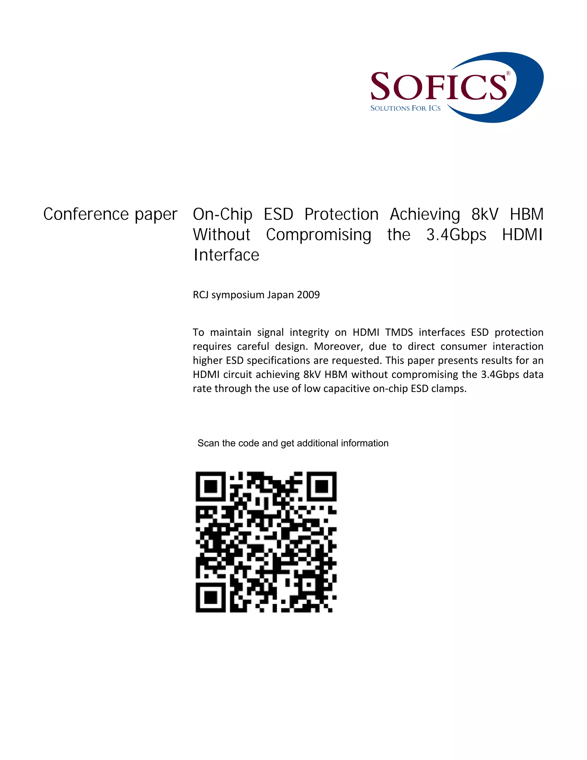
Conference paper On-Chip ESD Protection Achieving 8kV HBM
Without Compromising the 3.4Gbps HDMI
Interface
 
RCJ symposium Japan 2009 
 
To  maintain  signal  integrity  on  HDMI  TMDS  interfaces  ESD  protection 
requires  careful  design.  Moreover,  due  to  direct  consumer  interaction 
higher ESD specifications are requested. This paper presents results for an 
HDMI circuit achieving 8kV HBM without compromising the 3.4Gbps data 
rate through the use of low capacitive on‐chip ESD clamps. 
Scan the code and get additional information.
On-Chip ESD Protection Achieving 8kV HBM
Without Compromising the 3.4Gbps HDMI Interface
M. Roseeuw, J. Binnemans, B. Keppens and K. Verhaege
Sofics BVBA, Brugse Baan 188A, B-8470 Gistel, Belgium
This paper is co-copyrighted by Sofics and the RCJ symposium
Abstract – To maintain signal integrity on HDMI TMDS
interfaces ESD protection requires careful design. Moreover, due
to direct consumer interaction higher ESD specifications are
requested. This paper presents results for an HDMI circuit
achieving 8kV HBM without compromising the 3.4Gbps data
rate through the use of low capacitive on-chip ESD clamps.
I. INTRODUCTION
HDMI (High Definition Multimedia Interface) allows the
transmission of uncompressed digital audio and/or video data
between consumer applications. Nowadays, HDMI is already
widely implemented and is estimated to grow beyond one
billion devices by 2010 [1] covering all kinds of multimedia
applications. The HDMI standard requires high bandwidth
data transmission in order to achieve superior quality, which is
desirable for, e.g. HDTV. As can be seen from Fig. 1 [2] there
are three TMDS channels (Transition Minimized Differential
Signaling) each with a maximum data rate of 3.4 Gbps.
Fig. 1. Overview of HDMI channels [2]
One of the challenges is to maintain the signal integrity while
relying on reasonably priced cable assemblies and practical
cable lengths of several meters. For instance, parasitic
capacitance to ground and between twisted pair wires along
the channel must be reduced as much as possible as it will
deteriorate the signal integrity. In order to test for the signal
integrity, the HDMI specification defines a minimal eye
opening for the TMDS channels. It is therefore important to
carefully design the ESD (Electrostatic Discharge) protection
with low parasitic capacitance to ensure crisp picture quality.
Due to direct and typical careless consumer interaction ESD
requirement levels included into the HDMI compliance tests
are very severe (8kV IEC 61000-4-2 contact discharge [3])
translating into ESD protection with high current shunting
capabilities. This qualification test is believed to correlate with
user interaction like plugging possibly charged HDMI cables
during powered conditions. Such interaction causes overstress
on the board but should not damage the connected appliances.
OEM system builders have solved these ESD requirements
with board level, off-chip components in the past. However, in
an effort to save board area, reduce design time and reduce
board level parasitic elements IC manufacturers are now being
forced to include on-chip ESD protection with above standard
levels: e.g. 8kV HBM (Human Body Model) instead of 2kV
[4].
Through the continued technology scaling, the RF
characteristics of MOS transistors are constantly improving.
This makes it more attractive to implement structures
supporting high speed interfaces like HDMI. But this
technology scaling also implies a reduction of ESD design
margins. This is illustrated by Fig.2. The difference between
the failure voltage (‘Maximum voltage’) and the maximum
operating voltage (‘Vdd’) is the ESD design window. This is
the margin in which the ESD device is allowed to operate
without disturbing the regular circuit operation while
protecting the sensitive devices.
Fig. 2. Scaling ESD design window
The next section describes and compares two protection
strategies. Section III provides a detailed description of the on-
chip ESD protection approach and includes analysis results of
an HDMI application whereby both Tx (transmitter or source)
and Rx (Receiver or sink) circuits are protected against 8kV
HBM using low capacitive (less than 600fF) on-chip ESD
0 5 10 15 20 25
Node [nm]
V [V]
Maximum
voltageVdd
500
350
250
180
130
90
65
45
ESD design
window
clamps. Further, to achieve the maximum data rate the
capacitance and resistance of the Tx output drivers is limited
as much as possible through the use of extremely sensitive
fully silicided MOS devices. Such robust and low capacitive
on-chip protection provides much needed headroom for the
system builders.
The DDC (Data Display Channel) is an I²C (Inter IC
Communication) link [5] and is a low bit rate signal that can
tolerate a much higher parasitic capacitance. However the
maximum voltage can go beyond the 3.3 V level and a
specific 5 V tolerant ESD protection clamp is required. Such a
solution is described at the end of the paper.
II. OFF-CHIP AND ON-CHIP PROTECTION APPROACHES
There is a push in some industries to incorporate system
level ESD (IEC 61000-4-2) protection on the component level.
Especially for ICs that provide interfaces to the external world
like HDMI and USB. There are various reasons for this push.
From a system level view, less board space and reduced BOM
(Bill of Materials) results in cost reduction, reduced design
time and design cycles and leads to smaller appliances. The
design effort and area overhead for increasing the component
level ESD robustness to system level specification is not
excessive. On chip protection is also automatically adjusted to
the used process technology and will fit the ESD design
window.
Fig. 3. Circuit view of a typical off-chip low capacitive ESD protection device
At this moment, there is no standard way to apply IEC 61000-
4-2 to an individual component. One approach is to use an
IEC 62228 like approach [6][7]: the IC to be tested is soldered
to a circuit board that extends the IC pins to a connector used
in system. Further, circuitry can be added to be able to test the
IC in powered mode. By applying the IEC stress to the
connector pins, the IC can then be qualified. This approach
however is often too severe for the IC component. On the
actual system, the board will be more complex with various
discharge paths as signal lines are shared amongst multiple
components. Discrete and parasitic capacitors may store most
of the ESD charge and reduce the peak voltage and current
through the ICs. Trace inductances and resistances have
similar effects. Therefore this IEC 62228 is currently limited
to one specific application type: the automotive CAN-bus [6].
Attempts have been made to provide a more accurate
correlation between HBM and system level ESD [8-9].
However, establishing this correlation is not trivial. Again,
since this is a component level test, the actual system is not
taken into account.
To provide a compromise, the IC discussed in this paper is
designed for 8kV component level HBM. Since this is an IC
that directly interfaces with a connector, a higher HBM
performance level was chosen to increase the design margin
on the board level.
0
2
4
6
8
10
2 4 6 8 10 12 14 16
REF2 to REF1
IO1 to REF1
I [A]
V [V]
Fig. 4. TLP plot of the stress case from REF2 to REF1 (blue) and from IO1 to
REF1 (red)
An alternative is to use off chip IEC level ESD protection
devices. Fig.3. shows a typical low capacitive off-chip
protection device. Note that for some devices capacitance C1
is mandatory.
Fig.4. shows a TLP (Transmission Line Pulse) plot for two
stress cases measured on a stand-alone board level protection.
Note that the voltage runs up to over 14.4 V for the stress case
from IO1 to ref1. Moreover, the transient overshoot is reported
to be a factor of 10 higher for many board level components
[6]. If this voltage is applied at the IC IO’s it will fail. There
are however board level layout techniques to prevent this [10].
The use of an on-chip protection up to 8kV HBM increases the
design margins.
III. ON-CHIP PROTECTION APPROACH
The HDMI application circuit is fabricated on a 0.13 µm
technology. The IC has both TMDS inputs and outputs.
Shown in Fig.5. is a simplified example of a TMDS output
used in a HDMI transmitter. Transistor M1 and M2 are
switching transistors, transistor M3 acts as a current source.
Transistors M1 and M2 are fully silicided NMOS devices to
minimize resistivity and capacitive loading. M1 and M2 are
cascoded with M3, leading to a maximum tolerated voltage at
the Dout pin of 11V during ESD stress. To maximize this
voltage it is not possible to merge any of these transistor
elements. The ESD protection must shunt the current below
this voltage.
Fig. 5. Example of an TMDS output
Due to CML approach (Current Mode Logic) the ESD
protection of transistors M1 and M2 has to be overvoltage
tolerant. A diode from pad to Vdd is not allowed. The ESD
protection consists of a local clamp and a diode. This approach
is usually applied because it offers the lowest voltage across
the protected pin. The local clamp is a so-called GG-SCR
(NMOS triggered Silicon Controlled Rectifier), as shown in
Fig.6. This is a very fast triggered clamp [11]. The triggering
voltage of this system is 9.6 V, which is lower than the
maximal voltage allowed voltage at the output. The clamping
voltage of maximal 6.7 V allows a current shunting capability
at low voltages; as a consequence there is optimal power
dissipation per area during an ESD event.
Fig. 6. Implementation of the ESD protection
In order to obtain the desired specifications (8kV HBM), the
clamp perimeter needs to be enlarged from the standard value
of 60 µm (failure current of 2.45 A) to 160 µm (failure current
of 6.5A), leading to a total area consumption of 2830 µm² for
the ESD protection (local clamp and diode). The parasitic
junction capacitance is 587 fF. A TLP plot of the stand-alone
60 µm SCR clamp is depicted in Fig.7.
ESD protection is also necessary at the input pins. A typical
HDMI input consists of an input gate with a pull up resistor to
the power supply. The maximal allowed voltage at the input
pins is 13 V. In this case a dual diode ESD protection
approach is used. The core protection clamp consists of an
RCSCR (RC-triggered SCR) with 3 extra diodes at its anode
for improved latch up immunity. A circuit overview and TLP
plot of this clamp are shown in Fig.8, Fig.9 respectively.
0
0.5
1
1.5
2
2.5
0 2 4 6 8 10
10
-11
10
-9
10
-7
10
-5
10
-3
Local GGSCR
Leakage
I [A]
V [V]
Fig. 7. TLP plot of the GGSCR protection
Fig. 8. 3.3 V domain protection strategy
0
1
2
3
4
5
0 5 10 15
10
-11
10
-9
10
-7
10
-5
10
-3
RCSCR PC
Leakage
I [A]
V [V]
Fig. 9. TLP plot of the RCSCR protection
The chip circuitry operates in a 3.3 V domain. However the
studied HDMI application required some IO’s to be 5 V
tolerant. These 5V tolerant pins further decrease the ESD
design window. For these pins, the capacitive load is less
important, because the signal bandwidth is much lower and a
larger clamp size can be used.
A cascoded MOS configuration with specific ESD
enhancements is included in the circuit. The measurements of
this device are summarized by the TLP plot shown in Fig.10.
Fig. 10. TLP plot 5 V tolerant pins
The qualification of the protection in the complete HDMI
circuit was performed by an external test house. The HBM
level exceeds 8kV as targeted.
V. CONCLUSION
The HDMI interface is included in a broad range of
consumer applications for high quality multimedia content.
Sources estimate more than 1 billion HDMI capable devices
by 2010.
To enable superb image quality (1080p, 16 bit deep color) a
data rate of 3.4 Gbps is used for the video carrying TMDS
channels. Such data rate requires careful design of the
connector, board level components and IC IO structures in
order to maintain signal integrity. Moreover, due to direct
consumer interaction higher ESD specifications are typically
requested. OEM system builders have solved these ESD
requirements with board level, off-chip components in the
past. However, in an effort to save board area, reduce design
time and reduce board level parasitic IC manufacturers are
now being forced to include on-chip ESD protection with
above standard levels (e.g. 8kV HBM instead of 2kV).
This paper presented results for a HDMI circuit achieving 8kV
HBM without compromising the 3.4Gbps data rate through the
use of low capacitive on-chip ESD clamps, creating additional
head-room for the system builders. The HDMI application
example used both Tx (transmitter or source) and Rx
(Receiver or sink) circuits. To limit the capacitance and
resistance of the Tx output drivers extremely sensitive fully
silicided MOS devices were used.
NOTE
As is the case with many published ESD design solutions,
most of the techniques and protection solutions described in
this paper are covered under patents and cannot be copied
freely.
ACKNOWLEDGMENTS
The authors gratefully acknowledge their colleagues at
Sarnoff Europe and more specifically Bart Sorgeloos and Ilse
Backers.
REFERENCES
[1] HDMI website; http://www.hdmi.org
[2] Hitachi, Ltd.; Matsushita Electric Industrial Co., Ltd.; Philips Consumer
Electronics, International B.V.; Silicon Image, Inc. Sony Corporation;
Thomson Inc.; Toshiba Corporation, “High Definition Multimedia
Interface Specification Version 1.3a,” November 10, 2006
[3] IEC 61000-4-2; April 2004
[4] Ismini Scouras, “HDMI stars on small screens,” EE Times 10/29/2007
[5] Phillips Semiconductors, “The I²C-bus specification version 2.1,”
January 2000
[6] Robert A. Ashton, “Where Should We Be Putting Our ESD Resources,”
Keynote Taiwan ESD Conference, 2008
[7] Dening Wang, “Application of IEC 61000-4-2 in Component Level,”
ESD council, March 03, 2003
[8] W. Stadler, “From the ESD robustness of Products to the System ESD
Robustness,” EOS/ESD Symposium, 2004
[9] T. Smedes, J. van Zwol, G. de Raad, T. Brodbeck and H. wolf,
“Relations between system level ESD and (vf-)TLP,” EOS/ESD
Symposium 2006
[10] Infineon Technologies AG, “ESD Protection for Digital High-Speed
Interfaces using ESD5V3U1U,” Application Note No. 140, 2008
[11] Russ, C. et al., “GGSCRs: GGNMOS Triggered Silicon Controlled
Rectifiers for ESD Protection in Deep Sub-Micron CMOS Processes”,
EOS/ESD 2001
Sofics Proprietary – ©2011
About Sofics
Sofics  (www.sofics.com)  is  the  world  leader  in  on‐chip  ESD  protection.  Its 
patented  technology  is  proven  in  more  than  a  thousand  IC  designs  across  all 
major foundries and process nodes. IC companies of all sizes rely on Sofics for off‐
the‐shelf  or  custom‐crafted  solutions  to  protect  overvoltage  I/Os,  other  non‐
standard  I/Os,  and  high‐voltage  ICs,  including  those  that  require  system‐level 
protection on the chip. Sofics technology produces smaller I/Os than any generic 
ESD configuration. It also permits twice the IC performance in high‐frequency and 
high‐speed applications. Sofics ESD solutions and service begin where the foundry 
design manual ends. 
Our service and support
Our business models include 
• Single‐use, multi‐use or royalty bearing license for ESD clamps 
• Services to customize ESD protection 
o Enable unique requirements for Latch‐up, ESD, EOS 
o Layout, metallization and aspect ratio customization 
o Area, capacitance, leakage optimization 
• Transfer of individual clamps to another target technology 
• Develop custom ESD clamps for foundry or proprietary process 
• Debugging and correcting an existing IC or IO 
• ESD testing and analysis 
Notes
As  is  the  case  with  many  published  ESD  design  solutions,  the  techniques  and 
protection  solutions  described  in  this  data  sheet  are  protected  by  patents  and 
patents  pending  and  cannot  be  copied  freely.  PowerQubic,  TakeCharge,  and 
Sofics are trademarks of Sofics BVBA. 
Version
May 2011
  
  ESD SOLUTIONS AT YOUR FINGERTIPS 
Sofics BVBA 
Groendreef 31 
B‐9880 Aalter, Belgium 
(tel) +32‐9‐21‐68‐333 
(fax) +32‐9‐37‐46‐846 
bd@sofics.com 
RPR 0472.687.037 

On-Chip ESD Protection Achieving 8kV HBM Without Compromising the 3.4Gbps HDMI Interface

  • 1.
    Conference paper On-ChipESD Protection Achieving 8kV HBM Without Compromising the 3.4Gbps HDMI Interface   RCJ symposium Japan 2009    To  maintain  signal  integrity  on  HDMI  TMDS  interfaces  ESD  protection  requires  careful  design.  Moreover,  due  to  direct  consumer  interaction  higher ESD specifications are requested. This paper presents results for an  HDMI circuit achieving 8kV HBM without compromising the 3.4Gbps data  rate through the use of low capacitive on‐chip ESD clamps.  Scan the code and get additional information.
  • 2.
    On-Chip ESD ProtectionAchieving 8kV HBM Without Compromising the 3.4Gbps HDMI Interface M. Roseeuw, J. Binnemans, B. Keppens and K. Verhaege Sofics BVBA, Brugse Baan 188A, B-8470 Gistel, Belgium This paper is co-copyrighted by Sofics and the RCJ symposium Abstract – To maintain signal integrity on HDMI TMDS interfaces ESD protection requires careful design. Moreover, due to direct consumer interaction higher ESD specifications are requested. This paper presents results for an HDMI circuit achieving 8kV HBM without compromising the 3.4Gbps data rate through the use of low capacitive on-chip ESD clamps. I. INTRODUCTION HDMI (High Definition Multimedia Interface) allows the transmission of uncompressed digital audio and/or video data between consumer applications. Nowadays, HDMI is already widely implemented and is estimated to grow beyond one billion devices by 2010 [1] covering all kinds of multimedia applications. The HDMI standard requires high bandwidth data transmission in order to achieve superior quality, which is desirable for, e.g. HDTV. As can be seen from Fig. 1 [2] there are three TMDS channels (Transition Minimized Differential Signaling) each with a maximum data rate of 3.4 Gbps. Fig. 1. Overview of HDMI channels [2] One of the challenges is to maintain the signal integrity while relying on reasonably priced cable assemblies and practical cable lengths of several meters. For instance, parasitic capacitance to ground and between twisted pair wires along the channel must be reduced as much as possible as it will deteriorate the signal integrity. In order to test for the signal integrity, the HDMI specification defines a minimal eye opening for the TMDS channels. It is therefore important to carefully design the ESD (Electrostatic Discharge) protection with low parasitic capacitance to ensure crisp picture quality. Due to direct and typical careless consumer interaction ESD requirement levels included into the HDMI compliance tests are very severe (8kV IEC 61000-4-2 contact discharge [3]) translating into ESD protection with high current shunting capabilities. This qualification test is believed to correlate with user interaction like plugging possibly charged HDMI cables during powered conditions. Such interaction causes overstress on the board but should not damage the connected appliances. OEM system builders have solved these ESD requirements with board level, off-chip components in the past. However, in an effort to save board area, reduce design time and reduce board level parasitic elements IC manufacturers are now being forced to include on-chip ESD protection with above standard levels: e.g. 8kV HBM (Human Body Model) instead of 2kV [4]. Through the continued technology scaling, the RF characteristics of MOS transistors are constantly improving. This makes it more attractive to implement structures supporting high speed interfaces like HDMI. But this technology scaling also implies a reduction of ESD design margins. This is illustrated by Fig.2. The difference between the failure voltage (‘Maximum voltage’) and the maximum operating voltage (‘Vdd’) is the ESD design window. This is the margin in which the ESD device is allowed to operate without disturbing the regular circuit operation while protecting the sensitive devices. Fig. 2. Scaling ESD design window The next section describes and compares two protection strategies. Section III provides a detailed description of the on- chip ESD protection approach and includes analysis results of an HDMI application whereby both Tx (transmitter or source) and Rx (Receiver or sink) circuits are protected against 8kV HBM using low capacitive (less than 600fF) on-chip ESD 0 5 10 15 20 25 Node [nm] V [V] Maximum voltageVdd 500 350 250 180 130 90 65 45 ESD design window
  • 3.
    clamps. Further, toachieve the maximum data rate the capacitance and resistance of the Tx output drivers is limited as much as possible through the use of extremely sensitive fully silicided MOS devices. Such robust and low capacitive on-chip protection provides much needed headroom for the system builders. The DDC (Data Display Channel) is an I²C (Inter IC Communication) link [5] and is a low bit rate signal that can tolerate a much higher parasitic capacitance. However the maximum voltage can go beyond the 3.3 V level and a specific 5 V tolerant ESD protection clamp is required. Such a solution is described at the end of the paper. II. OFF-CHIP AND ON-CHIP PROTECTION APPROACHES There is a push in some industries to incorporate system level ESD (IEC 61000-4-2) protection on the component level. Especially for ICs that provide interfaces to the external world like HDMI and USB. There are various reasons for this push. From a system level view, less board space and reduced BOM (Bill of Materials) results in cost reduction, reduced design time and design cycles and leads to smaller appliances. The design effort and area overhead for increasing the component level ESD robustness to system level specification is not excessive. On chip protection is also automatically adjusted to the used process technology and will fit the ESD design window. Fig. 3. Circuit view of a typical off-chip low capacitive ESD protection device At this moment, there is no standard way to apply IEC 61000- 4-2 to an individual component. One approach is to use an IEC 62228 like approach [6][7]: the IC to be tested is soldered to a circuit board that extends the IC pins to a connector used in system. Further, circuitry can be added to be able to test the IC in powered mode. By applying the IEC stress to the connector pins, the IC can then be qualified. This approach however is often too severe for the IC component. On the actual system, the board will be more complex with various discharge paths as signal lines are shared amongst multiple components. Discrete and parasitic capacitors may store most of the ESD charge and reduce the peak voltage and current through the ICs. Trace inductances and resistances have similar effects. Therefore this IEC 62228 is currently limited to one specific application type: the automotive CAN-bus [6]. Attempts have been made to provide a more accurate correlation between HBM and system level ESD [8-9]. However, establishing this correlation is not trivial. Again, since this is a component level test, the actual system is not taken into account. To provide a compromise, the IC discussed in this paper is designed for 8kV component level HBM. Since this is an IC that directly interfaces with a connector, a higher HBM performance level was chosen to increase the design margin on the board level. 0 2 4 6 8 10 2 4 6 8 10 12 14 16 REF2 to REF1 IO1 to REF1 I [A] V [V] Fig. 4. TLP plot of the stress case from REF2 to REF1 (blue) and from IO1 to REF1 (red) An alternative is to use off chip IEC level ESD protection devices. Fig.3. shows a typical low capacitive off-chip protection device. Note that for some devices capacitance C1 is mandatory. Fig.4. shows a TLP (Transmission Line Pulse) plot for two stress cases measured on a stand-alone board level protection. Note that the voltage runs up to over 14.4 V for the stress case from IO1 to ref1. Moreover, the transient overshoot is reported to be a factor of 10 higher for many board level components [6]. If this voltage is applied at the IC IO’s it will fail. There are however board level layout techniques to prevent this [10]. The use of an on-chip protection up to 8kV HBM increases the design margins. III. ON-CHIP PROTECTION APPROACH The HDMI application circuit is fabricated on a 0.13 µm technology. The IC has both TMDS inputs and outputs. Shown in Fig.5. is a simplified example of a TMDS output used in a HDMI transmitter. Transistor M1 and M2 are switching transistors, transistor M3 acts as a current source. Transistors M1 and M2 are fully silicided NMOS devices to minimize resistivity and capacitive loading. M1 and M2 are cascoded with M3, leading to a maximum tolerated voltage at
  • 4.
    the Dout pinof 11V during ESD stress. To maximize this voltage it is not possible to merge any of these transistor elements. The ESD protection must shunt the current below this voltage. Fig. 5. Example of an TMDS output Due to CML approach (Current Mode Logic) the ESD protection of transistors M1 and M2 has to be overvoltage tolerant. A diode from pad to Vdd is not allowed. The ESD protection consists of a local clamp and a diode. This approach is usually applied because it offers the lowest voltage across the protected pin. The local clamp is a so-called GG-SCR (NMOS triggered Silicon Controlled Rectifier), as shown in Fig.6. This is a very fast triggered clamp [11]. The triggering voltage of this system is 9.6 V, which is lower than the maximal voltage allowed voltage at the output. The clamping voltage of maximal 6.7 V allows a current shunting capability at low voltages; as a consequence there is optimal power dissipation per area during an ESD event. Fig. 6. Implementation of the ESD protection In order to obtain the desired specifications (8kV HBM), the clamp perimeter needs to be enlarged from the standard value of 60 µm (failure current of 2.45 A) to 160 µm (failure current of 6.5A), leading to a total area consumption of 2830 µm² for the ESD protection (local clamp and diode). The parasitic junction capacitance is 587 fF. A TLP plot of the stand-alone 60 µm SCR clamp is depicted in Fig.7. ESD protection is also necessary at the input pins. A typical HDMI input consists of an input gate with a pull up resistor to the power supply. The maximal allowed voltage at the input pins is 13 V. In this case a dual diode ESD protection approach is used. The core protection clamp consists of an RCSCR (RC-triggered SCR) with 3 extra diodes at its anode for improved latch up immunity. A circuit overview and TLP plot of this clamp are shown in Fig.8, Fig.9 respectively. 0 0.5 1 1.5 2 2.5 0 2 4 6 8 10 10 -11 10 -9 10 -7 10 -5 10 -3 Local GGSCR Leakage I [A] V [V] Fig. 7. TLP plot of the GGSCR protection Fig. 8. 3.3 V domain protection strategy
  • 5.
    0 1 2 3 4 5 0 5 1015 10 -11 10 -9 10 -7 10 -5 10 -3 RCSCR PC Leakage I [A] V [V] Fig. 9. TLP plot of the RCSCR protection The chip circuitry operates in a 3.3 V domain. However the studied HDMI application required some IO’s to be 5 V tolerant. These 5V tolerant pins further decrease the ESD design window. For these pins, the capacitive load is less important, because the signal bandwidth is much lower and a larger clamp size can be used. A cascoded MOS configuration with specific ESD enhancements is included in the circuit. The measurements of this device are summarized by the TLP plot shown in Fig.10. Fig. 10. TLP plot 5 V tolerant pins The qualification of the protection in the complete HDMI circuit was performed by an external test house. The HBM level exceeds 8kV as targeted. V. CONCLUSION The HDMI interface is included in a broad range of consumer applications for high quality multimedia content. Sources estimate more than 1 billion HDMI capable devices by 2010. To enable superb image quality (1080p, 16 bit deep color) a data rate of 3.4 Gbps is used for the video carrying TMDS channels. Such data rate requires careful design of the connector, board level components and IC IO structures in order to maintain signal integrity. Moreover, due to direct consumer interaction higher ESD specifications are typically requested. OEM system builders have solved these ESD requirements with board level, off-chip components in the past. However, in an effort to save board area, reduce design time and reduce board level parasitic IC manufacturers are now being forced to include on-chip ESD protection with above standard levels (e.g. 8kV HBM instead of 2kV). This paper presented results for a HDMI circuit achieving 8kV HBM without compromising the 3.4Gbps data rate through the use of low capacitive on-chip ESD clamps, creating additional head-room for the system builders. The HDMI application example used both Tx (transmitter or source) and Rx (Receiver or sink) circuits. To limit the capacitance and resistance of the Tx output drivers extremely sensitive fully silicided MOS devices were used. NOTE As is the case with many published ESD design solutions, most of the techniques and protection solutions described in this paper are covered under patents and cannot be copied freely. ACKNOWLEDGMENTS The authors gratefully acknowledge their colleagues at Sarnoff Europe and more specifically Bart Sorgeloos and Ilse Backers. REFERENCES [1] HDMI website; http://www.hdmi.org [2] Hitachi, Ltd.; Matsushita Electric Industrial Co., Ltd.; Philips Consumer Electronics, International B.V.; Silicon Image, Inc. Sony Corporation; Thomson Inc.; Toshiba Corporation, “High Definition Multimedia Interface Specification Version 1.3a,” November 10, 2006 [3] IEC 61000-4-2; April 2004 [4] Ismini Scouras, “HDMI stars on small screens,” EE Times 10/29/2007 [5] Phillips Semiconductors, “The I²C-bus specification version 2.1,” January 2000 [6] Robert A. Ashton, “Where Should We Be Putting Our ESD Resources,” Keynote Taiwan ESD Conference, 2008 [7] Dening Wang, “Application of IEC 61000-4-2 in Component Level,” ESD council, March 03, 2003 [8] W. Stadler, “From the ESD robustness of Products to the System ESD Robustness,” EOS/ESD Symposium, 2004 [9] T. Smedes, J. van Zwol, G. de Raad, T. Brodbeck and H. wolf, “Relations between system level ESD and (vf-)TLP,” EOS/ESD Symposium 2006 [10] Infineon Technologies AG, “ESD Protection for Digital High-Speed Interfaces using ESD5V3U1U,” Application Note No. 140, 2008 [11] Russ, C. et al., “GGSCRs: GGNMOS Triggered Silicon Controlled Rectifiers for ESD Protection in Deep Sub-Micron CMOS Processes”, EOS/ESD 2001
  • 6.
    Sofics Proprietary –©2011 About Sofics Sofics  (www.sofics.com)  is  the  world  leader  in  on‐chip  ESD  protection.  Its  patented  technology  is  proven  in  more  than  a  thousand  IC  designs  across  all  major foundries and process nodes. IC companies of all sizes rely on Sofics for off‐ the‐shelf  or  custom‐crafted  solutions  to  protect  overvoltage  I/Os,  other  non‐ standard  I/Os,  and  high‐voltage  ICs,  including  those  that  require  system‐level  protection on the chip. Sofics technology produces smaller I/Os than any generic  ESD configuration. It also permits twice the IC performance in high‐frequency and  high‐speed applications. Sofics ESD solutions and service begin where the foundry  design manual ends.  Our service and support Our business models include  • Single‐use, multi‐use or royalty bearing license for ESD clamps  • Services to customize ESD protection  o Enable unique requirements for Latch‐up, ESD, EOS  o Layout, metallization and aspect ratio customization  o Area, capacitance, leakage optimization  • Transfer of individual clamps to another target technology  • Develop custom ESD clamps for foundry or proprietary process  • Debugging and correcting an existing IC or IO  • ESD testing and analysis  Notes As  is  the  case  with  many  published  ESD  design  solutions,  the  techniques  and  protection  solutions  described  in  this  data  sheet  are  protected  by  patents  and  patents  pending  and  cannot  be  copied  freely.  PowerQubic,  TakeCharge,  and  Sofics are trademarks of Sofics BVBA.  Version May 2011      ESD SOLUTIONS AT YOUR FINGERTIPS  Sofics BVBA  Groendreef 31  B‐9880 Aalter, Belgium  (tel) +32‐9‐21‐68‐333  (fax) +32‐9‐37‐46‐846  bd@sofics.com  RPR 0472.687.037